

Page 1
DATA BULLETIN
CMX644A
2000 MX-COM, Inc. www.mxcom.com tel: 800 638 5577 336 744 5050 fax: 336 744 5054 Doc. # 20480197.006
4800 Bethania Station Road,Winston-Salem,NC 27105-1201 USA All trademarks and service marks are held by their respective companies.
Bell 212A and V.22 Modem
with Call Progress and DTMF
PRELIMINARY INFORMATION
Features
• Bell 212A and V.22 Compatible Modem
• 1200bps Full Duplex Operation (2 or 4 Wire)
• UART for Start/Parity/Stop bit processing
• Non-UART Operating Mode
• Software Adjustable Tx and Rx Levels
• Programmable Group Delay Equalizer
• Answer/Originate Tone Generator/Detector
• Call Progress Tone Detection
• Integrated DTMF Encoder
• Line Reversal and Ring Detector
• Hook Switch Relay Driver
• Flexible Xtal/Master Clock Selection
• Simple Serial Control Interface
• Zero-Power Standby Mode
• 3.0V to 5.0V Operation
Applications
• Telephone Telemetry Systems
• Remote Utility Meter Reading
• Security Systems
• Payphones
• Cable-TV Set-Top Boxes
• Industrial Control Systems
• Electronic Cash Terminals
• Vending Machines
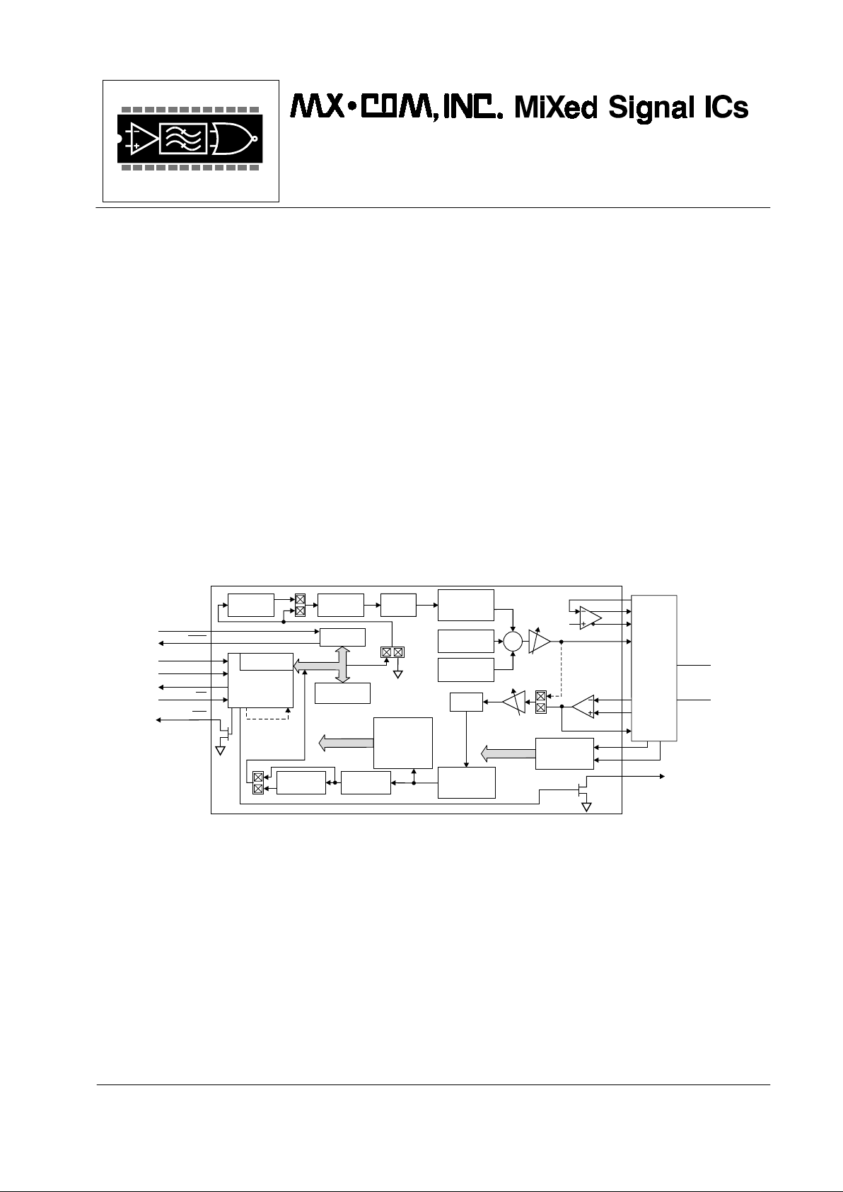
Unscrambler
PSK
Modulator
Tx
Filter
Tone
Generator 1
Local
Analog
Loopback
Control &
Data Registers
Carrier,
Call Progress,
AnswerTone
Detectors
Registers
Rx
Filter
PSK
Demodulator
Ring & Line
Reversal
Detect
Tx
Programmable
Equalizer
COMMAND
Oscillator
Clocks
Scrambler
XTAL/CLK
CS
SERIAL CLK
PASSIVE
HYBRID
NETWORK
2 or 4
Wire Line
Rx
Programmable
Equalizer
TX+
V
BIAS
RX-
RXAMPOUT
RD
RT
RL YDRV
XTAL
RX+
Tone
Generator 2
Rx Data
Serial
Interface
Local Digital
Loopback
Tx Data
REPL Y
Registers
IRQ
TX
TXIN-
TX-
UART
The CMX644A Bell 212A / V.22 modem provides full duplex 1200bps data signaling suitable for telephonebased information and telemetry systems where low power operation is desired. Bell 212A / V.22 signaling
delivers fast-call set-up times and robust, error resistant, transmission in 2- or 4-wire line circuits. A rich set of
important additional functions enhances end product value while reducing size. These include: integrated
DTMF encoder for dial out functions, single tone encoder for ‘melody’ generation, answer tone
generator/detector, line reversal and ring detector for ‘waking’ up a sleeping µC, adjustable Tx and Rx gain,
and a low impedance pull down output for hook relay control. The addition of the answer tone
generator/detector and call progress tone detector makes the set-up of a telephone call much easier for the
host µC to accomplish.
Very low power telemetry and data collection applications are supported by the CMX644A’s ‘Zero Power’
standby mode in which the device will detect telephone line ringing voltage or line voltage reversal events.
The CMX644A is pin compatible with the CMX624 Bell 202 / V.23 modem, operates with a supply voltage
between 3.0V and 5.5V and is available in the following packages: 24-pin SSOP (CMX644AD5), 24-pin SOIC
(CMX644AD2), and 24-pin PDIP (CMX644AP4).
Page 2

Bell 212A / V.22 Modem with Call Progress and DTMF 2 CMX644A Preliminary Information
2000 MX-COM, Inc. www.mxcom.com tel: 800 638 5577 336 744 5050 fax: 336 744 5054 Doc. # 20480197.006
4800 Bethania Station Road, Winston-Salem, NC 27105-1201 USA All trademarks and service marks are held by their respective companies.
CONTENTS
Section Page
1 Block Diagram ............................................................................................................... 3
2 Signal List ...................................................................................................................... 4
3 External Components.................................................................................................... 6
4 General Description....................................................................................................... 7
4.1 ‘C-BUS’ Serial Interface .......................................................................................................7
4.2 UART....................................................................................................................................8
4.3 Software Description............................................................................................................9
4.3.1 Write-only ‘C-BUS’ Registers.................................................................................................9
4.3.2 Write-only Register Descriptions............................................................................................ 9
4.3.3 Read Only ‘C-BUS’ Registers .............................................................................................. 16
5 Application Notes........................................................................................................ 20
5.1 Line Interface......................................................................................................................20
5.1.1 4-Wire Line Interface............................................................................................................ 20
5.1.2 2-Wire Line Interface............................................................................................................ 21
5.2 Ring Detector Interface ......................................................................................................22
5.3 Software Protocol for Transmitting PSK Data Bytes..........................................................23
5.4 Software Protocol for Receiving PSK Data Bytes..............................................................23
5.5 Handling Underflow and Overflow Conditions....................................................................24
6 Performance Specification ......................................................................................... 26
6.1 Electrical Performance.......................................................................................................26
6.1.1 Absolute Maximum Ratings ................................................................................................. 26
6.1.2 Operating Limits................................................................................................................... 26
6.1.3 Operating Characteristics .................................................................................................... 27
6.1.4 Timing .................................................................................................................................. 29
6.2 Packaging...........................................................................................................................31
MX-COM, Inc. reserves the right to change specifications at any time and without notice.
Page 3
Bell 212A / V.22 Modem with Call Progress and DTMF 3 CMX644A Preliminary Information
2000 MX-COM, Inc. www.mxcom.com tel: 800 638 5577 336 744 5050 fax: 336 744 5054 Doc. # 20480197.006
4800 Bethania Station Road, Winston-Salem, NC 27105-1201 USA All trademarks and service marks are held by their respective companies.
1 Block Diagram
Figure 1: Block Diagram
Page 4
Bell 212A / V.22 Modem with Call Progress and DTMF 4 CMX644A Preliminary Information
2000 MX-COM, Inc. www.mxcom.com tel: 800 638 5577 336 744 5050 fax: 336 744 5054 Doc. # 20480197.006
4800 Bethania Station Road, Winston-Salem, NC 27105-1201 USA All trademarks and service marks are held by their respective companies.
2 Signal List
CMX644A
D2/D5/P4
Signal
Pin No. Name Type
Description
1
XTAL
output The inverted output of the on-chip oscillator.
2 XTAL/CLOCK input
The input to the on-chip oscillator, for external Xtal circuit
or clock.
3 SERIAL CLOCK input
The ‘C-BUS’ serial clock input. This clock, produced by
the µController, is used for the transfer timing of
commands to and from the device.
4 COMMAND DATA input
The ‘C-BUS’ serial data input from the µController. Data
is loaded into this device in 8-bit bytes, MSB (B7) first,
and LSB (B0) last, synchronized to the SERIAL CLOCK.
5 REPLY DATA tri-state
The ‘C-BUS’ serial data output to the µController. The
transmission of REPLY DATA bytes is synchronized to
the SERIAL CLOCK under control of the
CS
input. This
3-state output is held at high impedance when not
sending data to the µController.
6
CS
input
Chip Select. The ‘C-BUS’ data loading control function:
this input is provided by the µController. Data transfer
sequences are initiated, completed or aborted by the
CS
signal.
7
IRQ
output
This output indicates an interrupt condition to the
µController by going to a logic ‘0’. This is a ‘wire-ORable’
output, enabling the connection of up to 8 peripherals to 1
interrupt port on the µController. This pin has a low
impedance pull-down to logic ‘0’ when active and a high
impedance when inactive. An external pull-up resistor is
required.
8 TX output The output of the transmit gain control.
9 TX+ output The output of the line driver amplifier.
10 TXIN- input The inverting input to the line driver amplifier.
11 TX- output
The inverted output of the line driving amplifier. Pins TX+
and TX- provide symmetrical outputs for use with a
balanced load to give sufficient Tx line signal levels even
at low V
DD
.
12
V
SS
power The negative supply rail (ground).
13
V
BIAS
output
A bias line for the internally circuitry, held at V
DD
/2. This
pin must be decoupled by a capacitor mounted close to
the device pins.
14 RLYDRV output An open-drain output for controlling a relay.
15 RX+ input The non-inverting input of the receive op-amp.
16 RX- input The inverting input of the receive op-amp.
17 RXAMPOUT output The output of the receive op-amp.
18 RT bi-directional
Open-drain output and Schmitt trigger input forming part
of the Ring or Line Polarity Reversal detector. An
external resistor to V
DD
and a capacitor to VSSshould be
connected to RT to filter and extend the RD input signal.
19 RD Input to the Ring or Line Polarity Reversal Detector.
20, 21, 22 - N/C No connections should be made to these pins.
Page 5

Bell 212A / V.22 Modem with Call Progress and DTMF 5 CMX644A Preliminary Information
2000 MX-COM, Inc. www.mxcom.com tel: 800 638 5577 336 744 5050 fax: 336 744 5054 Doc. # 20480197.006
4800 Bethania Station Road, Winston-Salem, NC 27105-1201 USA All trademarks and service marks are held by their respective companies.
CMX644A
D2/D5/P4
Signal
Pin No. Name Type
Description
23 A/D CAP output
The reference voltage for the internal A to D of the
receiver. This pin must be decoupled by a capacitor
mounted close to the device pins.
24
V
DD
power
The positive supply rail. Levels and thresholds within the
device are proportional to this voltage. Should be
decoupled to V
SS
by a capacitor mounted close to the
device pins.
This device is capable of detecting and decoding small amplitude signals. It is recommended that the printed
circuit board be laid out with a ground plane in the CMX644A area to provide a low impedance connection
between the V
SS
pin and the VDDand V
BIAS
decoupling capacitors. The receive path should be protected as
much as possible from extraneous signals.
Table 1: Signal Lists
Page 6
Bell 212A / V.22 Modem with Call Progress and DTMF 6 CMX644A Preliminary Information
2000 MX-COM, Inc. www.mxcom.com tel: 800 638 5577 336 744 5050 fax: 336 744 5054 Doc. # 20480197.006
4800 Bethania Station Road, Winston-Salem, NC 27105-1201 USA All trademarks and service marks are held by their respective companies.
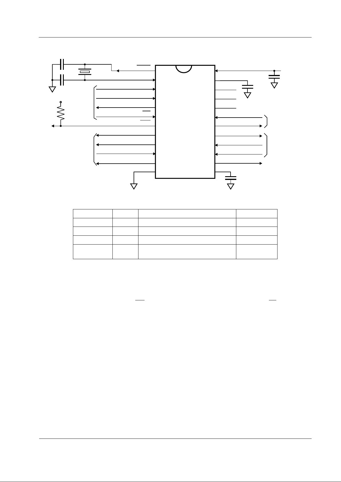
3 External Components
1
C1
C2
C5
C4
R1
X1
XTAL
XTAL/CLOCK
C-BUS
to/from
µC
Tx Line
Interface.
See 5.1
Rx Line
Interface.
See 5.1
To/from R in g
Detector.
See 5.2
SERIAL CLOCK
COMMAND DATA
REPLY D ATA
CS
IRQ
TX
RX+
RLYDRV
Relay Drive
RX-
RXAMPOUT
RT
RD
V
DD
V
DD
TXIN-
TX+
TXV
SS
2
3
4
CMX644A
D5/D2/P4
5
6
7
8
9
10
11
12
13
14
15
16
17
18
19
20
21
22
23
24
V
BIAS
N/C
N/C
A/D CAP
N/C
C3
Figure 2: Recommended External Components
R1 Note 1
100kΩ±1%
C1, C2 18pF
±20%
C3, C4,
0.1µF ±20%
C5
1µF ±20%
X1 3.6864MHz, 7.372800MHz or
11.0592MHz
Tolerances for Resistors and Capacitors are as indicated unless otherwise stated.
Table 2: Recommended External Components for Typical Application
Recommended External Component Notes on Xtal Osc and Clock Dividers
1. R1 should be selected so that the
IRQ
pin has returned to its normal (high) state before
CS
pin goes
high.
2. Frequency and timing accuracy of the CMX644A is determined by the clock present at the XTAL/CLOCK
pin. This may be generated by the on-chip oscillator inverter using the external components C1, C2 and
X1 of Figure 2, or may be supplied from an external source to the XTAL/CLOCK input. If the clock is
supplied from an external source, C1, C2 and X1 should not be fitted.
3. The on-chip oscillator is turned off in the 'Zero-Power' mode.
4. If the clock is provided by an external source that is not always running, then the 'Zero-Power' mode must
be set when the clock is not available. Failure to observe this rule may cause a rise in the supply current
drawn by CMX644A.
5. For best results, a crystal oscillator design should drive the clock inverter input with signal levels of at
least 40% of V
DD
, peak to peak. Tuning fork crystals generally cannot meet this requirement. To obtain
crystal oscillator design assistance, please consult your crystal manufacturer.
Page 7
Bell 212A / V.22 Modem with Call Progress and DTMF 7 CMX644A Preliminary Information
2000 MX-COM, Inc. www.mxcom.com tel: 800 638 5577 336 744 5050 fax: 336 744 5054 Doc. # 20480197.006
4800 Bethania Station Road, Winston-Salem, NC 27105-1201 USA All trademarks and service marks are held by their respective companies.
4 General Description
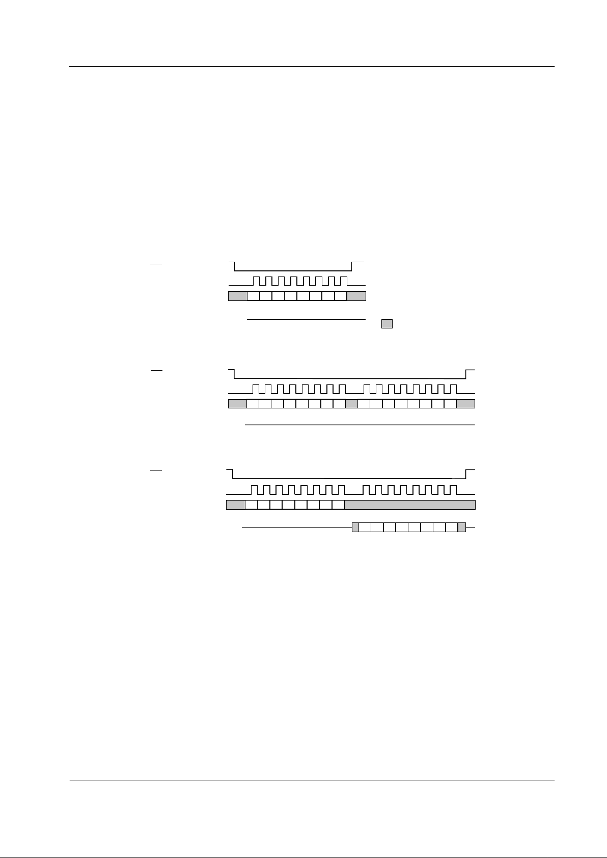
4.1 ‘C-BUS’ Serial Interface
This block provides for the transfer of data and control or status information between the CMX644A’s internal
registers and the µC over the ‘C-BUS’ serial bus. Each 'C-BUS' transaction consists of a single Register
Address byte sent from the µC, as illustrated in Figure 3, which may be followed by either of:
1. A single data byte sent from the µC to be written into one of the CMX644A’s Write Only Registers, as
illustrated in Figure 4.
2. A single byte of data read out from one of the CMX644A’s Read Only Registers, as illustrated in Figure 5.
Data sent from the µC on the COMMAND DATA line is clocked into the CMX644A on the rising edge of the
SERIAL CLOCK input. REPLY DATA sent from the CMX644A to the µC is valid when the SERIAL CLOCK is
high. The interface is compatible with the most common µC serial interfaces such as SCI, SPI and Microwire,
and may be easily implemented with general purpose µC I/O pins controlled by a simple software routine.
See Figure 15 for detailed ‘C-BUS’ timing requirements.
CS
SERIAL CLOCK
COMMAND DATA
Address (01 Hex = Reset)
= Level not important
Hi-Z
REPLY DATA
7
654
321
0
Figure 3: C-BUS Transactions (Single byte from µµµµC)
CS
SERIAL CLOCK
COMMAND DATA
Address
Hi-Z
Data to CMX644A
REPLY DATA
7
654
321
0
7
654
321
0
Figure 4: C-BUS Transactions (One Address and one Data byte from µµµµC)
CS
SERIAL CLOCK
Hi-Z
Address
Data from CM X 6 4 4 A
COMMAND DATA
REPLY DATA
7
654
321
0
7
654
321
0
Figure 5: C-BUS Transactions (One Address byte from µµµµC and one Reply byte from CMX644A)
Page 8
Bell 212A / V.22 Modem with Call Progress and DTMF 8 CMX644A Preliminary Information
2000 MX-COM, Inc. www.mxcom.com tel: 800 638 5577 336 744 5050 fax: 336 744 5054 Doc. # 20480197.006
4800 Bethania Station Road, Winston-Salem, NC 27105-1201 USA All trademarks and service marks are held by their respective companies.
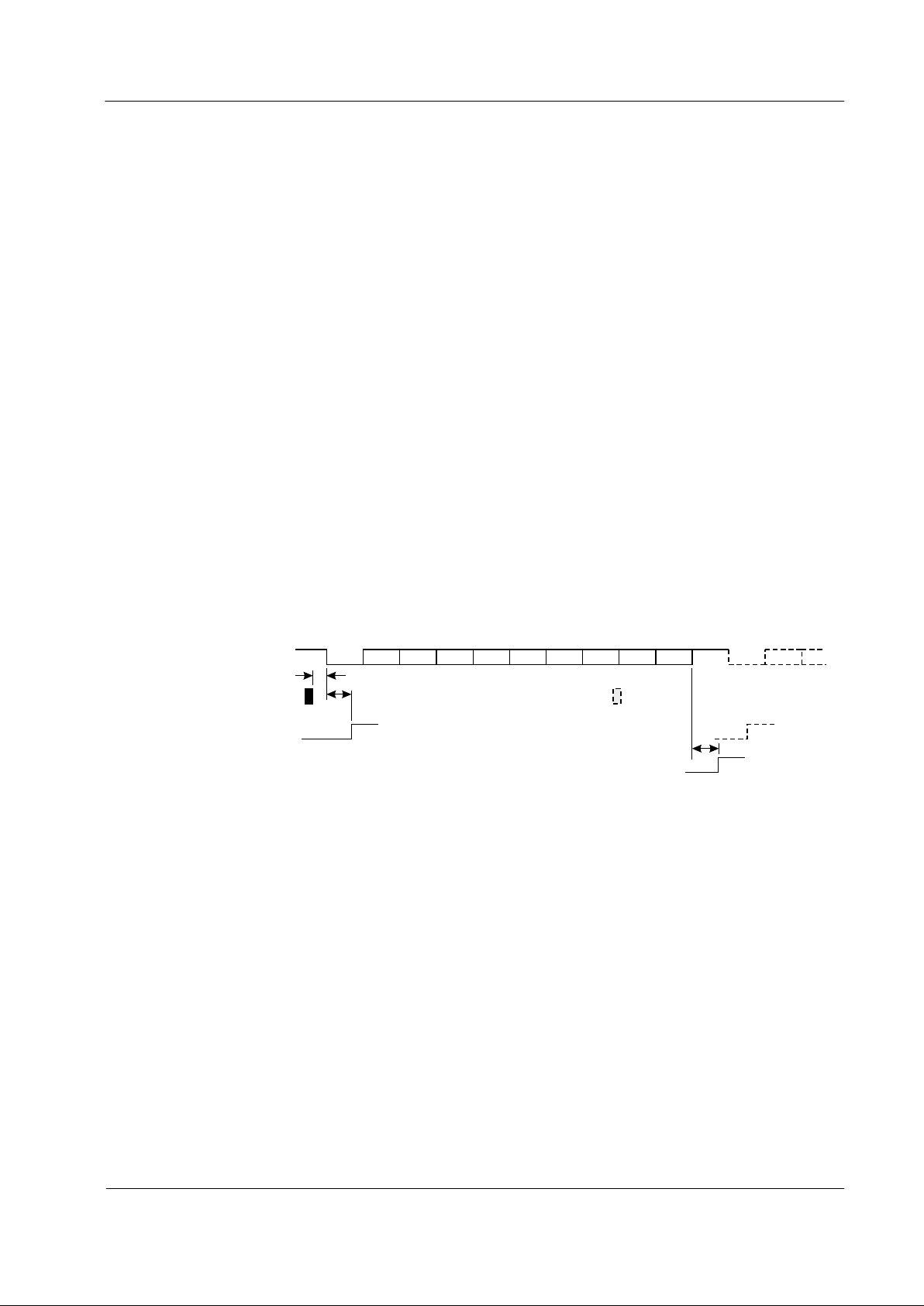
4.2 UART
This block connects the µC, via the ‘C-BUS’ interface, to the received data from the PSK Demodulator and to
the transmit data input to the PSK Modulator.
As part of the UART function, this block can be programmed to convert data that is to be transmitted from
7 or 8-bit bytes to asynchronous data characters, adding Start and Stop bits, and - optionally - a parity bit to
the data before passing it to the PSK Modulator. In the receive direction the UART can extract data bits from
asynchronous characters coming from the PSK Demodulator, stripping off the Start and Stop bits, and
performing an optional Parity check on the received data, before passing the result, via the ‘C-BUS’, to the
µC. Bits 0-5 of the UART MODE Register control the number of Stop and Data bits and the Parity options for
both receive and transmit directions.
Data to be transmitted should be loaded by the µC into the TX DATA BYTE Register when the Tx Data Ready
bit (bit 1) of the FLAGS Register goes high. It will then be treated by the Tx UART block in one of two ways,
depending on the setting of bit 5 of the UART MODE Register:
1. If bit 5 of the UART MODE Register is ‘0’ (‘Sync’ mode) then the 8 bits from the TX DATA BYTE Register
will be transmitted sequentially LSB (D0) first.
2. If bit 5 of the UART MODE Register is ‘1’ (‘Async’ mode) then the 7 or 8 bits will be transmitted as
asynchronous data characters according to the following format:
One Start bit (Space).
7 or 8 Data bits from the TX DATA BYTE Register (D0-D6 or D0-D7) as determined by bit 0 of the
UART MODE Register. LSB (D0) transmitted first.
Optional Parity bit (even or odd parity) as determined by bits 1 and 2 of the UART MODE Register.
Zero, One or Two Stop bits (Mark) as determined by bits 3 and 4 of the UART MODE Register.
In both cases data will only be transmitted if bit 6 of the TX PSK MODE Register is set to ‘1’.
Failure to load the TX DATA BYTE Register with a new value when required will result in bit 2 (TX DATA
UNDERFLOW) of the FLAGS Register being set to ‘1’ and a continuous Mark (‘1’) signal will then be
transmitted until a new value is loaded into TX DATA BYTE Register.
TX DATA R egister loaded:
Tx DATA PSK signal:
t
DEL
t
LOAD
t
UFL
TX DATA READY flag bit:
TX DATA UNDERFLO W flag bit:
D0 D0
Start Start
P'ty
Stop
D1 D2
D3
D4
D5 D6
D7
Figure 6: Transmit UART Function (Async)
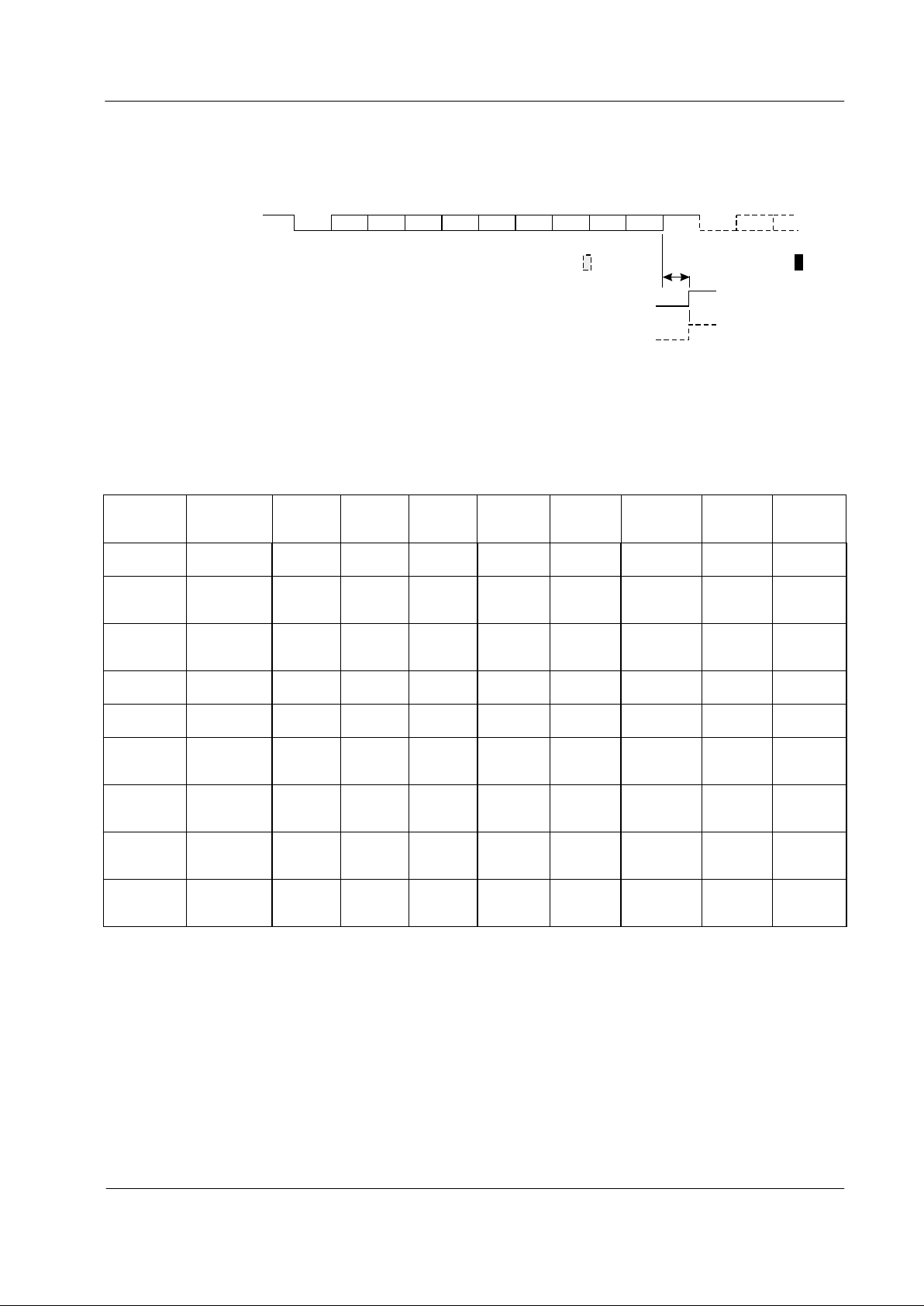
Received data from the PSK Demodulator goes into the receive part of the UART block, where it is handled in
one of two ways depending on the setting of bit 5 of the UART MODE Register:
1. If bit 5 of the UART MODE Register is ‘0’ (‘Sync’ mode) then the receive part of the UART block will
simply take 8 consecutive bits from the Demodulator and transfer them to the RX DATA BYTE Register
(the first bit going into the D0 position).
2. If bit 5 of the UART MODE Register is ‘1’ (‘Async’ mode) then the received data output of the PSK
Demodulator is treated as asynchronous characters each comprising:
A Start bit (Space).
7 or 8 Data bits as determined by bit 0 of the UART MODE Register. These bits will be placed into the
RX DATA BYTE Register with the first bit received going into the D0 position.
An optional Parity bit as determined by bits 1 and 2 of the UART MODE Register. If Parity is enabled
(bit 2 of the UART MODE Register = ‘1’) then bit 7 of the FLAGS Register will be set to ‘1’ if the
received parity is incorrect.
Any number of Stop bits (Mark).
Page 9
Bell 212A / V.22 Modem with Call Progress and DTMF 9 CMX644A Preliminary Information
2000 MX-COM, Inc. www.mxcom.com tel: 800 638 5577 336 744 5050 fax: 336 744 5054 Doc. # 20480197.006
4800 Bethania Station Road, Winston-Salem, NC 27105-1201 USA All trademarks and service marks are held by their respective companies.
Bit 3 (RX DATA READY) of the FLAGS Register will be set to ‘1’ every time a new received value is loaded
into the RX DATA BYTE Register. If the previous contents of the RX DATA BYTE Register had not been read
out over the ‘C-BUS’ before the new value is loaded from the UART then bit 4 (RX DATA OVERFLOW) of the
FLAGS Register will also be set to ‘1’.
RX DAT A Register read:
Rx DATA PSK signal:
t
RDY
RX D ATA READY flag bit:
RX D ATA OV ERFLOW flag b it:
D0 D0
Start Start
P'ty
Stop
D1 D2
D3
D4
D5 D6
D7
Figure 7: Receive UART Function (Async)
The C-BUS serial clock should be fast enough to ensure that an RX DATA READY interrupt is serviced
completely within a time which is less than 8-bit times at 1200 baud, i.e. less than 6.67ms.
4.3 Software Description
4.3.1 Write-only ‘C-BUS’ Registers
REGISTER
NAME
HEX
ADDRESS/
COMMAND
BIT 7
(D7)
BIT 6
(D6)
BIT 5
(D5)
BIT 4
(D4)
BIT 3
(D3)
BIT 2
(D2)
BIT 1
(D1)
BIT 0
(D0)
GENERAL
RESET
$01 N/A N/A N/A N/A N/A N/A N/A N/A
SET-UP $E0 0
RELAY
DRIVE
DETECT
DET1
DETECT
DET0
LOOPBACK:
L1
LOOPBACK:
L0
XTAL
FRQ:
X1
XTAL
FRQ:
X0
TX
TONES
$E1
TONE
SEL
TONE /
NOTONE
DTMF /
MODEM
TONES
DTMF /
SNGL
D3 D2 D1 D0
GAIN
BLOCKS
$E2
TXGAIN
TG3
TXGAIN
TG2
TXGAIN
TG1
TXGAIN
TG0
RXGAIN
RG3
RXGAIN
RG2
RXGAIN
RG1
RXGAIN
RG0
TX DATA
BYTE
$E3 D7 D6 D5 D4 D3 D2 D1 D0
UART
MODE
$E4 0 0
SYNC/
ASYNC
STOP
BITS
B
STOP
BITS
A
PARITY
ENABLE
PARITY
ODD/
EVEN
DATA
BITS
8/7
TX PSK
MODE
$E7 0
TX-
ENAB
SCRAMB
UNLOCK
SCRAMB
ENABLE
EQUAL
ET1
EQUAL
ET0
ENABLE
HI/LO
BAND
RX PSK
MODE
$E8 0
CPBW
SELECT
DESCRAMB
UNLOCK
DE-
SCRAMB
ENABLE
EQUAL
ER1
EQUAL
ER0
ENABLE
HI/LO
BAND
IRQ
MASK BITS
$EE
RX
PARITY
RING
DETECT
DETECT
RX DATA
OVER-
FLOW
RX
DATA
READY
TX DATA
UNDER-
FLOW
TX
DATA
READY
UN-
SCRAM
MARK
Table 3: Write only 'C-BUS' Register
4.3.2 Write-only Register Descriptions
4.3.2.1 GENERAL RESET ($01)
The reset command has no data attached to it. Application of the GENERAL RESET sets all write-only
register bits to ‘0’.
Page 10

Bell 212A / V.22 Modem with Call Progress and DTMF 10 CMX644A Preliminary Information
2000 MX-COM, Inc. www.mxcom.com tel: 800 638 5577 336 744 5050 fax: 336 744 5054 Doc. # 20480197.006
4800 Bethania Station Road, Winston-Salem, NC 27105-1201 USA All trademarks and service marks are held by their respective companies.
4.3.2.2 SET-UP Register ($E0)
(Bit 7) Reserved for future use. This bit should be set to ‘0’.
RELAY DRIVE
(Bit 6)
This bit controls a low impedance pull-down transistor connected to the
RLYDRV pin to assist with the operation of an ‘off-hook relay’. When set to ‘1’
the transistor acts as a pull-down and will sink current. When set to ‘0’ the pin
is in a high impedance state.
DETECT DET1 and DET0
(Bits5and4)
These 2 bits control the operation of the receiver filter in order to facilitate the
detection of the following signals as shown in Table 5.
LOOPBACK L1 and L0
(Bits3and2)
These 2 bits control internal signal paths such that loopback tests can be
performed. Function is according to Table 6.
XTAL FRQ X1 and X0
(Bits1and0)
These two bits control the internal primary clock dividers to allow for a choice of
3 crystal frequencies. They can also be set to put the device into ‘Zero Power’
mode: in this mode all functions are powersaved, except for the ‘C-BUS’ and
the Ring Detector. In ‘Zero Power’ the crystal oscillator is disabled and the Bias
resistor chain is disconnected from the supplies.
Note: When the device is brought out of ‘Zero Power’ mode, the software
should allow at least 20ms for the crystal oscillator to re-start and for the Bias
capacitor to re-charge, before proceeding with any further device functions.
The function is provided according to Table 7.
Table 4: SET-UP Register ($E0)
DET1 (Bit 5) DET0 (Bit 4)
Required Rx HI/LO Band Setting
(Register $E8, Bit 0)
Detection Mode
0 0 As required for Rx PSK PSK Carrier
01LO='0' Call Progress
10HI='1' Answer Tone
1 1 As required for Rx PSK Detectors OFF
Note: RX PSK MODE register ENABLE bit should be set to '1' for answer tone and call progress detection.
Table 5: DETECT (DET1 and DET0)
L1 (Bit 3) L0 (Bit 2)
0 0 Normal Device Operation: no loopback.
01
Local Analog Loopback: the output of the Tx gain block is routed to the input of the
receiver gain block. (The connection between the receiver op-amp and gain block
is broken).
10
Local Digital Loopback: data is loaded into the TX DATA BYTE register in the usual
way via the ‘C-BUS’ when indicated by the TX DATA READY flag. This digital data
is internally retimed serially to the modem bit-rate and is then clocked into the
receiver buffer. When the receiver buffer is full the RX DATA READY flag will be set
and the data can then be read out of RX DATA BYTE register via the ‘C-BUS’.
1 1 Reserved for future use.
Table 6: LOOPBACK L1 and L0
X1 (Bit 1) X0 (Bit 0) Crystal / Mode
0 0 ‘Zero Power’
0 1 3.6864MHz crystal
1 0 7.3728MHz crystal
1 1 11.0592MHz crystal
Table 7: XTAL FREQ X1 and X0
Page 11

Bell 212A / V.22 Modem with Call Progress and DTMF 11 CMX644A Preliminary Information
2000 MX-COM, Inc. www.mxcom.com tel: 800 638 5577 336 744 5050 fax: 336 744 5054 Doc. # 20480197.006
4800 Bethania Station Road, Winston-Salem, NC 27105-1201 USA All trademarks and service marks are held by their respective companies.
4.3.2.3 TX TONES Register ($E1)
This register is used to transmit both DTMF and modem progress tones.
TONESEL
(Bit 7)
This bit selects the “Answer Tone” frequency in the receive detector. A ‘0’
selects 2225Hz and a ‘1’ selects 2100Hz.
TONE/NOTONE
(Bit 6)
This bit should be used to begin and end the transmission of tones once the
required frequency has been programmed. When set to ‘1’ the tone will be
transmitted; when set to ‘0’ a Notone (Bias Voltage) will be generated.
DTMF/MODEM TONES
(Bit 5)
When this bit is set to ‘1’ the device is configured for DTMF. When it is set to ‘0’
the device is configured to transmit modem progress tones.
DTMF/SNGL
(Bit 4)
For normal DTMF operation this bit should be set to ‘0’. For test purposes it can
be set to ‘1’ in order to select the tone frequencies individually.
Table 8: TX TONES Register ($E1)
The following table shows the settings required for transmitting DTMF (Bit 5 should be set to ‘1’. Bits 6 and 7
should be operated as described above).
D3 D2 D1 D0
Lower Freq. (Hz)
(setting Bit 4 = 0)
Upper Freq. (Hz)
(setting Bit 4 = 0)
Keypad
symbol
Single Tone Freq. (Hz)
(setting Bit 4 = 1)
0 0 0 0 941 1633 D 1633
0 0 0 1 697 1209 1 1209
0 0 1 0 697 1336 2 1336
0 0 1 1 697 1477 3 1477
0 1 0 0 770 1209 4 1209
0 1 0 1 770 1336 5 1336
0 1 1 0 770 1477 6 1477
0 1 1 1 852 1209 7 1209
1 0 0 0 852 1336 8 852
1 0 0 1 852 1477 9 852
1 0 1 0 941 1336 0 941
1 0 1 1 941 1209 * 941
1 1 0 0 941 1477 # 941
1 1 0 1 697 1633 A 697
1 1 1 0 770 1633 B 770
1 1 1 1 852 1633 C 852
Table 9: DTMF Tx settings
The following table shows the settings required for transmitting modem progress tones. (Set Bit 4 to ‘0’ and
Bit 5 to ‘0’. Bits 6 and 7 should be operated as described earlier).
D3 D2 D1 D0 Frequency (Hz) Tone Description
0000 550 Guard
0 0 0 1 1300 Calling
0 0 1 0 1800 Guard
0 0 1 1 2100 Answer
0 1 0 0 2225 Answer
Table 10: Modem progress Tx tones settings
Page 12

Bell 212A / V.22 Modem with Call Progress and DTMF 12 CMX644A Preliminary Information
2000 MX-COM, Inc. www.mxcom.com tel: 800 638 5577 336 744 5050 fax: 336 744 5054 Doc. # 20480197.006
4800 Bethania Station Road, Winston-Salem, NC 27105-1201 USA All trademarks and service marks are held by their respective companies.
4.3.2.4 GAIN BLOCKS Register ($E2)
Bits 0 to 3 (RG0toRG3) control the levels of the receiver input gain block according to the following table:
RG3 (Bit 3) RG2 (Bit 2) RG1 (Bit 1) RG0 (Bit 0) GAIN (dB)
0 0 0 0 -4.70
0 0 0 1 -3.46
0 0 1 0 -2.12
0 0 1 1 -0.96
01000.00
01010.87
01101.64
01112.36
10003.08
10013.69
10104.22
10114.76
11005.27
11015.78
11106.21
11116.58
Table 11: GAIN BLOCKS Register ($E2)
The gain should be set in a calibration procedure in order to trim out the effects of any component tolerances
which may give rise to a variation in the Carrier Detect Threshold levels.
Bits4to7(TG0toTG3) control the levels of the transmit path gain block according to the following table:
TG3 (Bit 7) TG2 (Bit 6) TG1 (Bit 5) TG0 (Bit 4) GAIN (dB)
0000OFF(outputatBias)
0001 -5.6
0010 -5.2
0011 -4.8
0100 -4.4
0101 -4.0
0110 -3.6
0111 -3.2
1000 -2.8
1001 -2.4
1010 -2.0
1011 -1.6
1100 -1.2
1101 -0.8
1110 -0.4
1111 0.0
Table 12: Control Levels for the Tx path gain block
Page 13

Bell 212A / V.22 Modem with Call Progress and DTMF 13 CMX644A Preliminary Information
2000 MX-COM, Inc. www.mxcom.com tel: 800 638 5577 336 744 5050 fax: 336 744 5054 Doc. # 20480197.006
4800 Bethania Station Road, Winston-Salem, NC 27105-1201 USA All trademarks and service marks are held by their respective companies.
4.3.2.5 TX DATA BYTE Register ($E3)
Each byte of data to be transmitted should be loaded into this register. It is double buffered, thus giving the
user up to 8 bit periods to load in the next 8 bits. Each byte represents 4 lots of 2 consecutive bits (dibits)
with the most significant dibits being loaded first (taking Bit 7 of this register as being the most significant).
The data is reversed so that it is transmitted least significant dibit first. These dibits represent a transmitted
phase change according to the following table:
Symbol values Phase change
00
+90°
01
0°
11
+270°
10
+180°
Table 13: TX DATA BYTE Register ($E3)
Note: The left-hand digit of the dibit is the one occurring first in the data stream as it enters the modulator
portion of the modem after the scrambler.
4.3.2.6 UART MODE Register ($E4)
(Bit 7 and Bit 6) Reserved for future use. These bits should be set to ‘0’.
SYNC/ASYNC
(Bit 5)
When this bit is ‘0’, data will be transmitted and received in normal 8 bit mode
without modification. When this bit is ‘1’, data will be transmitted and received
with one start bit (‘0’) and 7/8 bits, odd/even parity, 0 or 1 or 2 stop bits according
to the remainder of the bits in this register.
Prior to handshaking the UART Mode register needs Bit 5 cleared for
synchronous operation. After the handshaking procedure has completed Bit 5
the UART Mode register should be set for asynchronous data transfer. The
remaining bits of this register should be configured to be compatible with the
modem you are talking to. The minimum number of stop bits only applies to the
transmitter, the receiver does not require any defined number of stop bits.
STOP BITS A and B
(Bits4and3)
The minimum number of stop bits transmitted after each data byte plus parity is
defined by Table 15. The receiver does not require any defined number of stop
bits.
PARITY ENABLE
(Bit 2)
When this bit is ‘1’ an extra bit is added after the data to indicate the parity of that
data.
When set to ‘0’, parity is disabled. This bit affects both transmitter and receiver.
PARITY ODD/EVEN
(Bit 1)
When this bit is ‘1’ the parity is set odd, and when this bit is ‘0’ the parity is set
even.
This bit affects both transmitter and receiver.
DATA BITS 8/7
(Bit 0)
When this bit is ‘1’ the data is set to transmit and receive 7 bits, i.e. bits 0-6.
When this bit is ‘0’ the normal 8 bits of data is programmed.
This bit affects both transmitter and receiver.
Table 14: UART Mode Register ($E4)
Stop BitsAStop Bits
B
Number of Stop Bits
00 0
01 1
10 1
11 2
Table 15: STOP BITS (A and B)
Page 14

Bell 212A / V.22 Modem with Call Progress and DTMF 14 CMX644A Preliminary Information
2000 MX-COM, Inc. www.mxcom.com tel: 800 638 5577 336 744 5050 fax: 336 744 5054 Doc. # 20480197.006
4800 Bethania Station Road, Winston-Salem, NC 27105-1201 USA All trademarks and service marks are held by their respective companies.
4.3.2.7 TX PSK MODE Register ($E7)
(Bit 7) Reserved for future use. This bit should be set to ‘0’.
TX- ENAB
(Bit 6)
This bit enables or powersaves the inverted output of the line driving amplifier
(TX-). When set to ‘1’ TX- is enabled; together with TX+ these outputs provide
sufficient complementary output to drive a line even at low V
DD
. When set to ‘0’
the TX- output is powersaved, reducing the total supply current for applications in
which a single-ended output is sufficient.
SCRAMB UNLOCK
(Bit 5)
When this bit is set to ‘1’ the scrambler will check for sequences of 64 consecutive
ones at its output (caused by scrambler lockup) and once detected it will invert the
next input to the scrambler. When this bit is set to ‘0’ the lock-up prevention is
disabled.
SCRAMB ENABLE
(Bit 4)
When this bit is set to ‘1’ the Tx data is passed through the scrambler. When it is
set to ‘0’ the scrambler is bypassed.
EQUAL ET1 and ET0
(Bits3and2)
These 2 bits control the level of equalization applied to the transmitted signal
according to Table 17.
See Figure 8 and Figure 9 for the typical equalizer responses. The equalizer is
automatically powersaved when both ET1 and ET0 are set to '0'.
ENABLE
(Bit 1)
When this bit is set to ‘1’ the internal output of the PSK modulator is enabled.
When it is set to ‘0’ the internal output of the PSK modulator is set to V
BIAS
.
Associated flags are only set when this bit is ‘1’.
HI/LO BAND
(Bit 0)
This bit determines whether the transmitted PSK signal should occupy the low
channel (900Hz - 1500Hz) or the high channel (2100Hz - 2700Hz). When the bit is
set to ‘0’ the low channel is selected. When it is set to ‘1’ the high channel is
selected.
Table 16: TX PSK MODE Register ($E7)
ET1 (Bit 3) ET0 (Bit 2) Transmitter Equalization
0 0 no equalization
0 1 Low
10Medium
11High
Table 17: EQUAL ET1 and ET0
Page 15

Bell 212A / V.22 Modem with Call Progress and DTMF 15 CMX644A Preliminary Information
2000 MX-COM, Inc. www.mxcom.com tel: 800 638 5577 336 744 5050 fax: 336 744 5054 Doc. # 20480197.006
4800 Bethania Station Road, Winston-Salem, NC 27105-1201 USA All trademarks and service marks are held by their respective companies.
4.3.2.8 RX PSK MODE Register ($E8)
(Bit 7) Reserved for future use. This bit should be set to ‘0’.
CPBW SELECT
Bit 6
When this bit is set to ‘1’ the Call Progress Detector bandwidth is approximately
300Hz – 620Hz.
When this bit is set to ‘0’ the Call Progress Detector bandwidth is approximately
400Hz – 620Hz.
DE-SCRAMB UNLOCK
(Bit 5)
When this bit is set to ‘1’ the de-scrambler will check for sequences of 64
consecutive ones at its input and once detected it will invert the next output from
the de-scrambler. When this bit is set to ‘0’ the all ones detection is disabled - it
should be set as such until the handshaking sequence is complete.
DE-SCRAMB ENABLE
(Bit 4)
When this bit is set to ‘1’ the Rx data is passed through the de-scrambler. When
it is set to ‘0’ the de-scrambler is bypassed.
EQUAL ER1 and ER0
(Bits3and2)
These 2 bits control the level of equalization applied to the received signal
according to Table 19.
See Figure 8 and Figure 9 for the typical equalizer responses. The equalizer is
automatically powersaved when ET1 and ET0 are set to “no equalization” (‘0’,
‘0’).
ENABLE
(Bit 1)
When this bit is set to ‘1’ the PSK receiver is enabled. When it is set to ‘0’ the
receiver is disabled. Associated flags are only set when this bit is ‘1’.
HI/LO BAND
(Bit 0)
This bit determines whether the received PSK signal should be filtered and
derived from the low channel (900Hz - 1500Hz) or the high channel (2100Hz 2700Hz). When this bit is set to ‘0’ the low channel is selected. When it is set to
‘1’ the high channel is selected.
Table 18: RX PSK MODE Register ($E8)
ER1 (Bit 3) ER0 (Bit 2) Receiver Equalization
0 0 no equalization
0 1 Low
1 0 Medium
11 High
Table 19: EQUAL ER1 and ER2
Page 16

Bell 212A / V.22 Modem with Call Progress and DTMF 16 CMX644A Preliminary Information
2000 MX-COM, Inc. www.mxcom.com tel: 800 638 5577 336 744 5050 fax: 336 744 5054 Doc. # 20480197.006
4800 Bethania Station Road, Winston-Salem, NC 27105-1201 USA All trademarks and service marks are held by their respective companies.
4.3.2.9 IRQ MASK BITS ($EE)
This register is used to control the interrupts (IRQs) as described below:
RX PARITY mask
(Bit 7)
When this bit is set to ‘1’ it enables an interrupt that occurs when the RX
PARITY flag (Bit 7, FLAGS Register, $EF) changes from ‘0’ to ‘1’ i.e. there is an
RX PARITY error. When this bit is ‘0’ the interrupt is masked.
RING DETECT mask
(Bit 6)
When this bit is set to ‘1’ it enables an interrupt that occurs when RING
DETECT CHANGEflag(Bit6,FLAGS Register, $EF) changes from ‘0’ to ‘1’.
When this bit is ‘0’ the interrupt is masked.
DETECT mask
(Bit 5)
When this bit is set to ‘1’ it enables an interrupt that occurs when DETECT flag
(Bit 5, FLAGS Register, $EF) changes from ‘0’ to ‘1’. When this bit is ‘0’ the
interrupt is masked.
RX DATA OVERFLOW
mask (Bit 4)
When this bit is set to ‘1’ it enables an interrupt that occurs when RX DATA
OVERFLOW flag (Bit 4, FLAGS Register, $EF) changes from ‘0’ to ‘1’. When
this bit is ‘0’ the interrupt is masked.
RX DATA READY mask
(Bit 3)
When this bit is set to ‘1’ it enables an interrupt that occurs when RX DATA
READY flag (Bit 3, FLAGS Register, $EF) changes from ‘0’ to ‘1’. When this bit
is ‘0’ the interrupt is masked.
TX DATA UNDERFLOW
mask (Bit 2)
When this bit is set to ‘1’ it enables an interrupt that occurs when TX DATA
UNDERFLOW flag (Bit 2, FLAGS Register, $EF) changes from ‘0’ to ‘1’. When
this bit is ‘0’ the interrupt is masked.
TX DATA READY mask
(Bit 1)
When this bit is set to ‘1’ it enables an interrupt that occurs when TX DATA
READY flag (Bit 1, FLAGS Register, $EF) changes from ‘0’ to ‘1’. When this bit
is ‘0’ the interrupt is masked.
UNSCRAM MARK mask
(Bit 0)
When this bit is set to ‘1’ it enables an interrupt that occurs when UNSCRAM
MARK flag (Bit 0, FLAGS Register, $EF) changes from ‘0’ to ‘1’. When this bit
is ‘0’ the interrupt is masked.
Table 20: IRQ MASK BITS ($EE)
4.3.3 Read Only ‘C-BUS’ Registers
REGISTER
NAME
HEX
ADDRESS/
COMMAND
BIT 7
(D7)
BIT 6
(D6)
BIT 5
(D5)
BIT 4
(D4)
BIT 3
(D3)
BIT 2
(D2)
BIT 1
(D1)
BIT 0
(D0)
RX DATA
BYTE
$EA D7 D6 D5 D4 D3 D2 D1 D0
TONES
DETECT
$EC 1
RING
DETECT
CALL
PRGRSS
DETECT
CARRIER
DETECT
ANSWER
DETECT
00
UN-SCRAM
MARK
DETECT
FLAGS $EF
RX
PARITY
RING
DETECT
CHANGE
DETECT
RX DATA
OVER-
FLOW
RX
DATA
READY
TX DATA
UNDER-
FLOW
TX
DATA
READY
UN-SCRAM
MARK
Table 21: Read Only 'C-BUS' Registers
Page 17

Bell 212A / V.22 Modem with Call Progress and DTMF 17 CMX644A Preliminary Information
2000 MX-COM, Inc. www.mxcom.com tel: 800 638 5577 336 744 5050 fax: 336 744 5054 Doc. # 20480197.006
4800 Bethania Station Road, Winston-Salem, NC 27105-1201 USA All trademarks and service marks are held by their respective companies.
4.3.3.1 RX DATA BYTE Register ($EA)
This register contains the last byte of data received. It is updated every 8 bits at the same time as the RX
DATA READY flag is set. The RX DATA BYTE register is double buffered, thus giving the user up to 8 bit
periods to read the data before it is overwritten by the next byte. Each received phase change is decoded
into 2 bits (dibits). The incoming dibits fill this register starting at the most significant end (Bits 7 and 6).
Symbol values Phase change
00
+90°
01
0°
11
+270°
10
+180°
Table 22: RX DATA BYTE Register ($EA)
Note: The left-hand digit of the dibit will be the more significant of the 2 bits when located in this register.
4.3.3.2 TONES DETECT Register ($EC)
This register provides information as to the presence or absence of various signaling conditions detected by
the receiver. A logic ‘1’ indicates that the signaling condition is present; a logic ‘0’ indicates that it is absent.
(Bit 7) This bit will be set to ‘1’.
RING DETECT LEVEL
(Bit 6)
Indicates the status of the Ring/Line Polarity Reversal Detector circuit. The
logic level of this bit represents the level of the internal ‘RING DETECT’ node
(See Figure 1).
CALL PRGRSS DETECT
(Bit 5)
Indicates the detection of call progress tones in the selected band. (300Hz to
620Hz or 400Hz to 620Hz).
CARRIER DETECT
(Bit 4)
Indicates the detection of a carrier in the received channel.
ANSWER DETECT
(Bit 3)
Bits 2 and 1
Indicates the detection of an Answer Tone of 2100Hz or 2225Hz.
These bits will be set to ‘0’.
UNSCRAM MARK DETECT
(Bit 0)
Indicates the detection of unscrambled binary one in the received data for a
period of time of 160ms.
Table 23: TONES DETECT Register ($EC)
Note: DETECT bits 5, 4 and 3 are mutually exclusive and are enabled by the setting of the DETECT DET1 or
DET0 bits (SET-UP Registers Bits 5 and 4). All the DETECT bits in the TONES DETECT register - except for
RING DETECT (Bit 6) - require the RX PSK MODE register ENABLE bit to be set to ‘1’.
Page 18

Bell 212A / V.22 Modem with Call Progress and DTMF 18 CMX644A Preliminary Information
2000 MX-COM, Inc. www.mxcom.com tel: 800 638 5577 336 744 5050 fax: 336 744 5054 Doc. # 20480197.006
4800 Bethania Station Road, Winston-Salem, NC 27105-1201 USA All trademarks and service marks are held by their respective companies.
4.3.3.3 FLAGS Register ($EF)
The flags register is used to indicate when the device requires attention. When a flag becomes set to ‘1’ and
its corresponding mask bit is ‘1’ then an interrupt (
IRQ
) will be generated. Immediately after the flags register
has been read, all the bits will be reset to ‘0’ and consequently any interrupt will be cleared.
RX PARITY flag
(Bit 7)
When this bit is ‘1’ the received parity is in error. When this bit is ‘0’ the
received parity is correct.
RING DETECT CHANGE
flag (Bit 6)
When RING DETECT (TONES DETECT Register, Bit 6) changes state, this
bit will be set to ‘1’.
DETECT flag
(Bit 5)
When any of the following bits - CALL PRGRSS DETECT, CARRIER
DETECT or ANSWER DETECT (TONES DETECT Register Bits 5, 4, 3) change state, this bit will be set to ‘1’.
RX DATA OVERFLOW
flag (Bit 4)
If received data is not read out of the device within the 8-bit window of RX
DATA READY going high, then this bit will be set to ‘1’ to indicate an error
condition.
RX DATA READY flag
(Bit 3)
When a full byte of data is received and is available in the RX DATA BYTE
register, this bit will be set to ‘1’. There is then an 8-bit window during which
the RX DATA BYTE register must be read.
TX DATA UNDERFLOW
flag (Bit 2)
If data is not loaded into the TX DATA BYTE register within the 8-bit window
of TX DATA READY going high, then this bit will be set to ‘1’ to indicate an
error condition.
TX DATA READY flag
(Bit 1)
When the Tx data buffer is ready to receive a new byte of data, this bit will be
set to ‘1’. There is then an 8-bit window for the loading of the TX DATA BYTE
register.
UNSCRAM MARK flag
(Bit 0)
When the UNSCRAM MARK DETECT bit (TONES DETECT Register Bit 0)
changes state, this bit will be set to ‘1’.
Table 24: FLAGS Register ($EF)
Page 19

Bell 212A / V.22 Modem with Call Progress and DTMF 19 CMX644A Preliminary Information
2000 MX-COM, Inc. www.mxcom.com tel: 800 638 5577 336 744 5050 fax: 336 744 5054 Doc. # 20480197.006
4800 Bethania Station Road, Winston-Salem, NC 27105-1201 USA All trademarks and service marks are held by their respective companies.
0.0E+00
1.0E-04
2.0E-04
3.0E-04
4.0E-04
5.0E-04
6.0E-04
7.0E-04
8.0E-04
9.0E-04
1.0E-03
1.1E-03
1.2E-03
1.3E-03
1.4E-03
1.5E-03
1.6E-03
1.7E-03
1.8E-03
1.9E-03
2.0E-03
600 700 800 900 1000 1100 1200 1300 1400 1500 1600 1700 1800
Freque ncy (Hz)
Group delay (secs)
Lowband
Low
Medium
High
Figure 8: Transmit/Receive Equalizer Responses: Lowband
0.0E+00
1.0E-04
2.0E-04
3.0E-04
4.0E-04
5.0E-04
6.0E-04
7.0E-04
8.0E-04
9.0E-04
1.0E-03
1.1E-03
1.2E-03
1.3E-03
1.4E-03
1.5E-03
1.6E-03
1.7E-03
1.8E-03
1.9E-03
2.0E-03
1800 1900 2000 2100 2200 2300 2400 2500 2600 2700 2800 2900 3000
Frequency (Hz)
Group delay (secs)
Highband
Low
Medium
High
Figure 9: Transmit/Receive Equalizer Responses: Highband
The CMX644A utilizes two internal equalizers - one is configured for the High Band, the other for the Low
Band. The Transmit and Receive paths will be internally switched through the equalizer appropriate to their
HI/LO BAND settings. In the event of both Transmit and Receive paths being set to the same band, both
equalizers will be bypassed.
Page 20

Bell 212A / V.22 Modem with Call Progress and DTMF 20 CMX644A Preliminary Information
2000 MX-COM, Inc. www.mxcom.com tel: 800 638 5577 336 744 5050 fax: 336 744 5054 Doc. # 20480197.006
4800 Bethania Station Road, Winston-Salem, NC 27105-1201 USA All trademarks and service marks are held by their respective companies.
5 Application Notes
5.1 Line Interface
A line interface circuit is needed to provide dc isolation between the modem and the line, to perform line
impedance termination, and to set the correct transmit and receive signal levels.
5.1.1 4-Wire Line Interface
Figure 10 shows an interface circuit for use with a 600Ω 4-wire line. The line terminations are provided by
R10 and R15, while R11 and R13 should be selected to give the desired transmit and receive levels.
When V
DD
= 5.0V, the gain of the receive input amplifier (R12/R11) should be 6dB (times 2.0) plus whatever
additional gain is required to compensate for the loss of the input transformer. At other values of V
DD
the
amplifier gain should be multiplied by the ratio V
DD
/5.0.
Thus for R12 = 100kΩ:
()
()
2.0xlossrtransformeInput
5.0/V
x100kR11
DD
Ω=
Where the ‘Input transformer loss’ = (Rx level on 4-wire line) / (level at point A of Figure 10).
Assuming a transformer loss of about 1dB, R11 should be 47kΩ at V
DD
= 5.0V, and 68kΩ at 3.3V. The value
of the resistor R11 is optimized for the carrier detect level. Increasing the input gain (by reducing the value of
R11) will improve modem sensitivity.
A
C10
R11
R12
R10
R13
R14
R15
C11
C13
Rx
Tx
4-Wire
Line
1:1
1:1
TX
RX+
RX-
RXAMPOUT
TXIN-
TX+
TX-
V
BIAS
V
BIAS
V
BIAS
CMX644A
+
-
+
-
+
-
C12
Figure 10: 4-Wire Line Interface Circuit
Note: The relay circuit, AC and DC loads and line protection are not shown for clarity.
R10
600Ω
R14
100kΩ
C10 100nF
R11 See text R15
600Ω
C11 330pF
R12
100kΩ
C12 330pF
R13 See text C13 100nF
Resistors ±1%, capacitors ±20%.
Table 25: 4-Wire Line Interface Circuit
In the transmit direction, the level on the 4-wire line is determined by the level at the TX pin, the gain of the
Output Buffer Amplifier, a loss of nominally 6dB due to the line termination resistor R15, and the loss in the
transformer.
Page 21

Bell 212A / V.22 Modem with Call Progress and DTMF 21 CMX644A Preliminary Information
2000 MX-COM, Inc. www.mxcom.com tel: 800 638 5577 336 744 5050 fax: 336 744 5054 Doc. # 20480197.006
4800 Bethania Station Road, Winston-Salem, NC 27105-1201 USA All trademarks and service marks are held by their respective companies.
The TX pin signal level is proportional to VDD. It is also affected by the setting of the transmitter
programmable gain block.
Assuming that the Tx programmable gain block is set to -2dB (giving a PSK signal level of -4dB with respect
to 775mV
RMS
at the TX pin when VDD= 5.0V) and that there is 1dB loss in the transformer, then:
dBm)
5.0
V
(LOGx20)
R13
R14
x(2LOGx201)6(4-levellinewire-4PSKTx
DD
1010
++++=
For example, to generate a nominal Tx PSK line level of -10dBm, R13 should be 180kΩ when
V
DD
= 5.0V, falling to 120kΩ at 3.3V.
5.1.2 2-Wire Line Interface
Figure 11 shows an interface circuit suitable for connection to a 600Ω 2-wire line. The circuit also shows how
a relay may be driven from the RLYDRV pin. Note that when the CMX644A is powered from less than 5.0V,
buffer circuitry will be required to drive a 5V relay.
C13
R11
R12
R13
R17
R16
R14
R15
C11
C12
2-Wire
Line
1:1
TX
RX+
RLYDRV
RX-
RXAMPOUT
TXIN-
TX+
TX-
V
BIAS
V
BIAS
CMX644A
+
-
+
-
+
-
C14
Figure 11: 2-Wire Line Interface Circuit
Note: AC and DC loads and line protection are not shown for clarity
R11 See text R15
600Ω
C11 330pF
R12
100kΩ
R16
120kΩ
C12 330pF
R13 See text R17
100kΩ
C13 10nF
R14
100kΩ
C14 100nF
Resistors ±1%, capacitors ±20% unless otherwise specified
Table 26: 2-Wire Line Interface Circuit
This circuit includes a 2-wire to 4-wire hybrid circuit, formed by R11, R15, R16, R17, C13 and the impedance
of the line itself, which ensures that the modem receive input and transmit output paths are both coupled
efficiently to the line, while minimizing coupling from the modem’s transmit signal into the receive input.
The values of R11 and R13 should be calculated in the same way as for the 4-wire interface circuit of Figure
10.
Note: The component values R17 and C13 depend on the transformer characteristics and should be adjusted
to achieve a flat frequency response measured at the RXO pin.
Page 22

Bell 212A / V.22 Modem with Call Progress and DTMF 22 CMX644A Preliminary Information
2000 MX-COM, Inc. www.mxcom.com tel: 800 638 5577 336 744 5050 fax: 336 744 5054 Doc. # 20480197.006
4800 Bethania Station Road, Winston-Salem, NC 27105-1201 USA All trademarks and service marks are held by their respective companies.
5.2 Ring Detector Interface
Figure 12 shows how the CMX644A may be used to detect the large amplitude Ringing signal received at the
start of an incoming telephone call.
The ring signal is usually applied at the subscriber's exchange as an AC voltage inserted in series with one of
the telephone wires and will pass through either C20 and R20 or C21 and R21 to appear at the top end of
R22 (point X in Figure 12) in a rectified and attenuated form.
The signal at point X is further attenuated by the potential divider formed by R22 and R23 before being
applied to the CMX644A RD input. If the amplitude of the signal appearing at RD is greater than the input
threshold (Vt
HI
) of Schmitt trigger 'A' then the N transistor connected to RT will be turned on, pulling the
voltage at RT to VSSby discharging the external capacitor C22. The output of the Schmitt trigger 'B' will then
go high, setting bit 6 (RING DETECT) of the TONES DETECT register.
The minimum amplitude ringing signal that is certain to be detected is
[]
RMSRMS
HI
VSignalRing.MinV707.0
23R
23R22R20RVt7.0
=×
++×+
Where Vt
HI
is the high-going threshold voltage of the Schmitt trigger A
With R20 - 22 all 470kΩ as Figure 12, then setting R23 to 68kΩ will guarantee detection of ringing signals of
40Vrms and above for V
DD
over the range 3.0 to 5.5V.
2-Wire
Telephone
Line
RD
CMX644A
To TO NES DETECT
Register
Q1
V
DD
D1 - 4
C20
C22
R20
R21
R22
R23
R24C21
RT
TONES DETECT register bit 6
(RING DETECT)
FLAGS register bit 5
(RING DETECT Change)
Bridge rectifier output (X)
Ring signal
Vt
HI
V
SS
V
SS
Vt
HI
A
B
X
RT
Figure 12: Ring Signal Detector Interface Circuit
R20,21,22
470kΩ
C20,21
0.1µF
R23 See text C22
0.33µF
R24
470kΩ
D1 - 4 1N4004
Resistors ±1%, capacitors ±20%
Table 27: Ring Signal Detector Interface Circuit
Page 23

Bell 212A / V.22 Modem with Call Progress and DTMF 23 CMX644A Preliminary Information
2000 MX-COM, Inc. www.mxcom.com tel: 800 638 5577 336 744 5050 fax: 336 744 5054 Doc. # 20480197.006
4800 Bethania Station Road, Winston-Salem, NC 27105-1201 USA All trademarks and service marks are held by their respective companies.
If the time constant of R24 and C22 is large enough then the voltage on RT will remain below the threshold of
the 'B' Schmitt trigger for the duration of a ring cycle.
The time for the voltage on RT to charge from V
SS
towards VDDcan be derived from the formula
−=
DD
RT
V
V
-1lnRCt
As the Schmitt trigger high-going input threshold voltage (Vt
HI
) has a minimum value of 0.56 x VDD, then the
Schmitt trigger B output will remain high for a time of at least 0.821 x R24 x C22 following a pulse at RD.
The values of R24 and C22 given in Figure 12 (470kΩ and 0.33µF) give a minimum RT charge time of
100ms, which is adequate for ring frequencies of 10Hz or above.
Note that the circuit will also respond to a telephone line voltage reversal. If necessary the µC can distinguish
between a Ring signal and a line voltage reversal by measuring the time that bit 6 of the TONES DETECT
register (RING DETECT) is high.
5.3 Software Protocol for Transmitting PSK Data Bytes
In order to transmit PSK data, the following steps should be followed. For clarity, not all bit settings are
described here (but HI/LO Band, Equalization, Guard Tones, Number of Stop Bits, etc. should be set as
appropriate).
1. Program SETUP register for correct crystal frequency. Wait at least 20ms if device was previously in
‘Zero Power’ mode before proceeding.
2. Set Tx Gain Block (GAIN BLOCKS Register $E2) to required gain. Set UART mode.
3. Load first data byte into TX DATA BYTE Register ($E3).
4. Read FLAGS Register ($EF) in order to clear it.
5. Set IRQ MASK BITS Register ($EE Bits 2 and 1) to allow appropriate interrupts (TX DATA UNDERFLOW
and TX DATA READY). Note: If an underflow occurs, continuous mark (‘1’) will be transmitted.
6. Set ENABLE bit (TX PSK MODE Register $E7) to ‘1’. The first byte of data will now be transmitted by the
device.
7. Wait for a TX DATA READY generated interrupt (read FLAGS to check and clear the IRQ).
8. Load next TX DATA BYTE.
9. Goto7.
Note: The transmission should be terminated by setting the ENABLE bit (TX PSK MODE Register) to ‘0’.
5.4 Software Protocol for Receiving PSK Data Bytes
1. With the device out of ‘Zero Power’ mode, set up all receiver-related functions: Gain, HI/LO Band,
Equalization, UART mode, etc.
2. Perform a dummy read of the Rx DATA BYTE Register ($EA) and discard the result.
3. Read FLAGS Register ($EF) in order to clear it.
4. Set IRQ MASK BITS Register ($EE Bits 7, 4 and 3) to allow appropriate interrupts (RX PARITY,
RX DATA OVERFLOW and RX DATA READY).
5. Set ENABLE bit (RX PSK MODE Register $E8) to ‘1’.
6. Wait for an RX DATA READY generated interrupt (read FLAGS to check and clear the IRQ).
7. Read RX DATA BYTE ($EA).
8. Goto5.
Page 24

Bell 212A / V.22 Modem with Call Progress and DTMF 24 CMX644A Preliminary Information
2000 MX-COM, Inc. www.mxcom.com tel: 800 638 5577 336 744 5050 fax: 336 744 5054 Doc. # 20480197.006
4800 Bethania Station Road, Winston-Salem, NC 27105-1201 USA All trademarks and service marks are held by their respective companies.
5.5 Handling Underflow and Overflow Conditions
If the RX DATA BYTE Register has not been read before the next byte of Rx data is received, then the RX
DATA OVERFLOW flag will be set and the RX DATA BYTE Register will hold the most recent byte of
received data. The RX DATA READY flag will remain set if the FLAGS Register is not read before the
overflow condition occurs. Both RX DATA READY and RX DATA OVERFLOW flags are reset upon reading
the FLAGS Register, and are not set again until after the RX DATA BYTE Register has been read (i.e. the
overflow condition has been cleared).
If the TX DATA BYTE Register is not written to before the last byte of Tx data is sent, then the TX DATA
UNDERFLOW flag will be set and the Tx data will then consist of continuous mark ("1"), which will normally
be scrambled, until new data is loaded into the TX DATA BYTE Register. The TX DATA READY flag will
remainsetiftheFLAGS Register is not read before the underflow condition occurs. Both TX DATA READY
and TX DATA UNDERFLOW flags are reset upon reading the FLAGS Register, and are not set again until
after the TX DATA BYTE Register has been loaded with new data (i.e. the underflow condition has been
cleared).
C-BUS transactions to handle underflow and overflow conditions are shown in the timing diagram of Figure
13. Note that allowance should be made for C-BUS latency (TDEL and TLOAD) when changing register
settings. e.g. To change the number of Tx stop bits transmitted with all subsequent data (STOP BITS A and
B), first wait until the TX DATA READY flag is set. If this check is not made, then the number of stop bits in
the Tx data byte that is currently being sent will be changed.
Page 25

Bell 212A / V.22 Modem with Call Progress and DTMF 25 CMX644A Preliminary Information
2000 MX-COM, Inc. www.mxcom.com tel: 800 638 5577 336 744 5050 fax: 336 744 5054 Doc. # 20480197.006
4800 Bethania Station Road, Winston-Salem, NC 27105-1201 USA All trademarks and service marks are held by their respective companies.
Tx DATA
(analog - PSK)
Rx DATA
(analog - PSK)
Tx READY
FLAG
Rx READY
FLAG
C-BUS
CS
C-BUS
IRQ
Read BYTE 1 from Rx DATA
Read BYTE 4 from Rx DATA
Read FLAGS
Read BYTE 2 from Rx DATA
NOTE: C-BUS timing not shown to scale
Load Tx DATA with BYTE 1
Load Tx DATA with BYTE 2
COMMAND
DATA
REPLY
DATA
Tx UNDER-
FLOW FLAG
Rx OVER-
FLOW FLAG
833µs typ.
Bit Period =
Load Tx DATA with BYTE 3
General RESET command
t
RDYtRDY
BYTE 1BYTE
1
BYTE 2BYTE
2
BYTE 3 (lost)BYTE
3
(lost)
BYTE 4BYTE
4
MARK
MARK
FLAGS not read
FLAGS
not read
FLAGS readFLAGS
read
t
LOADtLOAD
FLAGS not readFLAGS
not
read
FLAGS readFLAGS
read
t
UFLtUFL
t
DELtDEL
BYTE 1BYTE
1
BYTE 2BYTE
2
BYTE 3BYTE
3
MARK
MARK
Figure 13: ASYNC MODE (Rx and Tx)
Page 26

Bell 212A / V.22 Modem with Call Progress and DTMF 26 CMX644A Preliminary Information
2000 MX-COM, Inc. www.mxcom.com tel: 800 638 5577 336 744 5050 fax: 336 744 5054 Doc. # 20480197.006
4800 Bethania Station Road, Winston-Salem, NC 27105-1201 USA All trademarks and service marks are held by their respective companies.
6 Performance Specification
6.1 Electrical Performance
6.1.1 Absolute Maximum Ratings
Exceeding these maximum ratings can result in damage to the device.
Min. Max. Units
Supply (VDD-VSS)-0.37.0V
Voltage on any pin to V
SS
-0.3 VDD+0.3 V
Current into or out:
V
DD
-50 50 mA
V
SS
-50 50 mA
Any other pin -20 20 mA
Current sink into RLYDRV pin 0 50 mA
D2 / P4Package
Total Allowable Power Dissipation at T
AMB
= 25°C 800 mW
Derating above 25°C 13 mW/°C above 25°C
Storage Temperature -55 125 °C
Operating Temperature -40 85 °C
D5 Package
Total Allowable Power Dissipation at T
AMB
= 25°C 550 mW
Derating above 25°C 9 mW/°C above °C
Storage Temperature -55 125 °C
Operating Temperature -40 85 °C
6.1.2 Operating Limits
Correct operation of the device outside these limits is not implied.
Nominal Xtal frequencies are 3.6864MHz, 7.372800MHz, 11.0592MHz.
Min Max. Units
Supply (VDD-VSS)2.75.5V
Operating Temperature -40 85 °C
Xtal Frequency -100 100 ppm
Page 27

Bell 212A / V.22 Modem with Call Progress and DTMF 27 CMX644A Preliminary Information
2000 MX-COM, Inc. www.mxcom.com tel: 800 638 5577 336 744 5050 fax: 336 744 5054 Doc. # 20480197.006
4800 Bethania Station Road, Winston-Salem, NC 27105-1201 USA All trademarks and service marks are held by their respective companies.
6.1.3 Operating Characteristics
For the following conditions unless otherwise specified:
V
DD
= 2.7V at T
AMB
= 25°C and VDD= 3.0V to 5.5V at T
AMB
= -40to85°C.
0dBm corresponds to 775mV
RMS
.
Notes Min. Typ. Max. Units
DC Parameters
IDD(‘Zero Power’) 2 1
µA
IDD(Operating at VDD= 3.0V) 2 3.2 4.0 mA
IDD(Operating at VDD= 3.0V)
with equalization enabled
24.6mA
Logic ‘1’ Input Level 5 70% -V
DD
Logic ‘0’ Input Level 5 30% V
DD
Logic Input Leakage Current (VIN= 0to
V
DD
), (excluding XTAL/CLOCK input)
-1.0 1.0 µA
Output Logic ‘1’ Level (IOH= 360µA) VDD-0.4 V
Output Logic ‘0’ Level (IOL= 360µA) 0.4 V
IRQ
output ‘Off’ State Current
(V
OUT
= VDD)
1.0 µA
Schmitt trigger input high-going threshold
(Vt
HI
) (see Figure 14)
0.56V
DD
0.56VDD+0.6V V
Schmitt trigger input low-going threshold
(Vt
LO
) (SeeFigure14)
0.44V
DD
-0.6V 0.44V
DD
V
Relay Driver pull-down on resistance
(V
DD
= 5.0V, 50mA maximum load current)
37.0
Ω
Xtal/Clock Input
Pulse Width (‘High’ or ‘Low’) 3 40 ns
Input impedance (at 100Hz) 10
MΩ
Gain (input = 1mV
RMS
at 1kHz) 20 dB
AC Parameters
Transmitter (at TX pin)
Guard Tones
Level (below PSK) of 550Hz -3.0 dB
Level (below PSK) of 1800Hz -6.0 dB
Frequency Accuracy -0.25 +0.25 %
PSK Output
Transmitted level 1, 4, 8 -3.0 -2.0 -1.0 dBm
Distortion 2.0 5.0 %
DTMF Output
Transmitted level: high group 1, 4 -2.0 -1.0 0 dBm
Twist (high group - low group levels) 4 2.0 dB
Distortion 2.0 5 %
Frequency Accuracy -0.25 +0.25 %
Page 28

Bell 212A / V.22 Modem with Call Progress and DTMF 28 CMX644A Preliminary Information
2000 MX-COM, Inc. www.mxcom.com tel: 800 638 5577 336 744 5050 fax: 336 744 5054 Doc. # 20480197.006
4800 Bethania Station Road, Winston-Salem, NC 27105-1201 USA All trademarks and service marks are held by their respective companies.
Notes Min. Typ. Max. Units
Receiver
Dynamic Range (VDD= 5.0V) 45 dB
Carrier Detect
Threshold: Will Decode 1, 6 -43 dBm
Threshold: Will Not Decode 1, 6 -48 dBm
Hysteresis 7 2.0 dB
Response Time (Delay) 20 50 ms
De-Response Time (Hold) 20 50 ms
Answer Tone Detector
Threshold: Will Decode 1, 6 -43 dBm
Threshold: Will Not Decode 1, 6 -48 dBm
Response Time (Delay) 20 50 ms
De-Response Time (Hold) 20 50 ms
Decode Bandwidth
Must Decode 2.0 %
Must Not Decode 6.0 %
Call Progress Detector
Effective Bandwidth 9 300/400 620 Hz
Threshold: Will Decode 1, 6 -43 dBm
Threshold: Will Not Decode 1, 6 -48 dBm
Response Time (Delay) 20 50 ms
De-Response Time (Hold) 20 50 ms
Programmable Gain Blocks
Rx Gain Block
Nominal Range -4.70 +6.58 dB
(Step Size: see Register Description)
Step Accuracy -0.5 +0.5 dB
Tx Gain Block
Nominal Range -5.6 0.0 dB
Step Size 0.4 dB
Step Accuracy -0.2 +0.2 dB
Notes:
1. At V
DD
= 5.0V only. Signal levels or currents are proportional to VDD.
2. Not including any current drawn from the modem pins by external circuitry.
3. Timing for an external input to the CLOCK/XTAL pin.
4. Tx Gain Block set to 0dB and measured with a pure tone or DTMF tone pair, without equalization.
5. Excluding RD, RT and XTAL/CLOCK pins.
6. Rx Gain Block nominally set to 0dB but adjusted if necessary for component tolerances. Measurement
point for threshold levels is prior to receive input amplifier circuit (point A on Figure 11), with external
components setting gain to 9dB. Detector levels measured with a pure tone.
7. Hysteresis may be increased, if required, by adding one step (increasing the gain of) to the Rx Gain Block
when a signal is detected and by removing this step when the signal is no longer detected.
8. Measured with a 511-bit pseudorandom sequence.
9. Depending on the setting of the CPBW SELECT bit in the RX PSK MODE Register
Page 29

Bell 212A / V.22 Modem with Call Progress and DTMF 29 CMX644A Preliminary Information
2000 MX-COM, Inc. www.mxcom.com tel: 800 638 5577 336 744 5050 fax: 336 744 5054 Doc. # 20480197.006
4800 Bethania Station Road, Winston-Salem, NC 27105-1201 USA All trademarks and service marks are held by their respective companies.
0
0.5
1
1.5
2
2.5
3
3.5
4
2.5 3 3.5 4 4.5 5 5.5
V
DD
V
IN
Vt
HI
Vt
LO
Figure 14: Typical Schmitt Trigger Input Voltage vs. V
DD
6.1.4 Timing
6.1.4.1 UART Timing
Tx Timings (See Figure 6) Notes Min. Typ. Max. Units
t
DEL
Tx Delay from Tx data loaded 1 0.833 ms
t
LOAD
Tx Output to Tx reload signal 1 0.833 ms
t
UFL
Tx Parity to Tx Underflow flag set 1 1.667 ms
Table 28: Tx Timings - Transmit UART Function (Async)
Rx Timings (See Figure 7) Notes Min. Typ. Max. Units
t
RDY
Parity to Rx Data Ready flag set 1 1.667 ms
Table 29: Tx Timings - Receiver UART Function (Async)
UART Timing Notes
1. Measured without equalization.
Page 30

Bell 212A / V.22 Modem with Call Progress and DTMF 30 CMX644A Preliminary Information
2000 MX-COM, Inc. www.mxcom.com tel: 800 638 5577 336 744 5050 fax: 336 744 5054 Doc. # 20480197.006
4800 Bethania Station Road, Winston-Salem, NC 27105-1201 USA All trademarks and service marks are held by their respective companies.
6.1.4.2 C-BUS Timing
‘C-BUS’ Timings (See Figure 15) Notes Min. Typ. Max. Units
t
CSE
CS
-Enable to Clock-High time
100 ns
t
CSH
Last Clock-High toCS-High time
100 ns
t
LOH
Clock-Low to Reply Output enable time 0 ns
t
HIZ
CS
-High to Reply Output 3-state time
1.0 µs
t
CSOFF
CS
-High Time between transactions
1.0 µs
t
NXT
Inter-Byte time 200 ns
t
CK
Clock-Cycle time 200 ns
t
CH
Serial Clock-High time 100 ns
t
CL
Serial Clock-Low time 100 ns
t
CDS
Command Data Set-Up time 75 ns
t
CDH
Command Data Hold time 25 ns
t
RDS
Reply Data Set-Up time 75 ns
t
RDH
Reply Data Hold time 0 ns
Note: These timings are for the latest version of the ‘C-BUS’ as embodied in the CMX644A, and allow faster
transfers than the original ‘C-BUS’ timings provided in MX-COM’s Publication Doc. # 20480060.001.
Table 30 ‘C-BUS’ Timings
CS
HI-Z
= Level not important or undefined
SERIAL CLOCK
t
CSE
t
NXT
t
CK
t
CL
t
CDS
t
RDS
t
CDH
t
RDH
70%V
DD
30%V
DD
t
CH
t
CK
t
CSOFF
t
CSH
t
HIZ
t
LOZ
COMMAND DATA
COMMAND
DAT A
SERIAL
CLOCK
REPLY
DAT A
REPLY DAT A
76543
21
0 76543
21
0
76543
21
0
Figure 15: ‘C-BUS’ Timing
Page 31

Bell 212A / V.22 Modem with Call Progress and DTMF 31 CMX644A Preliminary Information
2000 MX-COM, Inc. www.mxcom.com tel: 800 638 5577 336 744 5050 fax: 336 744 5054 Doc. # 20480197.006
4800 Bethania Station Road, Winston-Salem, NC 27105-1201 USA All trademarks and service marks are held by their respective companies.
6.2 Packaging
0.597 (15.16)
Packa geT olerances
A
B
C
E
H
TYP. MAX.MIN.DIM.
J
P
X
W
T
Y
K
L
0.105 (2.67)
0.093 (2.36)
0.419 (10.64)
45°
7°
0°
10°
0.050 (1.27)
0.046 (1.17)
0.613 (15.57)
0.299 (7.59)
0.050 (1.27)
0.016 (0.41)
0.390 (9.90)
0.020 (0.51)0.003 (0.08)
0.009 (0.23)
0.0125 (0.32)
0.013 (0.33)
0.020 (0.51)
0.036 (0.91)
0.286 (7.26)
Z
NOTE: All dimensions in inches (mm.)
Angles are in degrees
5°
5°
PIN 1
A
B
X
P
J
Y
C
H
K
E
L
T
W
Z
Alternative Pin
Location
Marking
Figure 16: 24-pin SOIC (D2) Mechanical Outline:
Order as part no. CMX644AD2
NOTE: All dimensions in inches (mm.)
Angles are in degrees
PackageTolerances
A
B
C
E
H
TYP.
MAX.MIN.
DIM.
J
P
X
T
Y
Z
L
0.079 (2.00)0.066 (1.67)
0.312 (7.90)
0°
7°
4°
8°
9°
10°
0.037 (0.95)
0.328 (8.33)
0.213 (5.39)
0.026 (0.65)
0.022 (0.55)
0.301 (7.65)
0.008 (0.21)0.002 (0.05)
0.005 (0.13) 0.009 (0.22)
0.010 (0.25) 0.015 (0.38)
0.318 (8.07)
0.205 (5.20)
X
C
H
P
J
Y
E
Z
L
T
PIN 1
A
B
Figure 17: 24-pin SSOP (D5) Mechanical Outline:
Order as part no. CMX644AD5
NOTE: All dimensions in inches (mm.)
Angles are in degrees
PackageTolerances
A
B
C
E
E1
H
TYP. MAX.MIN.DIM.
J
J1
P
Y
T
K
L
0.220 (5.59)
0.555 (14.04)
0.670 (17.02)
7°
0.160 (4.05)
1.270 (32.26)
0.151 (3.84)
0.100 (2.54)
0.121 (3.07)
0.600 (15.24)
0.590 (14.99) 0.625 (15.88)
0.015 (0.38) 0.045 (1.14)
0.008 (0.20) 0.015 (0.38)
0.015 (0.38) 0.023 (0.58)
0.040 (1.02) 0.065 (1.65)
0.066 (1.67) 0.074 (1.88)
1.200 (30.48)
0.500 (12.70)
H
K
L
J1
J
P
C
B
A
PIN1
T
E
E1
Y
Figure 18: 24-pin PDIP (P4) Mechanical Outline:
Order as part no. CMX644AP4
 Loading...