

Page 1
CMX639
Consumer / Commercial
CVSD Digital Voice Codec
2000 Consumer Microcircuits Limited
D/639/2 November 2000 Provisional Issue
Features Applications
•• Single Chip Full Duplex CVSD codec
•• Integrated Input and Output Filters
•• Consumer and Business Handheld
Devices
•• Robust Coding for Wireless Links •• Digital Voice Appliances
•• Programmable Sampling Clocks •• Spread Spectrum Wireless
•• 3 and 4 bit Companding Algorithms •• Cordless Phones
•• Low Power/Small Size for Portable Devices •• Voice Recording and Storage
•• 1.9mA/2.75mA typ. @ 3.0V/5.0V •• Delay Lines
•• 3.0V to 5.5V Operation •• Time Domain Scramblers
•• Powersave Mode •• Multiplexers and Switches
1.1 Brief Description
The CMX639 is a Continuously Variable Slope Delta Modulation (CVSD) full duplex CODEC for use in
consumer and commercial digital voice communication systems. With its robust and selectable coding
algorithms, low cost, very low power, and small size, the CMX639 is ideal for use in a wide variety of
consumer and business digital voice applications. Its completely integrated CODEC simplifies design and
eliminates the costs, complexity and risk of external filters and software algorithms.
8kbps to 128kbps data/sampling clock rates are supported both via external clock signals or internally
generated, programmable clocks. Internal data/sampling clocks are derived from an on-chip reference
oscillator that uses an external clock crystal. An internal data/sampling clock output signal is provided to
synchronize external circuits, if desired. Multiplexer applications are also well supported by the encoder
output’s three-state/high impedance enable feature.
The CMX639 operates from 2.7V to 5.5V supplies and is available in the following packages: 24-pin TSSOP
(CMX639E2), 16-pin SOIC (CMX639D4) and 22-pin PDIP (CMX639P6).
Page 2

CVSD Codec CMX639
2000 Consumer Microcircuits Limited 2 CMX639/2
CONTENTS
Section
Page
1.0
Features and Applications ..................................................................1
1.1 Brief Description..................................................................................1
1.2 Block Diagram......................................................................................3
1.3 Signal List ............................................................................................4
1.4 External Components..........................................................................6
1.5 General Description.............................................................................7
1.6 Application Notes ................................................................................7
1.7 Performance Specification..................................................................8
1.7.1 Electrical Performance...............................................................8
1.7.2 Packaging ............................................................................... 15
Page 3
CVSD Codec CMX639
2000 Consumer Microcircuits Limited 3 CMX639/2
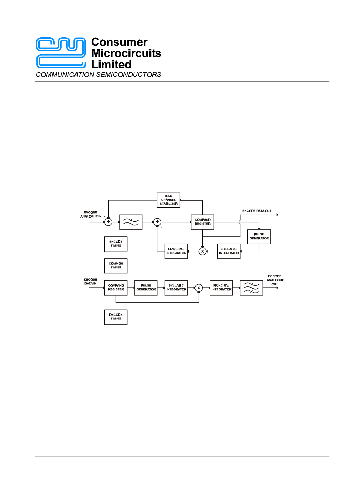
1.2 Block Diagram
Figure 1 Block Diagram
Page 4
CVSD Codec CMX639
2000 Consumer Microcircuits Limited 4 CMX639/2
1.3 Signal List
P6
22-pin
PDIP
E2
24-pin
TSSOP
D4
16-pin
SOIC
Signal Name Type
Description
1 1 1 Xtal/Clock input Input to the clock oscillator inverter. A
1.024MHz Xtal input or externally derived clock
is injected here.
2 N/C No Connection
2 3 2
Xtal
output The 1.024 MHz output of the clock oscillator
inverter.
3 4 N/C No Connection
4 5 3 Encoder Data
Clock
input/
output
A logic I/O port. External encode clock input or
internal data clock output. Clock frequency is
dependent upon Clock Mode 1 and 2 inputs and
Xtal frequency. Note: No internal pull-up is
provided. See Table 3.
5 6 4 Encoder Output output The encoder digital output. This is a three-state
output whose condition is set by the Data Enable
and
Powersave inputs. See Table 2.
6 7
Not
present
Idle Force Encoder
input When this pin is at a logical '0' the encoder is
forced to an idle state and the encoder digital
output is ‘0101…’, a perfect idle pattern. When
this pin is a logical '1' the encoder encodes as
normal. Internal 1M
Ω pull-up.
7 8 5 Data Enable input Data is made available at the encoder output pin
by control of this input. See Encoder Output pin.
Internal 1 M
Ω pull-up.
8 9 N/C No Connection
9 10 6 V
BIAS
Normally at V
DD
/2, this pin should be externally
decoupled by capacitor C4. Internally pulled to
V
SS
when Powersave is a logical '0'.
10 11 7 Encoder Input input The analog signal input. Internally biased at
V
DD
/2, this input requires an external coupling
capacitor. The source impedance driving the
coupling capacitor should be less than 1k
Ω. A
lower driving source impedance will reduce
encoder output channel noise levels.
11 12 8 VSS power Negative Supply
12 13 N/C No Connection
13 14 9 Decoder Output output The recovered analog signal is output at this pin.
It is the buffered output of a lowpass filter and
requires external components. During
‘Powersave’ this output is open circuit.
14 15 N/C No Connection
Page 5
CVSD Codec CMX639
2000 Consumer Microcircuits Limited 5 CMX639/2
P6
22-pin
PDIP
E2
24-pin
TSSOP
D4
16-pin
SOIC
Signal Name Type
Description
15 16 10
Powersave
Input A logic '0' at this pin puts most parts of the codec
into a quiescent, non-operational state. When at a
logical '1', the codec operates normally. Internal 1
M
Ω pull-up.
17 N/C No Connection
16 18
Not
present
Idle
Force Decoder
input A logic '0' at this pin gates a ‘0101...’ pattern
internally to the decoder so that the Decoder
Output goes to V
DD
/2. When this pin is a logical
'1' the decoder operates as normal. Internal 1M
Ω
pull-up.
17 19 11 Decoder Input input
The received digital signal input. Internal 1 M
Ω
pull-up.
18 20 12 Decoder Data
Clock
input/
output
A logic I/O port. External decode clock input or
internal data clock output. Clock frequency is
dependent upon Clock Mode 1 and 2 inputs and
Xtal frequency. Note: No internal pull-up is
provided. See Table 3.
19 21 13 Algorithm input A logic '1' at this pin sets this device for a 3-bit
companding algorithm. A logical '0' sets a 4-bit
companding algorithm. Internal 1 M
Ω pull-up.
20
21
22
23
14
15
Clock Mode 2
Clock Mode 1
input
input
Clock rates refer to f = 1.024MHz Xtal/Clock input.
During internal operation the data clock
frequencies are available at these ports for
external circuit synchronization. Independent or
common data rate inputs to Encode and Decode
data clock ports may be employed in the External
Clocks mode. Internal 1M
Ω pull-ups. See Table 3.
22 24 16 VDD power Positive Supply. A single 3.0V to 5.5V supply is
required. This pin should be externally decoupled
to V
SS
by capacitor C5.
Page 6

CVSD Codec CMX639
2000 Consumer Microcircuits Limited 6 CMX639/2
1.4 External Components
Figure 2 Recommended External Connections
R1 Note 1
1M
Ω ±10%
C4 Note 4
1.0
µF ±20%
C1 Note 2 33pF
±20%
C5 Note 5
1.0
µF ±20%
C2 Note 2 33pF
±20%
X1 Note 6, 7 1.024MHz
C3 Note 3
1.0
µF ±20%
Table 1 Recommended External Components
Notes:
1. Oscillator inverter bias resister
2. Xtal circuit load capacitor
3. The drive source impedance connected to the coupling capacitor’s input node, rather than the CMX639
ENCODER INPUT pin node, should be should be less than 1k
Ω. Output idle channel noise levels will
improve with even lower source impedances driving the coupling capacitor’s input node.
4. Bias decoupling capacitor
5. V
DD
decoupling capacitor
6. A 1.024MHz Xtal/Clock input will yield exactly 16kbps/32kbps/64kbps internally generated data clock rates
7. For best results, a crystal oscillator design should drive the clock inverter input with signal levels of at least
40% of V
DD
, peak to peak. Tuning fork crystals generally cannot meet this requirement. To obtain crystal
oscillator design assistance, please consult your crystal manufacturer.
Page 7

CVSD Codec CMX639
2000 Consumer Microcircuits Limited 7 CMX639/2
1.5 General Description
Data Enable
Powersave
Encoder Output
1 1 Enable
0 don't care High Z (open circuit)
1 0 VSS
Table 2 Encoder Output
Clock Mode 1 Clock Mode 2
Data/Sampling Clock Rate
(CLOCK/XTAL = f = 1.024MHz)
Example for f = 1.024MHz
0 0 External Clocks External Clocks
0 1 Internally generated @ f/16 Internally generated @ 64kbps
1 0 Internally generated @ f/32 Internally generated @ 32kbps
1 1 Internally generated @ f/64 Internally generated @ 16kbps
Table 3 Clock Modes and Pins
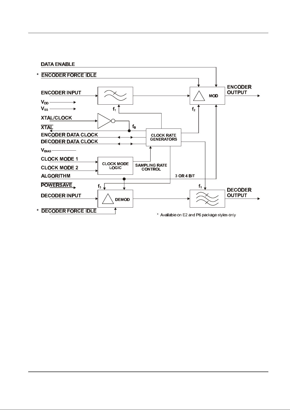
1.6 Application Notes
Figure 3 System Configuration using the CMX639
Page 8

CVSD Codec CMX639
2000 Consumer Microcircuits Limited 8 CMX639/2
1.7 Performance Specification
1.7.1 Electrical Performance
1.7.1.1 Absolute Maximum Ratings
Exceeding these maximum ratings can result in damage to the device.
Min. Max. Units
Supply (VDD - VSS) -0.3 7.0 V
Voltage on any pin to VSS -0.3 V
DD
+ 0.3 V
Current into or out of VDD and V
SS
pins -30 +30 mA
Current into or out of any other pin -20 +20 mA
P6 Package Min. Max. Units
Total Allowable Power Dissipation at Tamb = 25°C 800 mW
... Derating 10 mW/°C
Storage Temperature -40 +125 °C
Operating Temperature -40 +85 °C
E2 Package Min. Max. Units
Total Allowable Power Dissipation at Tamb = 25°C 300 mW
... Derating 3.0 mW/°C
Storage Temperature -40 +125 °C
Operating Temperature -40 +85 °C
D4 Package Min. Max. Units
Total Allowable Power Dissipation at Tamb = 25°C 800 mW
... Derating 10 mW/°C
Storage Temperature -40 +125 °C
Operating Temperature -40 +85 °C
1.7.1.2 Operating Limits
Correct operation of the device outside these limits is not implied.
Notes Min. Max. Units
Supply (VDD - VSS) 2.7 5.5 V
Operating Temperature -40 +85 °C
Xtal Frequency 0.500 2.048 MHz
Page 9

CVSD Codec CMX639
2000 Consumer Microcircuits Limited 9 CMX639/2
1.7.1.3 Operating Characteristics
For the following conditions unless otherwise specified:
Xtal Frequency = 1.024 MHz, Sample Clock Rate = 32 kbps, Audio Test Frequency = 820 Hz,
V
DD
= 3.0V to 5.5V, Tamb = - 40°C to +85°C, Audio Level 0dB ref (0dBm0) = 489mV rms.
Static Values Notes Min. Typ. Max. Units
IDD (powersaved) 6
600
µA
IDD (enabled) @ VDD = 3.0V 6
1.90
mA
I
DD
(enabled) @ VDD = 5.0V 6
2.75
mA
Input Logic ‘1’
70% V
DD
V
Input Logic ‘0’
30% VDD V
Output Logic ‘1’
80% VDD
V
Output Logic ‘0’
20% VDD V
Digital Input Impedance
Logic I/O pins
1.0
M
Ω
Logic Input pins, Pull-up Resistor 1 300
k
Ω
Digital Output Impedance
4.0
k
Ω
Analog Input Impedance 2
100
k
Ω
Analog Output Impedance
800
Ω
Three State Output Leakage
±4
µA
Insertion Loss 3
0 dB
Page 10

CVSD Codec CMX639
2000 Consumer Microcircuits Limited 10 CMX639/2
Dynamic Values Notes Min. Typ. Max. Units
Encoder:
Analog Signal Input Levels
V
DD
= 3.0V 7 -37 6 dB
V
DD
= 5.0V 7 -33 10 dB
Principal Integrator Frequency
160 Hz
Encoder Passband 4
3240 Hz
Compand Time Constant
5 ms
Decoder:
Analog Signal Output Levels
V
DD
= 3.0V 7 -37 6 dB
V
DD
= 5.0V 7 -33 10 dB
Decoder Passband 4
3200 Hz
Encoder Decoder (Full Codec):
Passband 4 300
3400 Hz
Stopband
6 10 kHz
Stopband Attenuation
60 dB
Passband Gain
0 dB
Passband Ripple
-3.0 3.0 dB
Output Noise (Input Short Circuit) 8
-60 dBm0p
Perfect Idle Channel Noise
(Encode Forced) 8, 9
-63 dBm0p
Group Delay Distortion 5
(1000Hz - 2600Hz)
450
µs
(600Hz - 2800Hz)
750
µs
(500Hz - 3000Hz)
1500
µs
Xtal/Clock Frequency
10, 11 0.500 1.024 2.048 MHz
Notes:
1. All logic inputs except Encoder and Decoder Data clocks.
2. The source impedance driving the coupling capacitor should be less than 1k
Ω. A lower driving source
impedance will reduce encoder output channel noise levels.
3. For an Encoder/Decoder combination.
4. See Figure 5.
5. Group Delay Distortion for the full codec is relative to the delay with an 820Hz, -20dB signal at the encoder
input.
6. Not including any current drawn from the device pins by external circuits.
7. Recommended values.
8. dBm0p units are measured after the application of a psophometrically weighted filter that is commonly
applied in voice communication applications per CCITT Recommendation G.223.
9. Forced idle encode/decode control not available on D4 (16-pin SOIC) package.
10. Some applications may benefit from the use of an Xtal/Clock frequency other than 1.024MHz.
Note: Codec time constants and filter response curves are effectively proportional to Xtal/Clock frequency
Page 11

CVSD Codec CMX639
2000 Consumer Microcircuits Limited 11 CMX639/2
and so will shift with the use of Xtal/Clock frequencies other than 1.024MHz. For example, the specified
Encoder Decoder (Full Codec) passband of 300Hz min. to 3400Hz max. for a 1.024MHz Xtal/Clock will
shift to 600Hz min. to 6800Hz max. when the device is operated from a 2.048MHz Xtal/Clock. For this
reason, all CMX639 codecs involved in the same communications link should usually be operated from the
same Xtal/Clock frequency.
Example 1: A design saves the cost of a 1.024MHz Xtal or clock generator by making use of an already
existing clock source of a frequency other than 1.024MHz.
Example 2: Best noise performance is achieved when the CMX639 codec data clock is internally
generated. If a codec bit rate other than 16kbps, 32kbps or 64kbps is desired then an Xtal/Clock different
from 1.024MHz can be used to proportionately shift the available set of internally generated clock rates, as
needed.
Example 3: To increase the codec high frequency response and audio bandwidth a faster Xtal/Clock
speed can be used. Other designs may prefer the proportionately higher codec bandwidths and data rates
that can be supported with faster clock speeds.
11. In general, optimum codec performance is achieved when both encoder and decoder Xtal/Clock signals
are synchronized. While this is practical in many telecom applications, it may not be so for others such as
wireless data links. The CMX639 decoder can generally deliver best performance when its data clock is
recovered/derived from the received data stream and applied as an external data clock to the decoder as
per the decoder timing depicted in Figure 4. Nonetheless, some Xtal/Clock frequency and data rate
combinations are better served by the use of internal clocks. Experimentation with each specific design
may provide the best guidance for making this design choice.
Page 12

CVSD Codec CMX639
2000 Consumer Microcircuits Limited 12 CMX639/2
1.7.1.3 Operating Characteristics (continued)
Timing Diagram
ENCODER TIMING
DECODER TIMING
MULTIPLEXING FUNCTION
ENCODER
CLOCK
ENCODER DATA
OUTPUT
DECODER
CLOCK
DECODER DATA
INPUT
ENCODER
OUTPUT
DATA ENABLE
HIGH Z HIGH Z
DATA TRUE TIME
DATA CLOCKED
DATA CLOCKED
t
IF
t
IR
t
CL
t
CH
t
CH
t
SU
t
H
t
DR
t
PCO
t
DF
Figure 4 Serial Bus Timing
For the following conditions unless otherwise specified:
Xtal Frequency = 1.024 MHz, V
DD
= 3.0V to 5.0V, Tamb = - 40°C to +85°C.
Serial Bus Timing (ref. Figure 4)
Notes Min. Typ. Max. Units
tCH Clock 1 pulse width
1.0
µs
tCL Clock 0 pulse width
1.0
µs
tIR Clock rise time
0 100
ns
tIF Clock fall time
100 ns
tSU Data set-up time
450 ns
tH Data hold time
600
ns
tSU +tH Data true time
1.5
µs
t
PCO
Clock to output delay time
750 ns
tDR Data rise time
100 ns
tDF Data fall time
100 ns
Page 13

CVSD Codec CMX639
2000 Consumer Microcircuits Limited 13 CMX639/2
1.7.1.3 Operating Characteristics (continued)
Typical Codec Performance
0
-10
-20
-30
Input Level = -15dBmO
Data Clocks = 32kbps
Xtal = 1.024MHz
1 2 3 4
5
6
Frequency (kHz)
-40
-50
-60
Codec G ain
including encode and decode, (dB)
Figure 5 Typical Frequency Response (32kbps)
Frequency (Hz)
S/N (dB)
35
30
25
20
15
10
5
500 100015002000250030003500
Input Level = -20dB
64kb/s
32kb/s
16kb/s
Figure 6 Typical S/N Ratio with Input Frequency
Page 14

CVSD Codec CMX639
2000 Consumer Microcircuits Limited 14 CMX639/2
Input Frequency = 820Hz
Input Level (dBmO)
3
2
1
0
-1
-40 -30 -20 -10 0 10
Attenuation (dB )
ref @ -15dBmO
Figure 7 Typical Variation of Gain with
Input Level (32kbps)
S/N (dB )
Input Level (dB)
ref.
-40 -30 -20 -10 0
Ref: 0dB Input Level = 489mVrms
Input Frequency = 820 Hz
64 kbps
32 kbps
16 kbps
10
20
30
35
Figure 8 Typical S/N Ratio with Input Level
Page 15

CVSD Codec CMX639
2000 Consumer Microcircuits Limited 15 CMX639/2
1.7.2 Packaging
Figure 9 P6 Mechanical Outline: Order as part no. CMX639P6
Figure 10 E2 Mechanical Outline: Order as part no. CMX639E2
Page 16

CVSD Codec CMX639
Handling precautions: This product includes input protection, however, precautions should be taken to prevent device damage from
electro-static discharge. CML does not assume any responsibility for the use of any circuitry described. No IPR or circuit patent
licences are implied. CML reserves the right at any time without notice to change the said circuitry and this product specification. CML
has a policy of testing every product shipped using calibrated test equipment to ensure compliance with this product specification.
Specific testing of all circuit parameters is not necessarily performed.
Oval Park - LANGFORD
MALDON - ESSEX
CM9 6WG - ENGLAND
Telephone: +44 (0)1621 875500
Telefax: +44 (0)1621 875600
e-mail: sales@cmlmicro.co.uk
http://www.cmlmicro.co.uk
Figure 9 D4 Mechanical Outline: Order as part no. CMX639D4
 Loading...