

Page 1
DATA BULLETIN
CMX631A
© 1999 MX
•COM Inc. www.mxcom.com Tele: 800 638-5577 336 744-5050 Fax: 336 744-5054 Doc. # 20480177.004
4800 Bethania Station Road, Winston-Salem, NC 27105-1201 USA All trademarks and service marks are held by their respective companies.
Low Voltage
SPM Detector
PRELIMINARY INFORMATION
Features Applications
•
Detects 12kHz or 16kHz SPM
Frequencies
•
Tone Follower and Packet Mode
Outputs
•
High Speech-Band Rejection
Properties
•
Low Power Operation (3.0V < 0.8mA)
•
Call Charge Applications on PABX Line
Cards
•
Complex and/or Simple telephone
Systems
•
Remote Telephone/Payphones
+
-
1
32
PERIOD
MEASURE
TONE
FOLLOWER
LOGIC
PACKET
TONE
LOGIC
DIVIDER
SIGNAL IN (-)
AMP OUT
XTAL/CLOCK
SYSTEM (12kHz/16kHz)
SYSTEM
SYSTEM
CLOCK IN
CLOCK OUT
TONE FOLLOWER
OUTPUT
V
SS
V
DD
V
BIAS
P ACKET MODE
OUTPUT
SIGNAL IN (+)
LEVEL DETECTOR
+20dB
12kHz/16kHz
XTAL
CLOCK
DIVIDERS
INPUT AM P
XTAL/CLOCK
OSCILLATOR
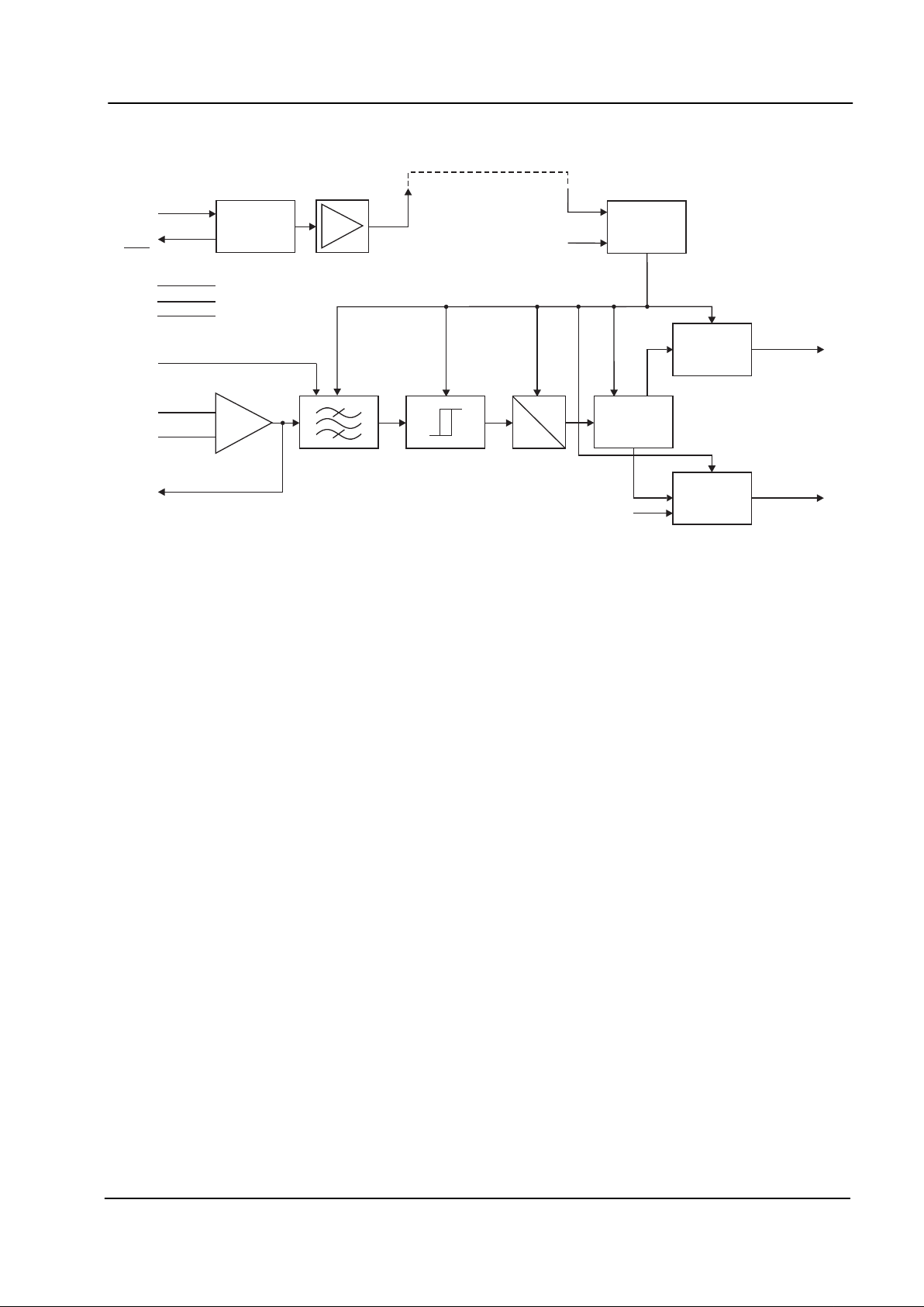
The CMX631A is a low-power, system-selectable Subscriber Pulse Metering (SPM) detector that indicates the
presence of both 12kHz or 16kHz telephone call-charge frequencies on a telephone line.
Deriving its input directly from the telephone line, input amplitude/sensitivities are component adjustable to the
user's national ‘Must/Must-Not Decode’ specifications via an on-chip input amplifier. The 12kHz and 16kHz
frequency limits are accurately defined by the use of an external 3.579545MHz telephone-system Xtal or
clock-pulse input.
The CMX631A demonstrates exceptional 12kHz and 16kHz performance in the presence of both voice and
noise. This device may operate from a single or differential analog signal input, from which two individual
logic outputs will be produced; a Tone Follower Output or a Packet Mode Output.
This system (12kHz/16kHz) selectable integrated circuit, requires a 2.7V to 5.5V power supply, which may be
line-powered, is available in the following packages: 24-pin SSOP (CMX631AD5), 16-pin SOIC
(CMX631AD4), and 16-pin PDIP (CMX631AP3). Additional package styles may be available to meet specific
design requirements.
Page 2

Low Voltage SPM Detector 2 CMX631A PRELIMINARY INFORMATION
© 1999 MX•COM Inc. www.mxcom.com Tele: 800 638-5577 336 744-5050 Fax: 336 744-5054 Doc. # 20480177.004
4800 Bethania Station Road, Winston-Salem, NC 27105-1201 USA All trademarks and service marks are held by their respective companies.
CONTENTS
Section Page
1 Block Diagram................................................................................................................3
2 Signal List.......................................................................................................................4
3 External Components....................................................................................................5
4 General Description.......................................................................................................6
4.1 Tone Follower Mode............................................................................................................ 6
4.2 Packet Mode........................................................................................................................ 6
4.3 Sensitivity Setting ................................................................................................................ 6
4.3.1 Input Gain Calculation............................................................................................................6
4.3.2 Input Gain Components .........................................................................................................8
4.4 ‘WILL’/’WILL-NOT’ Detect Frequencies............................................................................... 8
5 Applications ...................................................................................................................8
5.1 Input Configurations ............................................................................................................ 8
5.1.1 Protection Against High Voltages...........................................................................................8
5.1.2 Aliasing...................................................................................................................................9
6 Performance Specification............................................................................................9
6.1 Electrical Specifications....................................................................................................... 9
6.1.1 Absolute Maximum Ratings....................................................................................................9
6.1.2 Operating Limits...................................................................................................................10
6.1.3 Operating Characteristics.....................................................................................................10
6.2 Packages........................................................................................................................... 11
MX-COM, Inc. reserves the right to change specifications at any time and without notice.
Page 3
Low Voltage SPM Detector 3 CMX631A PRELIMINARY INFORMATION
© 1999 MX•COM Inc. www.mxcom.com Tele: 800 638-5577 336 744-5050 Fax: 336 744-5054 Doc. # 20480177.004
4800 Bethania Station Road, Winston-Salem, NC 27105-1201 USA All trademarks and service marks are held by their respective companies.
1 Block Diagram
+
-
1
32
PERIOD
MEASURE
TONE
FOLLOWER
LOGIC
PACKET
TONE
LOGIC
DIVIDER
SIGNAL IN (-)
AMP OUT
XTAL/CLOCK
SYSTEM (12kHz/16kHz)
SYSTEM
SYSTEM
CLOCK IN
CLOCK OUT
TONE FOLLOWER
OUTPUT
V
SS
V
DD
V
BIAS
P ACKET MODE
OUTPUT
SIGNAL IN (+)
LEVEL DETECTOR
+20dB
12kHz/16kHz
XTAL
CLOCK
DIVIDERS
INPUT AM P
XTAL/CLOCK
OSCILLATOR
Figure 1: Block Diagram
Page 4
Low Voltage SPM Detector 4 CMX631A PRELIMINARY INFORMATION
© 1999 MX•COM Inc. www.mxcom.com Tele: 800 638-5577 336 744-5050 Fax: 336 744-5054 Doc. # 20480177.004
4800 Bethania Station Road, Winston-Salem, NC 27105-1201 USA All trademarks and service marks are held by their respective companies.
2 Signal List
Packages Signal
D5 D4/P3 Name Type
Description
1 1 Xtal/Clock input The input to the on-chip clock oscillator; for use with a
3.579545MHz Xtal in conjunction with the Xtal output; circuit
components are on-chip. When using a Xtal input, the Clock
Out pin should be connected directly to the Clock In pin. If a
clock pulse input is used at the Clock In pin, this (Xtal/Clock)
pin must be connected directly to V
DD
See Figure 2 and
Section 3.
42
XTAL
output The output of the on-chip clock oscillator inverter.
5 3 Clock Out output The buffered output of the on-chip-clock oscillator inverter. If a
Xtal input is used, this output should be connected directly to
the Clock In pin.
6 4 Clock In input The 3.579545MHz clock pulse input to the internal clock
dividers. If an externally generated clock pulse is used, the
Xtal/Clock input pin should be connected to V
DD
. Reference
Section 3.
87V
BIAS
power The output of the on-chip analog bias circuitry. Held internally
at V
DD
/2, this pin should be bypassed to VSS. See Figure 2.
12 8 V
SS
power Negative supply (GND).
13 9 Signal In + input The positive input to the input gain adjusting signal amplifier.
Reference Section 4.3 and 4.4.
17 10 Signal In - input The negative input to the input gain adjusting signal amplifier.
Reference Section 4.3 and 4.4.
18 11 Amp Out input The output of the input gain adjusting signal amplifier.
Reference Section 4.3 and 4.4.
19 13 Tone
Follower
Mode
output This output provides a logic 0 for the period of a detected tone
and a logic 1 for a NOTONE detection. See Section 4.1 and
Figure 3.
20 14 Packet Mode output This output provides a logic 0 for a detected tone and a logic 1
for NOTONE detection and will ignore a small fluctuation or
fade during the tone signal. See Section 4.2 and Figure 3.
21 15 System input This logic input selects the device operation to either 12kHz
(logic 1) or 16kHz (logic 0) SPM systems. This input has an
internal 1MΩ pull-up resistor (12kHz).
24 16 V
DD
power Positive supply. A single, stable power supply is required.
Critical levels and voltages within the CMX631A are dependent
upon this supply. This pin should be bypassed to V
SS
by a
capacitor mounted close to the pin. Note: If this device is line
powered, the resulting power supply must be stable. See
Section 5.1.1.
2, 3, 7,
9, 10,
11, 14,
15, 16,
22, 23
5,6,12 N/C No internal connection; leave open circuit.
Table 1: Signal List
Page 5

Low Voltage SPM Detector 5 CMX631A PRELIMINARY INFORMATION
© 1999 MX•COM Inc. www.mxcom.com Tele: 800 638-5577 336 744-5050 Fax: 336 744-5054 Doc. # 20480177.004
4800 Bethania Station Road, Winston-Salem, NC 27105-1201 USA All trademarks and service marks are held by their respective companies.
3 External Components
V
DD
C1
C2
C4
C3
R4
R3
R2
R1
V
SS
V
BIAS
1
2
3
4
5
6
7
8
16
15
14
13
12
11
10
9
TONE FOLLOWER OUTPUT
PACKET MODE OUTPUT
SYSTEM
CLOCK IN
SIGNAL IN (+)
SIGNAL IN (-)
AMP OUT
X1
XTAL/CLOCK
CLOCK OUT
XTAL
CMX631A
D4/P3
V
DD
Figure 2: Recommended External Components
R1 Note 1 R
FEEDBACK
C1 1.0µF ±20%
R2 Note 1 R
IN(-)
C2 1.0µF ±20%
R3 Note 1 R
IN(+)
C3 C
IN(-)
R4 Note 1 R
BIAS
C4 C
IN(+)
X1 Note 2, 3, 4 3.579545MHz
Table 2: Recommended External Components
Recommended External Component Notes:
1. When calculating input gain components, for correct operation R1 and R4 should always be ≥ 33kΩ.
2. For best results, a crystal oscillator design should drive the clock inverter input with signal levels of at
least 40% of V
DD
, peak to peak. Tuning fork crystals generally cannot meet this requirement. To
obtain crystal oscillator design assistance, consult your crystal manufacturer.
3. The on-chip crystal circuitry includes a feedback resistor (nominally 2MΩ) between pins 1 and 2 and
load capacitors on pins 1 and 2 (nominally 10pF each, excluding package and board parasitics).
4. When using an external clock input, X1 should be removed, Pin 1 (Xtal/Clock) should be tied to VDD,
the Clock In and Clock Out jumper should be removed, and the external clock signal applied to Clock
In.
Page 6

Low Voltage SPM Detector 6 CMX631A PRELIMINARY INFORMATION
© 1999 MX•COM Inc. www.mxcom.com Tele: 800 638-5577 336 744-5050 Fax: 336 744-5054 Doc. # 20480177.004
4800 Bethania Station Road, Winston-Salem, NC 27105-1201 USA All trademarks and service marks are held by their respective companies.
4 General Description
4.1 Tone Follower Mode
The Tone Follower Output Mode will respond and/or de-respond when a signal is detected or a NOTONE, by
providing a Logic level output. When a signal has been detected, a Logic 0 is provided at the output for the
duration of the valid signal. When a NOTONE or invalid decode is detected a Logic 1 is provided at the
output until a valid signal is available. See Figure 3.
4.2 Packet Mode
The Packet (Cumulative Tone) Mode Output will respond and/or de-respond after a cumulative 40ms of good
tone (or NOTONE) in any 48ms period by providing a Logic level output. See Figure 3.
This process does ignore the small fluctuations or fades of a valid frequency input. During a 40ms toneburst,
no tone interruption (small fluctuation or fade) is allowed during this period for the signal to be considered
valid. If a 45ms toneburst occurs, then a 2ms interruption is allowed, and the signal is still considered valid.
For NOTONE, there must be 40ms of continuous no tone or for a 45ms period, there may be 2ms of tone and
the NOTONE still be valid. For a valid detect of tone the output provides a Logic 0. For the valid detect of
NOTONE, the output provides a Logic 1.
This output is available for µProcessor ‘Wake-Up’, Minimum Tone detection, NOTONE indication, or transient
avoidance.
SIGNAL INPUT
RESPONSE DELAY
TONE FOLLOWER OUTPUT
P ACKET MODE OUTPUT
DERESPONSE DELAY
SIGNAL INPUT
P ACKET MODE OUTPUT
TONE FOLLOWER OUTPUT
RESPONSE DELAY
De-response
Response
DERESPONSE DELAY
Figure 3: Tone Follower and Packet Mode Outputs
4.3 Sensitivity Setting
The CMX631A input sensitivity can be accurately adjusted and set to support many national 12kHz and
16kHz SPM specifications.
4.3.1 Input Gain Calculation
The input amplifier, with external circuitry, is used to set the sensitivity of the CMX631A to conform to the
user's national level specification with regard to ‘Must’ and ‘Must-Not’ decode signal levels.
With reference to the graphs in Figure 4 and Figure 5, the following steps will assist in the determination of the
required gain/attenuation.
1. Draw two horizontal lines from the Y-axis [Signal Level (dB)] in Figure 4 and Figure 5. The upper line
represents the required ‘Must’ decode level. The lower line represents the required ‘Must-Not’ decode
level
Page 7

Low Voltage SPM Detector 7 CMX631A PRELIMINARY INFORMATION
© 1999 MX•COM Inc. www.mxcom.com Tele: 800 638-5577 336 744-5050 Fax: 336 744-5054 Doc. # 20480177.004
4800 Bethania Station Road, Winston-Salem, NC 27105-1201 USA All trademarks and service marks are held by their respective companies.
2. Mark the intersection of the upper horizontal line and the upper sloping line; drop a vertical line from this
point to the X-axis [Amplifier Gain (dB)]. The point where the vertical line meets the X-axis indicates the
minimum Input Amp gain required for reliable decoding of valid signals.
3. Mark the intersection of the lower horizontal line and the lower sloping line; drop a vertical line from this
point to the X-axis. The point where the vertical line meets the X-axis will indicate the maximum allowable
Input Amp gain. Input signals at or below the ‘Must-Not’ decode level will not be detected as long as the
amplifier gain is no higher than this level.
-5 0
-4 0
-3 0
-2 0
-1 0
-3 0 -2 0 -1 0 0 10 20 30
MUST DECODE LEVEL
MUST NOT DECODE LEVEL
MAXIMUMAMPLIFIER GAINMINIMUM AMPLIFIER GAIN
AMPLIFIER GAIN (dB) V = 3.0V (±0.1) T = -40°C to 85°C
DD AMB
SIGNAL LEVEL (dB) 0dB ref: 775mV
RMS
Figure 4: Input Gain Calculation Graph for VDD = 3.0V
-50
-45
-40
-35
-30
-25
-20
-15
-10
-25 -20 -15 -10
-5
0
5
10 15 20 25
MUST DECODE LEVEL
MUST NOT DECODE LEVEL
AMPLIFIER GAIN (dB) V = 5.0 (±0.5) TEMP = -40°C to 85°C
DD
SIGNAL LEVEL (dB) 0dB ref: 775mV
RMS
MINIMUM AM P L IF IE R GAIN MAXIMUM AMPLIFIER G AIN
Figure 5: Input Gain Calculation Graph for VDD = 5.0V
Page 8

Low Voltage SPM Detector 8 CMX631A PRELIMINARY INFORMATION
© 1999 MX•COM Inc. www.mxcom.com Tele: 800 638-5577 336 744-5050 Fax: 336 744-5054 Doc. # 20480177.004
4800 Bethania Station Road, Winston-Salem, NC 27105-1201 USA All trademarks and service marks are held by their respective companies.
4.3.2 Input Gain Components
Reference the gain components found in Table 2 and Figure 2. The user should calculate and select external
components (R1/R3/C3 and R2/R4/C4) to provide amplifier gain within the limits obtained in Section 4.3.1.
Component tolerances should not move the gain-figure outside these limits. The graphs in Figure 4 and
Figure 5 are for the calculation of input gain components for a CMX631A using a V
DD
of 3.0 (±0.1) or VDD of
5.0 (±0.5).
4.4 ‘WILL’/’WILL-NOT’ Detect Frequencies
16.00kHz
15.76kHz
15.36kHz
F-4%
0
F+4%
0
F - 1.5%
0
F + 1.5%
0F0
16.24kHz
16.64kHz
12.00kHz
11.82kHz
11.52kHz
F-4%
0
F+4%
0
F - 1.5%
0
F + 1.5%
0F0
12.18kHz
12.48kHz
WILL-NOT DETECT
FREQUENCIES
WILL-NOT DETECT
FREQUENCIES
WILL-NOT DETECT
FREQUENCIES
WILL-NOT DETECT
FREQUENCIES
WILL DETECT
FREQUENCIES
WILL-DETECT
FREQUENCIES
Figure 6: ‘WILL’/’WILL-NOT’ Detect Frequencies
5 Applications
5.1 Input Configurations
+
-
INPUT AMP
V
BIAS
+
-
Tip (a)
Ring (b)
INPUT AMP
CMX631A
V
BIAS
Differential Input
Common Mode Input
CMX631A
Figure 7: Input Configurations
5.1.1 Protection Against High Voltages
Telephone systems may have high DC and AC voltages present on the line. If the CMX631A is a part of host
equipment that has its own signal input protection circuitry, there will be no need for further protection as long
as the voltage on any pin is limited to within V
DD
+0.3V and VSS -0.3V.
If the host system does not have input protection, or there are signals present outside the device's specified
limits, the CMX631A will require protection diodes at its signal inputs (+ and -). The breakdown voltage of
capacitors and the peak inverse voltage of the diodes must be sufficient to withstand the sum of the DC
voltages plus all expected signal peaks.
Page 9

Low Voltage SPM Detector 9 CMX631A PRELIMINARY INFORMATION
© 1999 MX•COM Inc. www.mxcom.com Tele: 800 638-5577 336 744-5050 Fax: 336 744-5054 Doc. # 20480177.004
4800 Bethania Station Road, Winston-Salem, NC 27105-1201 USA All trademarks and service marks are held by their respective companies.
5.1.2 Aliasing
Due to the sampling nature of switched-capacitor filters used in the CMX631A, high frequency noise or
unwanted signals can alias into the passband, disrupting detection. External components must be chosen
carefully to avoid alias effects.
Possible Alias Frequencies:
12kHz Mode = 52kHz
16kHz Mode = 69kHz
If other filtering in the system has not attenuated these alias frequencies, capacitors should be employed
across resistors R1 and R4 to provide anti-alias filtering.
The low-pass cutoff frequency should be chosen to be approximately 20kHz to 25kHz for a 12kHz system, or
25kHz to 30kHz for a 16kHz system.
i.e.
)4R or 1R(×f××2
1
=C
0
When anti-alias capacitors are used, an allowance must be made for reduced gain at the SPM frequency
(12kHz or 16kHz).
6 Performance Specification
6.1 Electrical Specifications
6.1.1 Absolute Maximum Ratings
Exceeding the maximum rating can result in device damage.
Parameter Min. Typ. Max. Unit
Supply Voltage (VDD-VSS) -0.3 7.0 V
Voltage on any pin to V
SS
-0.3 (VDD + 0.3) V
Current
V
DD
-30 30 mA
V
SS
-30 30 mA
Any other pin -20 20 mA
D4 / P3 Packages
Total allowable device dissipation at T
AMB
25°C
800 mW
Derating above T
AMB
25°C
13
mW/°C above T
AMB
25°C
Operating Temperature -40 85
°
C
Storage Temperature -40 85
°
C
D5 Package
Total allowable device dissipation at T
AMB
25°C
550 mW
Derating above T
AMB
25°C
9
mW/°C above T
AMB
25°C
Operating Temperature -40 85
°
C
Storage Temperature -40 85
°
C
Page 10

Low Voltage SPM Detector 10 CMX631A PRELIMINARY INFORMATION
© 1999 MX•COM Inc. www.mxcom.com Tele: 800 638-5577 336 744-5050 Fax: 336 744-5054 Doc. # 20480177.004
4800 Bethania Station Road, Winston-Salem, NC 27105-1201 USA All trademarks and service marks are held by their respective companies.
6.1.2 Operating Limits
Correct Operation of the device outside these limits is not implied.
Parameter Min. Typ. Max. Unit
Supply Voltage (VDD) 2.7 3.0/5.0 5.5 V
Operating Temperature -40 85
Xtal/Clock Frequency 3.558918 3.589368 MHz
6.1.3 Operating Characteristics
All device characteristics are measured under the following conditions unless otherwise specified:
V
DD
= 3.0V to 5.0V @ T
AMB
= -40°C to 85°C
Audio Level 0dB (ref.) = 775mV
RMS
, Noise Bandwidth = 50kHz
Xtal/Clock Frequency = 3.579545MHz, System Setting = 12kHz or 16kHz
Notes Min. Typ. Max. Units
Supply Current
VDD = 3.0V 0.8 mA
VDD = 5.0V 2.2 mA
Logic Inputs/Outputs
Input Logic ‘1’ 70 %V
DD
Input Logic ‘0’ 30 %V
DD
Output Logic ‘1’ 90 %V
DD
Output Logic ‘0’ 10 %V
DD
Xtal/Clock or Clock In Frequency
3.558918 3.589368 MHz
External Clock Pulse Width
High 100 ns
Low 100 ns
Input Amplifier
D. C. Gain 60.0 dB
Bandwidth (-3dB) 100 Hz
Input Impedance 1.0
M
Ω
Logic Impedances
Input
System 0.7 3.8
M
Ω
Clock In 10.0
M
Ω
Output 14.0 30.0
k
Ω
Overall Performance
12kHz Detect Bandwidth 1 11.820 12.180 kHz
12kHz Not-detect Frequencies (below 12kHz) 1 11.520 kHz
12kHz Not-detect Frequencies (above 12kHz) 1 12.480 kHz
16kHz Detect Bandwidth 1 15.760 16.240 kHz
16kHz Not-detect Frequencies (below 16kHz) 1 15.360 kHz
16kHz Not-detect Frequencies (above 16kHz) 1 16.640 kHz
Sensitivity
VDD = 3.0V±0.1V
2 -27.8 -31.8 dBm
VDD = 5.0V±0.5V
2 -23.5 -27.5 dBm
Page 11

Low Voltage SPM Detector 11 CMX631A PRELIMINARY INFORMATION
© 1999 MX•COM Inc. www.mxcom.com Tele: 800 638-5577 336 744-5050 Fax: 336 744-5054 Doc. # 20480177.004
4800 Bethania Station Road, Winston-Salem, NC 27105-1201 USA All trademarks and service marks are held by their respective companies.
Tone Operating Characteristics
Signal-to-Noise Requirements (Amp Input) 3, 4, 5, 6 22.0 20.0 dB
Signal-to-Voice Requirements (Amp Input) 3, 4, 5, 7 -36.0 -40.0 dB
Signal-to-Voice Requirements (Amp Output) 5, 6 -25.0 -29.0 dB
Tone Follower Mode 1, 8
Response and De-Response Time 10.0 ms
Packet Mode 1, 8
Response and De-Response Time 40.0 48.0 ms
Table 3: Operating Characteristics
Operating Characteristics Notes:
1. With adherence to Signal-to-Voice and Signal-to-Noise specifications.
2. With Input Amplifier gain set to unity gain. Reference Section 4.3 for description of sensitivity setting.
3. Common Mode SPM and balanced voice signal.
4. Immune to false responses.
5. Immune to false de-responses.
6. With SPM and voice signal amplitudes balanced. To avoid false de-responses due to saturation, the
peak to peak voice+noise level at the output of the Input Amp (12/16kHz Filter Input) should be no
greater than the dynamic range of the device.
7. Maximum voice frequencies = 3.4kHz.
8. Response, De-Response, and Power-up Response timing.
6.2 Packages
The CMX631A is available in the following packages. Additional package styles may be available to meet
specific design requirements.
NOTE: Alldimensions in inche s(mm.)
Angles are in degrees
PackageTolerances
A
B
C
E
H
TYP.
MAX.MIN.
DIM.
J
P
X
T
Y
Z
L
0.079 (2.00)0.066 (1.67)
0.312 (7.90)
0°
7°
4°
8°
9°
10°
0.037 (0.95)
0.328 (8.33)
0.213 (5.39)
0.026 (0.65)
0.022 (0.55)
0.301 (7.65)
0.008 (0.21)0.002 (0.05)
0.005 (0.13) 0.009 (0.22)
0.010 (0.25) 0.015 (0.38)
0.318 (8.07)
0.205 (5.20)
X
C
H
P
J
Y
E
Z
L
T
PIN 1
A
B
Figure 8: 24-pin SSOP Mechanical Outline:
order as part no. CMX631AD5
Page 12

Low Voltage SPM Detector 12 CMX631A PRELIMINARY INFORMATION
© 1999 MX•COM Inc. www.mxcom.com Tele: 800 638-5577 336 744-5050 Fax: 336 744-5054 Doc. # 20480177.004
4800 Bethania Station Road, Winston-Salem, NC 27105-1201 USA All trademarks and service marks are held by their respective companies.
PIN 1
A
B
ALTERNATIVE
PIN
LOCATION
MARKING
X
P
J
Y
C
K
H
E
L
T
W
Z
NOTE: Alldimensions in inches(mm.)
Angles are in degrees
PackageTolerances
A
B
C
E
H
TYP.
MAX.MIN.
DIM.
J
P
X
W
T
Y
K
L
0.105 (2.67)0.093 (2.36)
0.419 (10.64)
45°
7°
0° 10°
0.050 (1.27)
0.041 (1.04)
0.413 (10.49)
0.299 (7.59)
0.050 (1.27)
0.016 (0.41)
0.390 (9.90)
0.020 (0.51)0.003 (0.08)
0.009 (0.23) 0.0125 (0.32)
0.013 (0.33) 0.020 (0.51)
0.395 (10.03)
0.286 (7.26)
Z
5°
5°
Figure 9: 16-pin SOIC Mechanical Outline:
order as part no. CMX631AD4
PackageTolerances
NOTE: Alldimensions in inche s(mm.)
Angles are in degrees
TYP. MAX.MIN.
A
B
C
E
E1
H
DIM.
J
J1
P
Y
T
K
L
0.200 (5.06)
0.262 (6.63)
0.390 (9.91).
7°
0.150 (3.81)
0.810 (20.57)
0.135 (3.43)
0.100 (2.54)
0.121 (3.07)
0.300 (7.62)
0.290 (7.37) 0.325 (8.26)
0.015 (0.38) 0.070 (1.77)
0.008 (0.20) 0.015 (0.38)
0.014 (0.35) 0.023 (0.58)
0.040 (1.02) 0.065 (1.65)
0.056 (1.42) 0.064 (1.63)
0.740 (18.80)
0.240 (6.10)
B
A
PIN 1
E
Y
E1
T
K
H
J1
J
C
P
L
Figure 10: 16-pin PDIP Mechanical Outline:
order as part no. CMX631AP3
 Loading...