

Page 1
CMX624
D/624/6 January 2001 Provisional Information
V.23/Bell 202 Modem
Features Applications
•• V.23 / Bell 202 Compatible Modem •• Telephone Telemetry Systems
•• Integrated DTMF Encoder •• Remote Utility Meter Reading
•• Call Progress Tone Detection •• Security Systems/Cash Terminals
•• Line Reversal and Ring Detector •• Industrial Control Systems
•• Low Power Operation (2.7V) •• Pay-Phones
•• Part of the CMX6x4 Modem Series •• Cable TV Set-Top Boxes
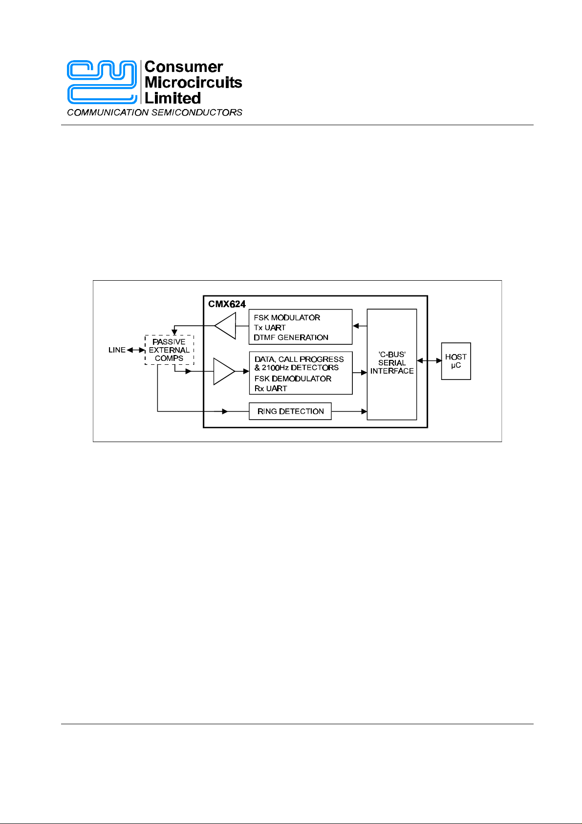
1.1 Brief Description
The CMX624 V.23 / Bell 202 modem is intended for use in any telephone based information and telemetry
system with low power requirements. Using FSK signalling, fast call set-up times and robust error resistant
transmission can be implemented by efficient low power circuits. The circuit can operate at 1200bps full
duplex over a 4-wire circuit or 1200 bps plus low speed data over a 2-wire circuit. Flexible line driver and
receive hybrid circuitry are integrated on chip requiring only passive external components to build a 2- or 4wire interface. A low impedance pull down output is provided for a hook relay.
Control of the device is via a simple high speed serial bus; this allows easy interfacing to a host µController.
The data transmitted and received by the modem is also transferred over the same high speed serial bus. Onchip programmable Tx and Rx UARTs allow asynchronous data to be simultaneously encoded and decoded.
Either UART may be disabled to allow 8-bit raw data to be received or transmitted. Any repetitive 8-bit data
pattern can be sent without the controller having to reload data every 8 bits. All 16 DTMF combinations are
available along with a single tone 'melody' mode. The ringing, 2100Hz, call progress and data detectors
included on the CMX624 make the set-up of a telephone call a simple matter for the host µController.
In many data collection and telemetry systems low power consumption is important. The CMX624 features a
'Zero Power' standby mode. Whilst in standby the ring detector continues to operate and will supply the host
µController with an interrupt when line reversal or ringing is detected. The CMX624 can operate on a supply
voltage between 3.0V and 5.5V across the full temperature range of -40°C to +85°C.
The CMX624 is pin compatible with the CMX644A V22 and Bell 212A modem also from CML.
2001 Consumer Microcircuits Limited
Page 2

V23 / Bell 202 Modem CMX624
CONTENTS
Section
Page
1.1 Brief Description .......................................................................................1
1.2 Block Diagram ...........................................................................................3
1.3 Signal List...................................................................................................4
1.4 External Components...............................................................................6
1.5 General Description..................................................................................6
1.5.1 Xtal Osc and Clock Dividers.......................................................6
1.5.2 Rx Input Amplifier........................................................................7
1.5.3 Receive Filter and Equaliser.......................................................7
1.5.4 FSK Demodulator.........................................................................8
1.5.5 Rx Energy Detector .....................................................................8
1.5.6 FSK / DTMF Modulator ................................................................8
1.5.7 Transmit Filter ..............................................................................9
1.5.8 Transmit Output Buffer.............................................................10
1.5.9 Ring Signal Detector..................................................................10
1.5.10 Tx/Rx UART.................................................................................11
1.5.11 ‘C-BUS’ Interface........................................................................13
1.5.12 ‘C-BUS’ Registers......................................................................14
1.6 Application Notes....................................................................................14
1.6.1 Line Interface..............................................................................15
1.6.2 Ring Detector Interface.............................................................17
1.7 Performance Specification.....................................................................19
1.7.1 Electrical Performance..............................................................19
1.7.2 Packaging....................................................................................24
Note: This product is in development: Changes and additions will be made to this specification. Items
marked TBD or left blank will be included in later issues.
2001 Consumer Microcircuits Limited 2 D/624/6
Page 3
V23 / Bell 202 Modem CMX624
1.2 Block Diagram
Figure 1 Block Diagram
2001 Consumer Microcircuits Limited 3 D/624/6
Page 4

V23 / Bell 202 Modem CMX624
1.3 Signal List
CMX624
D2/D5/P4
Pin No. Name Type
1 XTALN O/P The output of the on-chip Xtal oscillator inverter.
2 XTAL/CLOCK I/P The input to the oscillator inverter from the Xtal
3 SERIAL
4 COMMAND
Signal Description
circuit or external clock source.
CLOCK
I/P
The ‘C-BUS’ serial clock input from the µC. See
Section 1.5.11
DATA
I/P
The ‘C-BUS’ serial data input from the µC.
5 REPLY DATA T/S
A 3-state ‘C-BUS’ serial data output to the µC.
This output is high impedance when not sending
data to the
µC.
6 CSN I/P The ‘C-BUS’ transfer control input provided by
µC.
the
7 IRQN O/P
A ‘wire-ORable’ output for connection to a µC
Interrupt Request input. This output is pulled
down to Vss when active and is high impedance
when inactive. An external pullup resistor is
required.
8 TOP O/P The Tx analogue signal output.
9 TXO O/P The output of the line driving amplifier.
10 TXN I/P The inverting input to the line driver amplifier.
11 TXON O/P The inverted output of the line driving amplifier.
12 V
13 V
Power The negative supply rail (ground).
SS
O/P Internally generated bias voltage of V
BIAS
DD
/2,
except when the device is in ‘Zero Power’ mode
when V
decoupled to V
will discharge to VSS. Should be
BIAS
by a capacitor mounted close
SS
to the device pins.
14 RLYDRV O/P Relay drive open drain output. This output is
pulled down to V
when active and is high
SS
impedance when inactive.
15 RXP I/P The non-inverting input to the Rx input amplifier.
2001 Consumer Microcircuits Limited 4 D/624/6
Page 5

V23 / Bell 202 Modem CMX624
CMX624
D2/D5/P4
Signal Description
Pin No. Name Type
16 RXN I/P The inverting input to the Rx input amplifier.
17 RXO O/P The output of the Rx input amplifier.
18 RT BI Open drain output and Schmitt trigger input
forming part of the Ring Signal detector.
19 RD I/P Schmitt trigger input to the Ring Signal Detector.
20 - NC No connection should be made to this pin.
21 - NC No connection should be made to this pin.
22 - NC No connection should be made to this pin if the
printed circuit board is to be used for CMX624
only. If the board is also to be used for
CMX644A, a capacitor should be connected as
shown in Figure 2.
23 - I/P No connection should be made to this pin if the
printed circuit board is to be used for CMX624
only. If the board is also to be used for
CMX644A, a capacitor should be connected as
shown in Figure 2.
24 V
Power The positive supply rail. Levels and thresholds
DD
within the device are proportional to this voltage.
Should be decoupled to V
by a capacitor
SS
mounted close to the device pins.
Notes:
I/P = Input
O/P = Output
BI = Bidirectional
T/S = 3-state Output
NC = No Connection
This device is capable of detecting and decoding small amplitude signals. To achieve this VDD and V
decoupling and protecting the receive path from extraneous in-band signals are very important. It is
recommended that the printed circuit board is laid out with a ground plane in the CMX624 area to provide a
low impedance connection between the V
pin and the VDD and V
SS
decoupling capacitors.
BIAS
BIAS
2001 Consumer Microcircuits Limited 5 D/624/6
Page 6
V23 / Bell 202 Modem CMX624
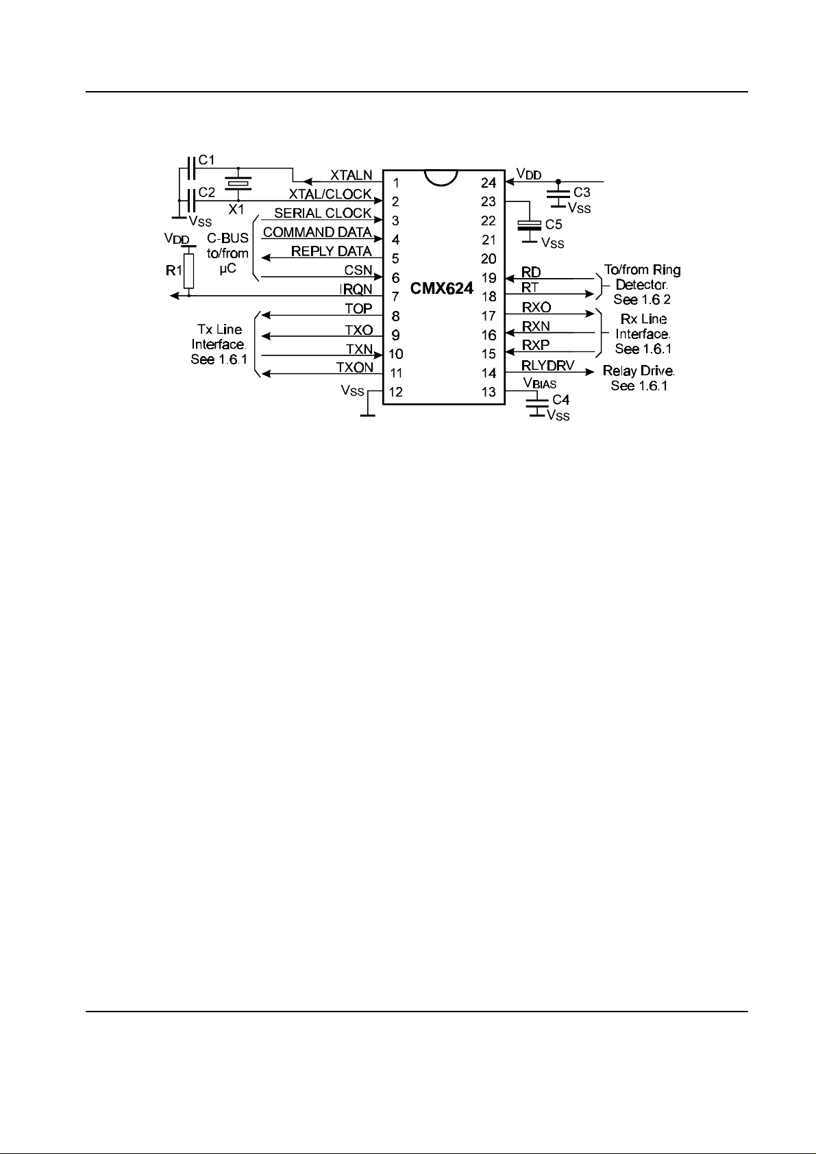
1.4 External Components
R1
100kΩ
X1 3.579545MHz
C1, C2 18pF
C3, C4
0.1µF
C5 *
Resistors
±5%, capacitors ±10% unless otherwise stated.
* This component is only required for compatibility with CMX644A,
see CMX644A Data Sheet for further details.
Figure 2 Recommended External Components for Typical Application
1.5 General Description
The CMX624 contains a V.23/Bell 202 compatible FSK modem capable of duplex operation at 1200/75 or
1200/150 bps over a 2-wire line or 1200/1200 bps over a 4-wire line, a flexible FSK data UART, a receive FSK
or Call Progress Tone energy detector, a 2100Hz detector, a DTMF generator, a Tx line driving buffer
amplifier, a telephone line Ringing Signal or Line Voltage Reversal detector and a 3.579545MHz Xtal
oscillator. These functions are all controlled over a ‘C-BUS’ serial
and receive FSK modem data.
1.5.1 Xtal Osc and Clock Dividers
Frequency and timing accuracy of the CMX624 is determined by a 3.579545MHz clock present at the
XTAL/CLOCK pin. This may be generated by the on-chip oscillator inverter using the external components
C1, C2 and X1 of Figure 2, or may be supplied from an external source to the XTAL/CLOCK input. If the clock
is supplied from an external source, C1, C2 and X1 should not be fitted.
The on-chip oscillator is turned off in the 'Zero-Power' mode.
If the clock is provided by an external source which is not always running, then the 'Zero-Power' mode must
be set when the clock is not available. Failure to observe this rule may cause a rise in the supply current
drawn by CMX624.
µC interface which also carries the transmit
2001 Consumer Microcircuits Limited 6 D/624/6
Page 7
V23 / Bell 202 Modem CMX624
Call Progress
1.5.2 Rx Input Amplifier
This amplifier, with suitable external components, is used to adjust the received signal to the correct amplitude
for the FSK receiver and Energy Detect circuits and may also form part of a 2-wire or 4-wire hybrid circuit; see
Section 1.6.1.
1.5.3 Receive Filter and Equaliser
This block includes a bandpass filter whose characteristics are set by bits 4 and 5 of the FSK MODE Register
according to the receive operating mode (Call Progress, 75/150bps FSK or 1200bps FSK). It is used to
attenuate out of band noise and interfering signals, especially the locally generated transmit FSK signal which
could otherwise interfere with the received FSK signal when the modem is operating in 2-wire duplex mode.
When receiving 1200bps FSK data an optional equaliser section, enabled by setting bit 6 of the FSK MODE
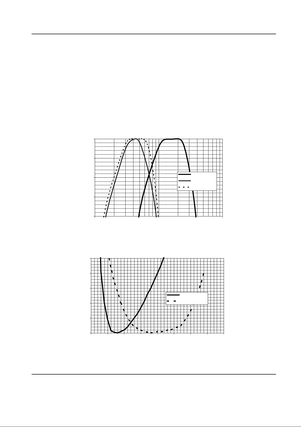
Register, compensates for one-half of the ETS Test Line 1 characteristics shown in Figure 3b.
0
-10
-20
dB
-30
-40
100 1000 10000
Hz
1200bps
75/150 bps
Figure 3a Rx Frequency Responses with Line Interface,
see section 1.6.1 (equaliser disabled)
5
4
3
dB
ms
2
1
dB wrt 800Hz
ms wrt 1700Hz
0
0 500 1000 1500 2000 2500 3000 3500 4000
Hz
Figure 3b ETS 300 114 Test Line 1 Characteristics (Normalised)
2001 Consumer Microcircuits Limited 7 D/624/6
Page 8
V23 / Bell 202 Modem CMX624
1.5.4 FSK Demodulator
This block is enabled when bits 1 and 5 of the FSK MODE Register are set to ‘1’, and converts the 75, 150 or
1200 bps FSK input signal to a binary received data signal which is sent to the Rx UART block.
Note that in the absence of a valid FSK signal, the demodulator may falsely interpret speech or other
extraneous signals as data.
1.5.5 Rx Energy and 2100Hz Detector
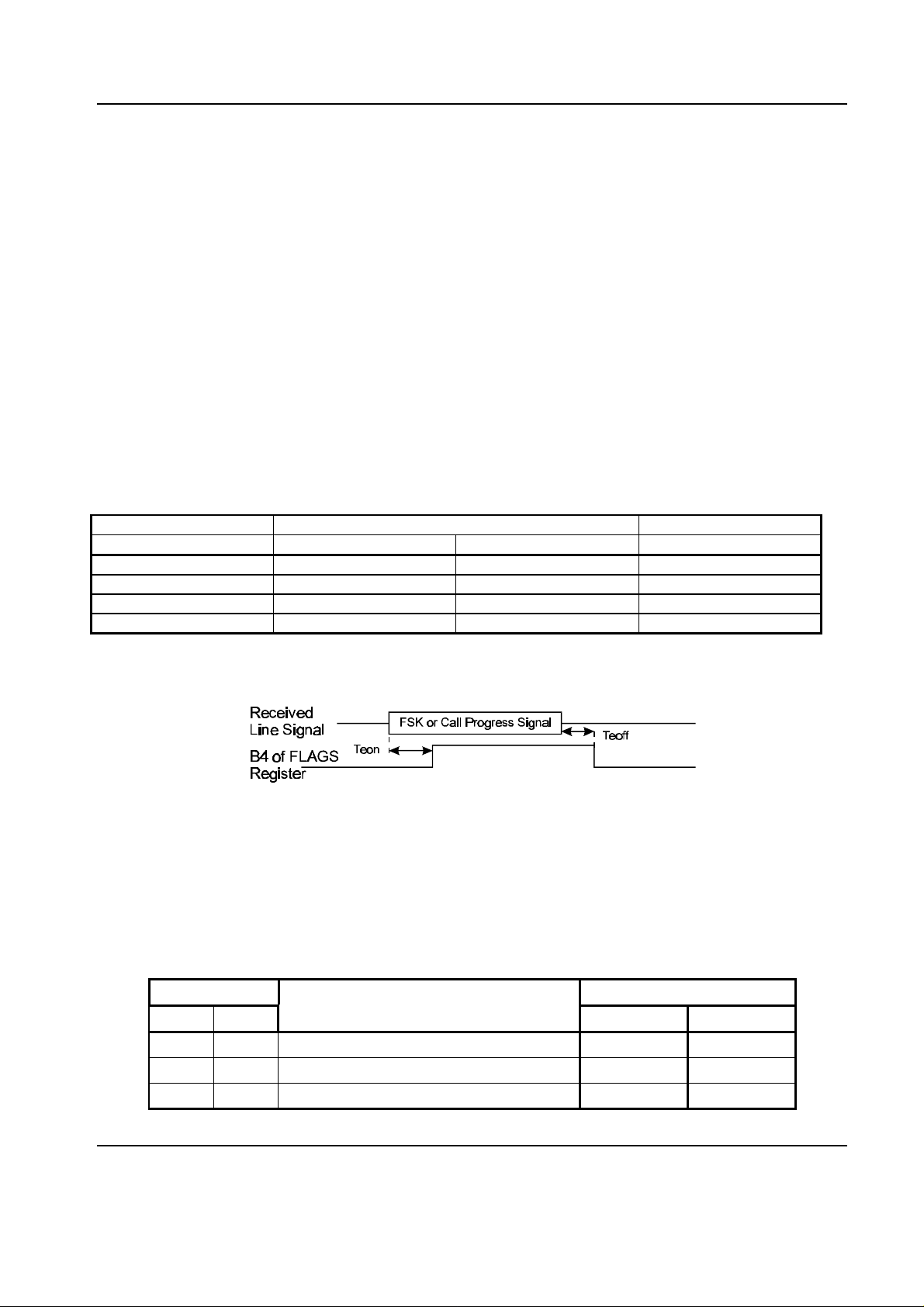
The function of this block is controlled by Bits 4 and 5 of the FSK MODE Register and Bit 0 of the TX TONES
Register.
When Bit 0 of the TX TONES Register and Bits 4 and 5 of the FSK MODE Register are set to ‘1’ this block will
measure the frequency and amplitude of the incoming signal. When a signal of 2100Hz is present of sufficient
amplitude and time Bit 4 of the FLAGS Register is set high. See Section 1.7.1 for amplitude, time and
frequency limits.
When Bit 0 of the TX TONES Register is set to ‘0’ this block compares the level of the signal at the output of
the Receive Filter against an internal threshold and may be used as a FSK level detector or a simple Call
Progress Signal detector according to the settings of bits 4 and 5 of the FSK MODE Register, which affect the
Receive Filter pass band as described in Section 1.5.3.
The required register settings are summarised in the table below:
TX TONES Reg
FSK MODE Reg
Bit 0 Bit 5 Bit 4 Detection Mode
0 0 0 Call Progress
0 1 0 75 / 150 bps FSK
0 1 1 1200 bps FSK
1 1 1 2100 Hz
Bit 4 of the FLAGS Register is set to ‘1’ by the output of this block when the received level has exceeded the
threshold for sufficient time. Amplitude and time hysteresis are used to reduce chattering in marginal
conditions.
See Section 1.7.1 for definitions of Teon and Teoff
1.5.6 FSK / DTMF Modulator
Figure 4 Rx Energy Detector Timing
When bit 7 of the TX TONES Register is set to ‘0’ then this block generates FSK signals as determined by
bits 0 and 1 of the FSK MODE Register and the Tx data bits from the UART block as shown in the tables
below:
V.23 mode (bit 7 of SETUP register = ‘0’):
FSK MODE Reg
FSK / DTMF Modulator block output FSK Signal Frequency
Bit 1 Bit 0 (Bit 7 of TX TONES = ‘0’) ‘0’ (Space) ‘1’ (Mark)
0 x Disabled (o/p held at VDD / 2) - 1 0 75bps FSK 450Hz 390Hz
1 1 1200bps FSK 2100Hz 1300Hz
2001 Consumer Microcircuits Limited 8 D/624/6
Page 9

V23 / Bell 202 Modem CMX624
Bell 202 mode (bit 7 of SETUP register = ‘1’):
FSK MODE Reg
FSK / DTMF Modulator block output FSK Signal Frequency
Bit 1 Bit 0 (Bit 7 of TX TONES = ‘0’) ‘0’ (Space) ‘1’ (Mark)
0 x Disabled (o/p held at VDD / 2) - 1 0 150bps FSK 487Hz 387Hz
1 1 1200bps FSK 2200Hz 1200Hz
When bit 7 of the TX TONES Register is set to ‘1’, the block generates DTMF tone pairs or single tones from
the DTMF range as shown in the table below. Bit 6 of the TX TONES Register is then used to enable or
disable the block’s output to the Tx filter.
TX DATA Register Bits
0 - 3
D3
D2
D1
D0
Lower
Frequency (Hz)
DTMF Tone Pairs
(TX TONES Register Bit 4 = ‘0’)
Upper
Frequency (Hz)
Keypad
Legend
Single Tone
(Bit 4 = ‘1’)
Single Tone
Frequency (Hz)
0 0 0 0 941 1633 D 1633
0 0 0 1 697 1209 1 1209
0 0 1 0 697 1336 2 1336
0 0 1 1 697 1477 3 1477
0 1 0 0 770 1209 4 1209
0 1 0 1 770 1336 5 1336
0 1 1 0 770 1477 6 1477
0 1 1 1 852 1209 7 1209
1 0 0 0 852 1336 8 852
1 0 0 1 852 1477 9 852
1 0 1 0 941 1336 0 941
1 0 1 1 941 1209 * 941
1 1 0 0 941 1477 # 941
1 1 0 1 697 1633 A 697
1 1 1 0 770 1633 B 770
1 1 1 1 852 1633 C 852
1.5.7 Transmit Filter
This stage attenuates out of band signals present at the output of the FSK/DTMF modulator and also includes
a programmable 3dB level switch, selected by bit 2 of the FSK MODE Register.
The nominal output levels at the TOP pin when V
= 5.0V are as shown below.
DD
FSK MODE
Register bit 2
FSK Signal DTMF Tone
(Low group)
DTMF Tone
(High group)
0 (low level) -6dB -5dB -3dB
1 (high level) -3dB -2dB 0dB
0dB = 775mVrms
These levels are proportional to V
, and the actual transmit signal levels present on the 2- or 4-wire line will
DD
depend on the external circuitry as described in Section 1.6.1. Using the external components recommended
in Section 1.6.1 for a nominal FSK transmit level of -9dBm, DTMF tone levels of -8dBm and -6dBm, then the
out of band energy sent to the line will be within the limits shown in Figure 5 for both FSK and DTMF signals.
2001 Consumer Microcircuits Limited 9 D/624/6
Page 10

V23 / Bell 202 Modem CMX624
0
-10
Bell 202
-20
-30
dBm
V23
-40
-50
-60
-70
10 100 1000 10000 100000
Hz
Figure 5 Maximum Out of Band Tx Line Energy Limits
1.5.8 Transmit Output Buffer
This buffer amplifier, connected to the TXN, TXO and TXON pins, is intended for use as a Tx line driver as
shown in Section 1.6.1. Two symmetrical outputs are provided for use with a balanced load to give sufficient
Tx line signal levels even at low V
. If this is not required the TXON output can be disabled.
DD
If the buffer is used as a balanced line driver, then bit 6 of the SETUP Register should be set to ‘1’ (TXON
output enabled). Setting bit 6 to ‘0’ disables the TXON output and the buffer draws less current from the
supply. When bit 6 is set to '0' the TXON pin should be left open circuit. N.B. The TXO output is unaffected by
this bit.
1.5.9 Ring Signal Detector
This block, which functions even in Zero Power mode, can be used to detect a telephone line Ring Signal or
Line Voltage Reversal and then generate a Interrupt Request signal to wake up the µC at the start of a call.
Suitable interface circuits are shown in Section 1.6.2.
The output of this block is the ‘Ring Detect’ line shown in Figure 1 which directly drives bit 6 of the FLAGS
Register. Any ‘0’ to ‘1’ or ‘1’ to ‘0’ change on this line will also set the ‘Ring Detect Change’ bit (5) of the
FLAGS Register.
If this block is not used, then the RD and RT pins should be connected to V
and the ‘Ring Detect Change’
SS
bit (5) of the IRQ MASK Register set to ‘0’.
2001 Consumer Microcircuits Limited 10 D/624/6
Page 11

V23 / Bell 202 Modem CMX624
1.5.10 Tx/Rx UART
This block connects the µC, via the ‘C-BUS’ interface, to the received data from the FSK Demodulator and to
the transmit data input to the FSK Modulator.
As part of this function, the block can be programmed to convert data to be transmitted from 7 or 8-bit bytes to
asynchronous data characters, adding Start and Stop bits and - optionally - a parity bit to the data before
passing it to the FSK Modulator. Similarly, in the receive direction it can extract data bits from asynchronous
characters coming from the FSK Demodulator, stripping off the Start and Stop bits and performing an optional
Parity check on the received data before passing the result over the ‘C-BUS’ to the µC. Bits 0-3 of the SETUP
Register control the number of Stop and Data bits and the Parity options for both receive and transmit
directions.
Data to be transmitted should be loaded by the µC into the TX DATA Register when the Tx Data Ready bit (bit
0) of the FLAGS Register goes high. It will then be treated by the Tx UART block in one of two ways,
depending on the setting of bit 3 of the FSK MODE Register:
If the bit is ‘0’ (‘Tx Sync’ mode) then the 8 bits from the TX DATA Register will be transmitted
sequentially at 75, 150 or 1200bps, LSB (D0) first.
If bit 3 of the FSK MODE Register is ‘1’ (‘Tx Async’) then bits will be transmitted as asynchronous data
characters at 75, 150 or 1200 bps according to the following format:
One Start bit (Space).
7 or 8 Data bits from the TX DATA Register (D0-D6 or D0-D7) as determined by bit 0 of the
SETUP Register. LSB (D0) transmitted first.
Optional Parity bit (even or odd parity) as determined by bits 1 and 2 of the SETUP Register.
One or Two Stop bits (Mark) as determined by bit 3 of the SETUP Register.
In both cases data will only be transmitted if bit 1 of the FSK MODE Register is set to ‘1’.
Failure to load the TX DATA Register with a new value when required will result in bit 1 (Tx Data Underflow) of
the FLAGS Register being set to ‘1’ and if the ‘Tx Async’ mode of operation had been selected then a
continuous Mark (‘1’) signal will then be transmitted until a new value is loaded into TX DATA, whereas in ‘Tx
Sync’ mode the byte already in the TX DATA Register will be re-transmitted.
Figure 6a Transmit UART Function (Async)
2001 Consumer Microcircuits Limited 11 D/624/6
Page 12

V23 / Bell 202 Modem CMX624
Received data from the FSK Demodulator goes into the receive part of the UART block, where it is handled in
one of two ways depending on the setting of bit 7 of the FSK MODE Register:
If the bit is ‘0’ (‘Rx Sync’ mode) then the receive part of the UART block will simply take 8 consecutive
bits from the Demodulator and transfer them to the RX DATA Register (the first bit going into the D0
position). Note that this mode is intended for detection of simple data patterns such as ‘1010…’ or
continuous Mark or Space signals, the CMX624’s receive data clock extraction circuits are not
adequate to support a true synchronous receive data mode of operation.
If bit 7 of the FSK MODE Register is ‘1’ (‘ Rx Async’) then the received data output of the FSK
Demodulator is treated as 75, 150 or 1200 bps asynchronous characters each comprising:
A Start bit (Space).
7 or 8 Data bits as determined by bit 0 of the SETUP Register. These bits will be placed into
the RX DATA Register with the first bit received going into the D0 position.
An optional Parity bit as determined by bits 1 and 2 of the SETUP Register. If Parity is
enabled (bit 2 of the SETUP Register = ‘1’) then bit 7 of the FLAGS Register will be set to ‘1’ if
the received parity is incorrect.
At least one Stop bit (Mark).
Bit 2 (Rx Data Ready) of the FLAGS Register will be set to ‘1’ every time a new received value is loaded into
the RX DATA Register. If the previous contents of the RX DATA Register had not been read out over the ‘CBUS’ before the new value is loaded from the UART then bit 3 (Rx Data Overflow) of the FLAGS Register will
also be set to ‘1’.
Figure 6b Receive UART Function (Async)
2001 Consumer Microcircuits Limited 12 D/624/6
Page 13

V23 / Bell 202 Modem CMX624
1.5.11 ‘C-BUS’ Interface
This block provides for the transfer of data and control or status information between the CMX624’s internal
registers and the µC over the ‘C-BUS’ serial bus. Each transaction, see Figure 7, consists of a single Register
Address byte sent from the µC which may be followed by a single data byte sent from the µC to be written into
one of the CMX624’s Write Only Registers, or a single byte of data read out from one of the CMX624’s Read
Only Registers, as illustrated in Figure 7.
Data sent from the µC on the Command Data line is clocked into the CMX624 on the rising edge of the Serial
Clock input. Reply Data sent from the CMX624 to the µC is valid when the Serial Clock is high. The interface
is compatible with the most common µC serial interfaces such as SCI, SPI and Microwire, and may also be
easily implemented with general purpose µC I/O pins controlled by a simple software routine. See Figure 10
for detailed ‘C-BUS’ timing requirements.
Figure 7 ‘C-BUS’ Transactions
2001 Consumer Microcircuits Limited 13 D/624/6
Page 14

V23 / Bell 202 Modem CMX624
1.5.12 ‘C-BUS’ Registers
Write Only ‘C-BUS’ Registers
Command Data Byte Bits
Addr Reg. 7 6 5 4 3 2 1 0
$01 RESET
$E0
$E1
$E3
$E7
$EE
SETUP
TONES
MODE
MASK
TX
TX
DATA
FSK
IRQ
N/A N/A N/A N/A N/A N/A N/A N/A
FSK mode:
0 = V.23
1 = Bell 202
Tx Mode:
0 = FSK.
1 = Tones.
D7
0 = Rx Sync
1 = Async
Reserved,
Set to 0
TXON o/p:
0 = Off
1 = On
Tone or FSK
o/p:
0 = Off.
1 = On.
D6
Rx Equal:
0 = Off
1 = On
Reserved,
Set to 0
Relay Drive:
0 = o/c
1 = Pull low
Reserved,
set to 0
D5
0 = Rx Call
Progress
1 = Rx FSK
Ring Detect
Change
0 = Zero
Power
1 = Normal
0 = DTMF
1 = Single
tone
D4
0 = Rx 75 /
150 bps
1 = 1200
Reserved,
Set to 0
Stop bits:
0 = 1 bit
1 = 2 bits
Reserved,
set to 0
D3
0 = Tx Sync
1 = Async
Rx Data
overflow
Parity:
0 = None
1 = Parity
Reserved,
set to 0
D2
Tx o/p level:
0 = Normal
1 = +3dB
Rx Data
ready
Parity:
0 = Odd
1 = Even
Reserved,
set to 0
D1
FSK enable:
0 = Off
1 = On
(Tx & Rx)
Tx Data
underflow
Data bits:
0 = 8 bits
1 = 7 bits
Set Detect:
0 = FSK/CP
1 = 2100Hz
D0
0 = Tx 75 /
150 bps
1 = 1200 or
DTMF
Tx Data
ready
Read Only ‘C-BUS’ Registers
Reply Data Byte Bits
Addr Reg. 7 6 5 4 3 2 1 0
RX
D7
Bad Rx
Parity
$EA
DATA
$EF
FLAGS
** See notes 2 and 3
D6
Ring Detect Ring Detect
D5
Change **
D4
Rx Energy
or 2100Hz
detect.
D3
Rx Data
overflow **
D2
Rx Data
ready **
D1
Tx Data
underflow **
D0
Tx Data
ready **
Notes:
1. Accessing the RESET Register over the ‘C-BUS’ clears all of the bits in the SETUP, TX TONES, TX
DATA, FSK MODE and IRQ MASK registers, and bits 0-3 and 5 of the FLAGS Register to ‘0’. This
will set the device into Zero Power mode. Note that this is a single-byte ‘C-BUS’ transaction
consisting solely of the address byte value $01.
Note that putting the device in Zero Power mode by directly setting SETUP Bit 4 to ‘0’ does not clear
the other register bits. Care should be taken before re-enabling the device that the other bits are set
so as to prevent undesired transient operation. In particular, bit 6 of the TXTONES Register should
be set to ‘0’ to prevent modulation of the transmitter output.
2. If any of bits 0, 1, 2, 3 or 5 of the FLAGS Register is ‘1’ and the corresponding bit of the IRQ MASK
Register is also ‘1’ then the IRQN output of the CMX624 will be pulled low.
3. Bit 5 (Ring Detect Change) of the FLAGS Register is set on every ‘0’ to ‘1’ or ‘1’ to ‘0’ change of bit 6
(Ring Detect).
4. Clearing bit 4 of the SETUP Register puts the CMX624 into the Zero Power mode by turning off all
blocks except for the ‘C-BUS’ interface and Ring Detector circuit.
5. Reading the FLAGS Register clears the IRQN output and also clears bits 0, 1, 2, 3 and 5 of the
FLAGS Register.
6. FLAGS Register (bit 4) is ‘1’ whenever the received signal being looked for is detected and ‘0’ when
both signals are absent. IRQ MASK Register (bit 4) is normally set to ‘0’ - but can be set to ‘1’ to
enable interrupts on the IRQN output. In the latter case, IRQN will be continuously pulled to ‘0’
whilst Rx Energy or 2100Hz are present. This may be useful for device evaluation purposes.
1.6 Application Notes
2001 Consumer Microcircuits Limited 14 D/624/6
Page 15

V23 / Bell 202 Modem CMX624
1.6.1 Line Interface
A line interface circuit is needed to provide dc isolation between the modem and the line, to perform line
impedance termination, and to set the correct transmit and receive signal levels.
4-Wire Line Interface
Figure 8a shows an interface circuit for use with a 600
and R15, while R11 and R13 should be selected to give the desired transmit and receive levels.
The gain of the receive input amplifier (R12 / R11) should be set to compensate for the loss of the input
transformer and the supply voltage.
Assuming transformer loss of about 1dB, R11 should be 91k
Ω 4-wire line. The line terminations are provided by R10
Ω at 5.0V, or 130kΩ at 3.0V.
Note relay circuit, ac and dc loads and line protection not shown for clarity.
R10
600Ω
R13 See text C10 100nF
R11 See text R14
R12
100kΩ
R15
100kΩ
600Ω
C11 220pF
C12 330pF
C13 100nF
Resistors
±1%, capacitors ±20%.
Figure 8a 4-Wire Line Interface Circuit
2001 Consumer Microcircuits Limited 15 D/624/6
Page 16

V23 / Bell 202 Modem CMX624
In the transmit direction, the level on the 4-wire line is determined by the level at the TOP pin, the gain
of the Output Buffer Amplifier, a loss of nominally 6dB due to the line termination resistor R15, and the loss in
the transformer.
The TOP pin signal level is proportional to V
and is also affected by the setting of the Tx o/p level control bit
DD
(bit 2) of the FSK Mode Register.
Assuming that the Tx o/p level control bit is set to ‘1’ (giving a FSK signal level of -3dB wrt 775mVrms at the
TOP pin when V
= 5.0V) and that there is 1dB loss in the transformer, then:
DD
Tx FSK 4-wire line level = -(3 +6 +1) + 20 x LOG
10(2 x R14 / R13) + 20 x LOG10(V
/ 5.0) dBm
DD
For example, to generate a nominal Tx FSK line level of -9dBm, R13 should be 180k
falling to 120k
Ω at 3.3V.
Ω when V
= 5.0V,
DD
2-Wire Line Interface
Figure 8b shows an interface circuit suitable for connection to a 600
Ω 2-wire line. The circuit also shows how
a relay may be driven from the RLYDRV pin. Note that when the CMX624 is powered from less than 5.0V,
buffer circuitry will be required to drive a 5V relay.
Note ac and dc loads and line protection not shown for clarity.
R11 See text R15
R12
100kΩ
R16
R13 See text R17
R14
100kΩ
Resistors
±1%, capacitors ±20%
600Ω
120kΩ
100kΩ
C11 220pF
C12 330pF
C13 10nF
C14 100nF
Figure 8b 2-Wire Line Interface Circuit
This circuit includes a 2-wire to 4-wire hybrid circuit, formed by R11, R15, R16, R17, C13 and the impedance
of the line itself, which ensures that the modem receive input and transmit output paths are both coupled
efficiently to the line, while minimising coupling from the modem’s transmit signal into the receive input.
The values of R11 and R13 should be calculated in the same way as for the 4-wire interface circuit of Figure
8a.
2001 Consumer Microcircuits Limited 16 D/624/6
Page 17

V23 / Bell 202 Modem CMX624
1.6.2 Ring Detector Interface
Figure 9 shows how the CMX624 may be used to detect the large amplitude Ringing signal received at the
start of an incoming telephone call.
The ring signal is usually applied at the subscriber's exchange as an ac voltage inserted in series with one of
the telephone wires and will pass through either C20 and R20 or C21 and R21 to appear at the top end of R22
(point X in Figure 9) in a rectified and attenuated form.
The signal at point X is further attenuated by the potential divider formed by R22 and R23 before being applied
to the CMX624 RD input. If the amplitude of the signal appearing at RD is greater than the input threshold
(Vthi) of Schmitt trigger 'A' then the N transistor connected to RT will be turned on, pulling the voltage at RT to
by discharging the external capacitor C22. The output of the Schmitt trigger 'B' will then go high, setting bit
V
SS
6 (Ring Detect) of the FLAGS Register.
The minimum amplitude ringing signal that is certain to be detected is:
( 0.7 + Vthi x [R20 + R22 + R23] / R23 ) x 0.707 Vrms
where Vthi is the high-going threshold voltage of the Schmitt trigger A (see Section 1.7.1).
With R20-22 all 470k
40Vrms and above for V
Ω as Figure 9, then setting R23 to 68kΩ will guarantee detection of ringing signals of
over the range 3.0 to 5.5V.
DD
2001 Consumer Microcircuits Limited 17 D/624/6
R20, 21, 22
470kΩ
C20, 21
R23 See text C22
R24
470kΩ
Resistors
±1%, capacitors ±20%
D1-4 1N4004
Figure 9 Ring Signal Detector Interface Circuit
0.1µF
0.33µF
Page 18

V23 / Bell 202 Modem CMX624
If the time constant of R24 and C22 is large enough then the voltage on RT will remain below the threshold of
the 'B' Schmitt trigger for the duration of a ring cycle.
The time for the voltage on RT to charge from V
towards VDD can be derived from the formula
SS
VRT = V
x [1 - exp(-t/(R24 x C22)) ]
DD
As the Schmitt trigger high-going input threshold voltage (Vthi) has a minimum value of 0.56 x V
Schmitt trigger B output will remain high for a time of at least 0.821 x R24 x C22 following a pulse at RD.
, then the
DD
The values of R24 and C22 given in Figure 9 (470k
Ω and 0.33µF) give a minimum RT charge time of 100
msec, which is adequate for ring frequencies of 10Hz or above.
Note that the circuit will also respond to a telephone line voltage reversal. If necessary the
µC can distinguish
between a Ring signal and a line voltage reversal by measuring the time that bit 6 of the FLAGS Register
(Ring Detect) is high.
2001 Consumer Microcircuits Limited 18 D/624/6
Page 19

V23 / Bell 202 Modem CMX624
1.7 Performance Specification
1.7.1 Electrical Performance
1.7.1.1 Absolute Maximum Ratings
Exceeding these maximum ratings can result in damage to the device.
Supply (VDD - VSS) -0.3 7.0 V
Voltage on any pin to V
Current into or out of VDD and V
-0.3 V
SS
pins -50 +50 mA
SS
Current into RLYDRV pin
Current into or out of any other pin -20 +20 mA
D2 Package
Min. Max. Unit
Total Allowable Power Dissipation at Tamb = 25°C
... Derating
Storage Temperature -55 +125 °C
Operating Temperature -40 +85 °C
D5 Package
Min. Max. Unit
Total Allowable Power Dissipation at Tamb = 25°C
... Derating
Storage Temperature -55 +125 °C
Operating Temperature -40 +85 °C
P4 Package
Min. Max. Unit
Total Allowable Power Dissipation at Tamb = 25°C
... Derating
Storage Temperature -55 +125 °C
Operating Temperature -40 +85 °C
1.7.1.2 Operating Limits
Correct operation of the device outside these limits is not implied.
Supply (VDD - VSS)
Operating Temperature
Notes Min. Max. Unit
Xtal Frequency 1 3.575965 3.583125 MHz
Notes: 1. A Xtal frequency of 3.579545MHz ±0.1% is required for correct operation.
Min. Max. Unit
+ 0.3 V
DD
+50 mA
800 mW
13 mW/°C
550 mW
9 mW/°C
800 mW
13 mW/°C
2.7 5.5 V
-40 +85 °C
2001 Consumer Microcircuits Limited 19 D/624/6
Page 20

V23 / Bell 202 Modem CMX624
1.7.1.3 Operating Characteristics
Details in this section represent design target values and are not currently guaranteed.
For the following conditions unless otherwise specified:
V
= 2.7V at Tamb = 25°C and V
DD
Xtal Frequency = 3.579545MHz
= 3.0V to 5.5V at Tamb = -40 to +85°C,
DD
± 0.1%, 0dBm corresponds to 775mVrms.
DC Parameters
IDD (Zero Power mode) 1, 2 - 1.0 -
Notes Min. Typ. Max. Unit
µA
(Running, TXON o/p Off, VDD= 5.0V) 1 - 3.4 6.0 mA
(Running, TXON o/p Off, V
(Running, TXON o/p On, V
(Running, TXON o/p On, V
Logic '1' Input Level
Logic '0' Input Level
3 70% - - V
3 - - 30% V
Logic Input Leakage Current (Vin = 0 to V
(excluding XTAL/CLOCK input)
Output Logic '1' Level (l
Output Logic '0' Level (l
OH
OL
IRQN O/P 'Off' State Current (Vout = V
Schmitt trigger input high-going threshold (Vthi)
(see Figure 11)
Schmitt trigger input low-going threshold (Vtlo)
(see Figure 11)
RLYDRV ‘ON’ resistance to VSS (VDD= 5.0V)
= 3.3V) 1 - 1.8 3.2 mA
DD
= 5.0V) 1 - 3.5 6.2 mA
DD
= 3.3V) 1 - 1.9 3.4 mA
DD
DD
),
-1.0 - +1.0
= 360µA)
= 360µA)
DD
)
VDD-0.4 - - V
- - 0.4 V
- - 1.0
0.56V
- 0.56V
DD
+ 0.6V
0.44V
DD
- 0.6V
- 38.0 TBD
- 0.44V
DD
V
DD
DD
DD
µA
µA
V
Ω
Notes: 1. At 25
°C, not including any current drawn from the CMX624 pins by external circuitry other
than X1, C1 and C2.
2. All logic inputs at V
except for RT and CSN inputs which are at VDD.
SS
3. Excluding RD, RT and XTAL/CLOCK pins.
FSK Modulator and Tx UART
Notes Min. Typ. Max. Unit
Level at TOP pin. 4 -4.0 -3.0 -2.0 dBm
Twist (Mark level WRT Space level)
Tx 1200bits/sec (V.23 mode)
Baud Rate (set by UART and Xtal frequency)
Mark (Logical 1) Frequency
Space (Logical 0) Frequency
Tx 75bits/sec (V.23 mode)
Baud Rate (set by UART and Xtal frequency)
Mark (Logical 1) Frequency
Space (Logical 0) Frequency
Tx 1200bits/sec (Bell 202 mode)
Baud Rate (set by UART and Xtal frequency)
Mark (Logical 1) Frequency
Space (Logical 0) Frequency
Tx 150bits/sec (Bell 202 mode)
Baud Rate (set by UART and Xtal frequency)
Mark (Logical 1) Frequency
Space (Logical 0) Frequency
-2.0 0 +2.0 dB
1194 1200 1206 Baud
1297 1300 1303 Hz
2097 2100 2103 Hz
74 75 76 Baud
388 390 392 Hz
448 450 452 Hz
1194 1200 1206 Baud
1197 1200 1203 Hz
2197 2200 2203 Hz
149 150 151 Baud
385 387 389 Hz
485 487 489 Hz
Notes: 4. At V
= 5.0V, Tx o/p level control bit set to ‘1’; load resistance greater than 40kΩ.
DD
2001 Consumer Microcircuits Limited 20 D/624/6
Page 21

V23 / Bell 202 Modem CMX624
DTMF Transmitter
Notes Min. Typ. Max. Unit
Level at TOP pin; tones in High Group 4 -1.0 0.0 +1.0 dBm
Twist (level of High Group tones WRT level of
Low Group tones)
Tone frequency accuracy (worst case)
- +2.0 - dB
-0.5 - +0.5 %
Tx Filter and Output Buffer
Change in level at TOP pin caused by changing
bit 2 of FSK MODE Register
Buffer output signal swing;
Load greater than 500
Notes Min. Typ. Max. Unit
2.5 3.0 3.5 dB
5 2.2 - - Vp-p
Ω.
Notes: 5. For each of the TXON (if enabled) and TXO pins, load between pin and V
DD
/ 2.
FSK Demodulator and Rx UART
Notes Min. Typ. Max. Unit
Valid Input Level Range 6 -43.0 - -9.0 dBm
Acceptable Twist (Mark level WRT Space level)
-7.0 - +7.0 dB
Acceptable Signal to Noise Ratio 7 20.0 - - dB
Rx 1200bits/sec (V.23 mode)
Acceptable Rx Data Rate 8 1188 1200 1212 Baud
Mark (Logical 1) Frequency
Space (Logical 0) Frequency
Rx 75bits/sec (V.23 mode)
1280 1300 1320 Hz
2068 2100 2132 Hz
Acceptable Rx Data Rate 8 TBD 75 TBD Baud
Mark (Logical 1) Frequency
Space (Logical 0) Frequency
Rx 1200bits/sec (Bell 202 mode)
TBD 390 TBD Hz
TBD 450 TBD Hz
Acceptable Rx Data Rate 8 1188 1200 1212 Baud
Mark (Logical 1) Frequency
Space (Logical 0) Frequency
Rx 150bits/sec (Bell 202 mode)
1180 1200 1220 Hz
2168 2200 2232 Hz
Acceptable Rx Data Rate 8 TBD 150 TBD Baud
Mark (Logical 1) Frequency
Space (Logical 0) Frequency
TBD 387 TBD Hz
TBD 487 TBD Hz
Notes: 6. Measured at point A in Figures 8a and 8b, for V
proportional to V
. To cater for other supply voltages or different signal level ranges the
DD
= 5.0V. The internal threshold levels are
DD
voltage gain of the Rx Input Amplifier should be adjusted by selecting the appropriate external
components as described in Section 1.6.1.
7. Flat noise in 300-3400 Hz band for V.23, 200-3400 Hz for Bell 202.
8. Set by Rx UART and Xtal frequency.
2100Hz Detector
‘Will Decode’ Frequency Range
‘Will Not Decode’ Frequency Range
Notes Min. Typ. Max. Unit
2040 - 2235 Hz
<2010 - >2265 Hz
‘Off’ to ‘On’ time 9 - - 25 ms
‘On’ to ‘Off’ time 9 4.0 - - ms
Notes: 9. 2100Hz detection requires a signal within the amplitude range given in the Rx Energy
Detector section.
2001 Consumer Microcircuits Limited 21 D/624/6
Page 22

V23 / Bell 202 Modem CMX624
Rx Energy Detector
Notes Min. Typ. Max. Unit
‘Off’ to 'On' Threshold Level (FSK) 6, 10 -48.0 - -43.0 dBm
‘Off’ to 'On' Threshold Level (Call Progress) 6, 10 -48.0 - -40.0 dBm
Hysteresis (measured at V
DD = 3V and 5V)
'Off' to 'On' Time (Figure 4 Teon): 6, 10
1200bps Rx mode
75/150bps Rx mode
Call Progress Detect mode
'On' to 'Off' Time (Figure 4 Teoff): 6, 10
1200bps Rx mode
75/150bps Rx mode
Call Progress Detect mode
6, 10 2.0 - - dB
- - 25 ms
- - 48 ms
- - 48 ms
8.0 - - ms
20 - - ms
20 - - ms
Notes: 10. Measured with 1300Hz signal in 1200bps mode, 390Hz for 75 or 150 bps and Call Progress
mode, signal level -33dBm for time delay measurements.
XTAL/CLOCK Input
Notes Min. Typ. Max. Unit
'High' Pulse Width 11 100 - - ns
'Low' Pulse Width 11 100 - - ns
Notes: 11. Timing for an external input to the XTAL/CLOCK pin.
‘C-BUS’ Timings (See Figure 10)
t
CSN-Enable to Clock-High time
CSE
t
Last Clock-High to CSN-High time
CSH
t
Clock-Low to Reply Output enable
LOZ
t
CSN-High to Reply Output 3-state time
HIZ
t
t
t
t
t
t
t
t
t
CSN-High Time between transactions
CSOFF
Inter-Byte Time
NXT
Clock-Cycle time
CK
Serial Clock-High time
CH
Serial Clock-Low time
CL
Command Data Set-Up time
CDS
Command Data Hold time
CDH
Reply Data Set-Up time
RDS
Reply Data Hold time
RDH
time
Notes Min. Typ. Max. Unit
100 - - ns
100 - - ns
0.0 - - ns
- - 1.0 µs
1.0 - - µs
200 - - ns
200 - - ns
100 - - ns
100 - - ns
75 - - ns
25 - - ns
50 - - ns
0 - - ns
Note: These timings are for the latest version of the ‘C-BUS’ as embodied in the CMX624, and allow faster
transfers than the original ‘C-BUS’ timings given in CML Publication D/800/Sys/3 July 1994.
2001 Consumer Microcircuits Limited 22 D/624/6
Page 23

V23 / Bell 202 Modem CMX624
Figure 10 ‘C-BUS’ Timing
3.5
3
2.5
2
Vin
1.5
1
0.5
0
2.5 3 3.5 4 4.5 5 5.5
Vdd
Vthi
Vtlo
Figure 11 Typical Schmitt Trigger Input Voltage Thresholds vs. V
DD
2001 Consumer Microcircuits Limited 23 D/624/6
Page 24

V23 / Bell 202 Modem CMX624
1.7.2 Packaging
Figure 12a 24-pin SOIC (D2) Mechanical Outline: Order as part no. CMX624D2
Figure 12b 24-pin SSOP (D5) Mechanical Outline: Order as part no. CMX624D5
2001 Consumer Microcircuits Limited 24 D/624/6
Page 25

V23 / Bell 202 Modem CMX624
Figure 12c 24-pin DIL (P4) Mechanical Outline: Order as part no. CMX624P4
Handling precautions: This product includes input protection, however, precautions should be taken to prevent device damage from
electro-static discharge. CML does not assume any responsibility for the use of any circuitry described. No IPR or circuit patent
licences are implied. CML reserves the right at any time without notice to change the said circuitry and this product specification.
CML has a policy of testing every product shipped using calibrated test equipment to ensure compliance with this product
specification. Specific testing of all circuit parameters is not necessarily performed.
Oval Park - LANGFORD
MALDON - ESSEX
CM9 6WG - ENGLAND
Telephone: +44 (0)1621 875500
Telefax: +44 (0)1621 875600
e-mail: sales@cmlmicro.co.uk
http://www.cmlmicro.co.uk
 Loading...