

Page 1

DATA BULLETIN
Bell 202 and V.23 Modem
CMX624
with Call Progress and DTMF
PRELIMINARY INFORMATION
Features Applications
•
Bell 202 and V.23 Compatible Modem
•
1200bps Full duplex Operation (2 or 4 Wire)
•
Software Adjustable Tx and Rx Levels
•
Programmable Group Delay Equalizer
•
Answer/Originate Tone Generator/Detector
•
Call Progress Tone Detection
•
Integrated DTMF Encoder
•
Line Reversal and Ring Detector
•
Simple Serial Control Interface
•
Hook Switch Relay Driver
•
Zero-Power Standby Mode
•
3.0 to 5.0V Operation
Ring & Line
Reversal Detect
Transmit
Filter
µC
IRQ
CS
CLK
RXD
TXD
Serial
Interface
+
Tx/Rx Data
UART
Call Progress
and
Data Detect
FSK
De-modulator
FSK/DTMF
Modulator
Receive
Filter and
Equalizer
V
•
•
•
•
•
•
•
•
Xtal Osc and
Clock Dividers
BIAS
Telephone Telemetry Systems
Remote Utility Meter Reading
Security Systems
Payphones
Cable-TV Set Top Boxes
Industrial Control Systems
Electronic Cash Terminals
Vending Machines
RT
RD
XTAL/CLK
XTAL
RXRX+
RXAMPOUT
TXINTX+
TXTX
RLYDRV
Passive
Hybrid
Network
2 or 4
Wire Line
The CMX624 Bell 202 and V.23 modem provides full duplex 1200bps data signaling suitable for telephone
based information and telemetry systems where low power operation is desired. Bell 202 and V.23 signaling
delivers fast call set up times and robust, error resistant, transmission in 2 or 4 wire line circuits. A rich set of
important additional functions enhances end product value while reducing size. These include: integrated
DTMF encoder for dial out functions, single tone encoder for ‘melody’ generation, answer tone
generator/detector, line reversal and ring detector for ‘waking’ up a sleeping µC, adjustable Tx and Rx gain,
and a low impedance pull down output for hook relay control. The addition of the answer tone
generator/detector and call progress tone detector makes the set-up of a telephone call much easier for the
host µC to accomplish.
Very low power telemetry and data collection applications are supported by the CMX624’s ‘Zero Power’
standby mode in which the device will detect telephone line ringing voltage or line voltage reversal events.
Pin compatible with the CMX644A Bell212A / V.22 modem, the CMX624 is available in the following
packages: 24-pin SSOP (CMX624D5), 24-pin SOIC (CMX624D2), and 24-pin PDIP (CMX624P4).
1999 MX-COM, Inc. www.mxcom.com Tel: 800 638 5577 336 744 5050 Fax: 336 744 5054 Doc. # 20480180.108
4800 Bethania Station Road, Winston-Salem, NC 27105-1201 USA All trademarks and service marks are held by their respective companies.
Page 2

Bell 202 and V.23 Compatible Modem 2 CMX624 Preliminary Information
CONTENTS
Section Page
1 Block Diagram................................................................................................................3
2 Signal List.......................................................................................................................4
3 External Components....................................................................................................5
4 General Description.......................................................................................................6
4.1 ‘C-BUS’ Serial Interface....................................................................................................... 6
4.2 Software Description ........................................................................................................... 7
4.3 Xtal Oscillator ...................................................................................................................... 8
4.4 Rx Input Amplifier ................................................................................................................ 8
4.5 Receive Filter....................................................................................................................... 8
4.6 Equalizer.............................................................................................................................. 8
4.7 FSK Demodulator................................................................................................................ 9
4.8 Rx Energy and 2100Hz Detector....................................................................................... 10
4.9 FSK / DTMF Modulator...................................................................................................... 10
4.9.1 V.23 mode (Bit 7 of SETUP register = ‘0’):...........................................................................10
4.9.2 Bell 202 mode (Bit 7 of SETUP register = ‘1’):.....................................................................11
4.10 Transmit Filter.................................................................................................................... 12
4.11 Transmit Output Buffer......................................................................................................12
4.12 Ring Signal Detector.......................................................................................................... 12
4.13 Tx/Rx UART ...................................................................................................................... 13
5 Application Notes ........................................................................................................15
5.1 Line Interface..................................................................................................................... 15
5.1.1 4-Wire Line Interface............................................................................................................15
5.1.2 2-Wire Line Interface............................................................................................................16
5.2 Ring Detector Interface......................................................................................................17
6 Performance Specification..........................................................................................19
6.1 Electrical Performance ...................................................................................................... 19
6.1.1 Absolute Maximum Ratings.................................................................................................. 19
6.1.2 Operating Limits...................................................................................................................19
6.1.3 Operating Characteristics.....................................................................................................20
6.1.4 Timing...................................................................................................................................24
6.2 Packaging.......................................................................................................................... 25
MX-COM, Inc. reserves the right to change specifications at any time and without notice.
1999 MX-COM, Inc. www.mxcom.com Tel: 800 638 5577 336 744 5050 Fax: 336 744 5054 Doc. # 20480180.108
4800 Bethania Station Road, Winston-Salem, NC 27105-1201 USA All trademarks and service marks are held by their respective companies.
Page 3
Bell 202 and V.23 Compatible Modem 3 CMX624 Preliminary Information
1 Block Diagram
RT
µC
IRQ
CS
CLK
RXD
TXD
Serial
Interface
+
Tx/Rx Data
UART
Call Progres s
Data Detect
De-modulator
FSK/DTMF
Modulator
Ring & Line
Reversal Detect
and
FSK
Transmit
Receive
Filter and
Equalizer
Filter
Figure 1: Block Diagram
Xtal Osc and
Clock Dividers
V
BIAS
RD
XTAL/CLK
XTAL
RXRX+
RXAMPOUT
TXINTX+
TX-
TX
RLYDRV
Passive
Hybrid
Network
2 or 4
Wire Line
1999 MX-COM, Inc. www.mxcom.com Tel: 800 638 5577 336 744 5050 Fax: 336 744 5054 Doc. # 20480180.108
4800 Bethania Station Road, Winston-Salem, NC 27105-1201 USA All trademarks and service marks are held by their respective companies.
Page 4
Bell 202 and V.23 Compatible Modem 4 CMX624 Preliminary Information
2 Signal List
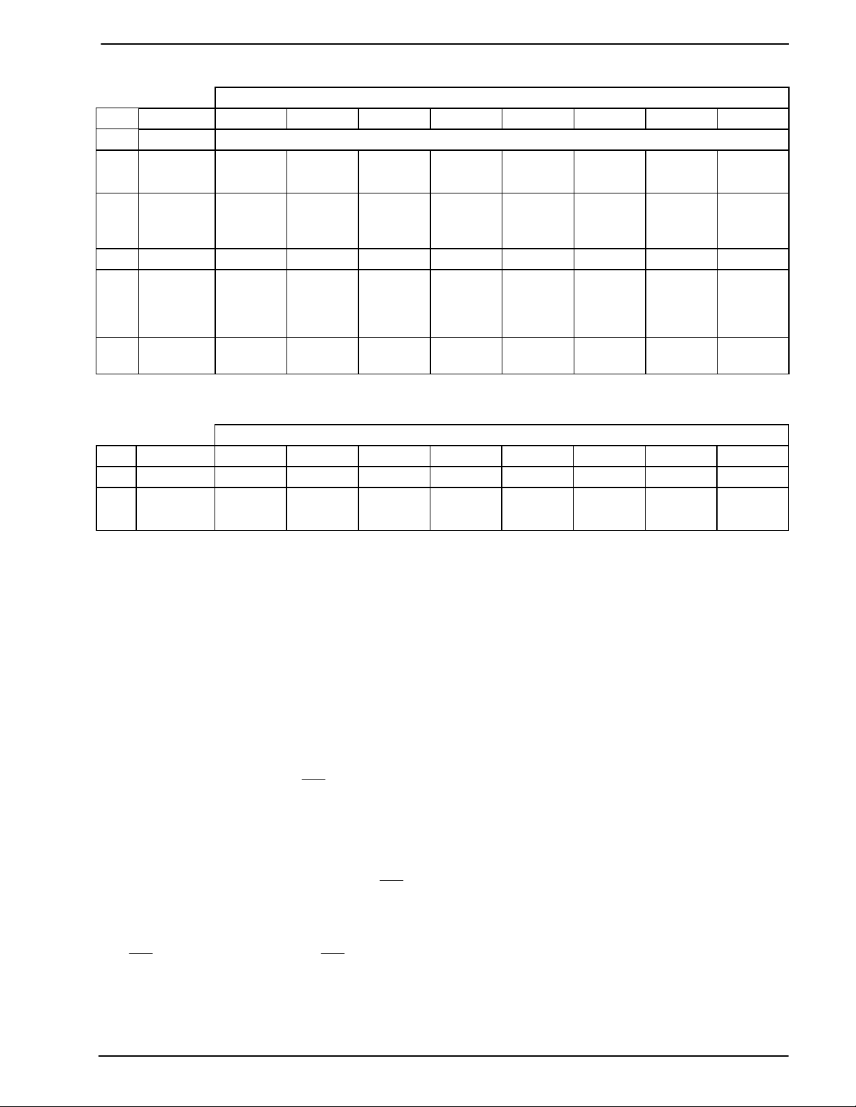
Pin No. Name Type Description
1
XTAL
2 XTAL/CLOCK input
3
SERIAL
CLOCK
4 COMMAND
DATA
5REPLY
DATA
6
7
CS
IRQ
8 TX output The Tx analog signal output.
9 TX+ output The output of the line driving amplifier.
10 TXIN- input The inverting input to the line driver amplifier.
11 TX- output The inverted output of the line driving amplifier.
12 V
13 V
SS
BIAS
14 RLYDRV output
15 RX+ input The non-inverting input to the Rx input amplifier.
16 RX- input The inverting input to the Rx input amplifier.
17 RXAMPOUT output The output of the Rx input amplifier.
18 RT bi-directional
19 RD input Schmitt trigger input to the Ring Signal Detector.
20 NC No connection should be made to this pin.
21 NC No connection should be made to this pin.
22 NC No connection should be made to this pin if the printed circuit
23 input No connection should be made to this pin if the printed circuit
24 V
DD
output The output of the on-chip Xtal oscillator inverter.
The input to the oscillator inverter from the Xtal circuit or
external clock source.
input
input
tri-state
The serial interface clock input from the µC. See Section 4.1
The serial interface data input from the µC.
A 3-state serial interface data output to the µC. This output is
high impedance when not sending data to the µC.
input
output
The serial interface transfer control input provided by the µC.
A ‘wire-ORable’ output for connection to a µC Interrupt Request
input. This output is pulled down to V
when active and is high
SS
impedance when inactive. An external pull-up resistor is
required.
Power The negative supply rail (ground).
output
Internally generated bias voltage of V
device is in ‘Zero Power’ mode when V
V
. Should be bypassed to VSS by a capacitor mounted close
SS
/2, except when the
DD
will discharge to
BIAS
to the device pins.
Relay drive open drain output. This output is pulled down to
V
when active and is high impedance when inactive.
SS
This pin is Bi-directional. An open drain output and Schmitt
trigger input forming part of the Ring Signal detector.
board is to be used for the CMX624 only. If the board is to be
used for the CMX644A, a capacitor should be connected as
shown in Figure 2.
board is to be used for the CMX624 only. If the board is to be
used for the CMX644A, a capacitor should be connected as
shown in Figure 2.
Power The positive supply rail. Levels and thresholds within the device
are proportional to this voltage. Should be bypassed to V
SS
by
a capacitor mounted close to the device pins.
Note: This device is capable of detecting and decoding small amplitude signals. To achieve this V
V
should be bypassed. It is very important to protect the receive path from extraneous in-band
BIAS
DD
and
signals. It is recommended that the printed circuit board be laid out with a ground plane in the
CMX624 area to provide a low impedance connection between the V
pin and the VDD and V
SS
BIAS
bypass capacitors.
1999 MX-COM, Inc. www.mxcom.com Tel: 800 638 5577 336 744 5050 Fax: 336 744 5054 Doc. # 20480180.108
4800 Bethania Station Road, Winston-Salem, NC 27105-1201 USA All trademarks and service marks are held by their respective companies.
Page 5
Bell 202 and V.23 Compatible Modem 5 CMX624 Preliminary Information
3 External Components
C1
V
DD
C5
RD
RT
RXAMPOUT
RX-
RX+
RLYDRV
V
BIAS
C4
C3
To/fro m Ring
Detector.
See 5.2
Rx Line
Interface.
See 5.1
Relay Drive.
See 5.1
V
DD
R1
C2
C-BUS
to/from
µC
Tx Line
Interface.
See 5.1
X1
XTAL/CLOCK
SERIAL CLOCK
COMMAND DATA
REPLY DATA
XTAL
CS
IRQ
TX
TX+
TXIN-
TX-
V
SS
1
2
3
4
5
6
CMX624
7
D5/D2/P4
8
9
10
11
12
24
23
22
21
20
19
18
17
16
15
14
13
Figure 2: Recommended External Components
R1
C1, C2 18pF
C3, C4
C5 Note 1
X1 Note 2 3.579545MHz
Tolerances for Resistors and Capacitors are as indicated unless otherwise stated.
Table 1: Recommended External Components
Notes:
1. This component is only required for compatibility with CMX644A, see CMX644A Data Bulletin for
additional details.
2. For best results, a crystal oscillator design should drive the clock inverter input with signal levels of at
least 40% of V
crystal oscillator design assistance, please consult you crystal manufacturer.
, peak to peak. Tuning fork crystals generally cannot meet this requirement. To obtain
DD
Ω±
100k
0.1µF
±
10%
±
10%
5%,
1999 MX-COM, Inc. www.mxcom.com Tel: 800 638 5577 336 744 5050 Fax: 336 744 5054 Doc. # 20480180.108
4800 Bethania Station Road, Winston-Salem, NC 27105-1201 USA All trademarks and service marks are held by their respective companies.
Page 6
Bell 202 and V.23 Compatible Modem 6 CMX624 Preliminary Information
4 General Description
The CMX624 contains a Bell 202 and V.23 compatible FSK modem. This device is capable of duplex
operation at 1200/75bps or 1200/150bps over a 2-wire line interface. It is also capable of 1200/1200bps over
a 4-wire line interface. This device also contains a flexible FSK data UART, a receive FSK or Call Progress
Tone energy detector, a 2100Hz detector, a DTMF generator, a Tx line driving buffer amplifier, a telephone
line Ringing Signal or Line Voltage Reversal detector and a 3.579545MHz Xtal oscillator. These functions are
controlled via a serial interface to the µC, which also carries the transmit and receive FSK modem data.
4.1 ‘C-BUS’ Serial Interface
This block provides for the transfer of data and control or status information between the CMX624’s internal
registers and the µC over the serial interface bus. Each ‘C-BUS’ transaction consists of a single Register
Address byte sent from the µC, as illustrated in Figure 3, which may be followed by either of:
1. A single data byte sent from the µC to be written into one of the CMX624’s Write Only Registers, as
illustrated in Figure 4.
2. A single byte of data read out from one of the CMX624’s Read Only Registers, as illustrated in Figure 5.
Data sent from the µC on the Command Data line is clocked into the CMX624 on the rising edge of the Serial
Clock input. Reply Data sent from the CMX624 to the µC is valid when the Serial Clock is high. The interface
is compatible with the most common µC serial interfaces such as SCI, SPI and Microwire, and may also be
easily implemented with general purpose µC I/O pins controlled by a simple software routine. See Figure 16
for detailed Serial Bus timing requirements.
CS
SERIAL CLOCK
COMMAND DATA
REPLY DATA
654
7
Address (01 Hex = Reset)
Hi-Z
321
0
Note:
The SERIAL CLOCK
line may be high or low at
the start and end of each
transaction.
= Level not important
Figure 3: Serial Bus Transaction (Single byte from µC)
CS
SERIAL CLOCK
COMMAND DATA
REPLY DATA
Hi-Z
654
7
Address
321
0
654
7
Data to CMX 6 2 4
321
0
Figure 4: Serial Bus Transactions (One Address and one Data byte from µC)
CS
SERIAL CLOCK
COMMAND DATA
REPLY DATA
Hi-Z
654
7
Address
321
0
654
7
Data from CMX624
321
0
Figure 5: Serial Bus Transactions (One Address byte from µC and one Reply byte from CMX624A)
1999 MX-COM, Inc. www.mxcom.com Tel: 800 638 5577 336 744 5050 Fax: 336 744 5054 Doc. # 20480180.108
4800 Bethania Station Road, Winston-Salem, NC 27105-1201 USA All trademarks and service marks are held by their respective companies.
Page 7
Bell 202 and V.23 Compatible Modem 7 CMX624 Preliminary Information
4.2 Software Description
Command Data Byte Bits
AddrReg.76543210
$01 RESET
$E0 SETUP
$E1 TX
TONES
$E3 TX DATA
$E7 FSK
MODE
$EE
IRQ
MASK
FSK mode:
0 = V.23
1 = Bell 202
Tx Mode:
0 = FSK.
1 = Tones.
D7 D6 D5 D4 D3 D2 D1 D0
0 = Rx Sync
1 = Async
Reserved,
Set to 0
TX- output:
0 = Off
1 = On
Tone or
FSK output:
0 = Off.
1 = On.
Rx Equal:
0 = Off
1 = On
Reserved,
Set to 0
Relay Drive:
0 = o/c
1 = Pull low
Reserved,
set to 0
0 = Rx Call
Progress
1 = Rx FSK
Ring Detect
Change
Table 2: Write Only Serial Bus Register
AddrReg.76543210
$EA RX DATA
$EF FLAGS
** See note 2 and 3
D7 D6 D5 D4 D3 D2 D1 D0
Bad Rx
Parity
Ring Detect
Ring Detect
Change **
SINGLE BYTE COMMAND
0 = Zero
Power
1 = Normal
0 = DTMF
1 = Single
tone
0 = Rx 75 /
150bps
1 = RX1200
Reserved,
Set to 0
Stop bits:
0 = 1 bit
1 = 2 bits
Reserved,
set to 0
0 = Tx Sync
1 = Async
Rx Data
overflow
Reply Data Byte Bits
Rx Energy
or 2100Hz
detect.
Rx Data
overflow **
Parity:
0 = None
1 = Parity
Reserved,
set to 0
Tx output
level:
0 = Normal
1 = +3dB
Rx Data
ready
Rx Data
ready **
Parity:
0 = Odd
1 = Even
Reserved,
set to 0
FSK
Enable:
0 = Off
1 = On
(Tx & Rx)
Tx Data
underflow
Tx Data
underflow **
Data bits:
0 = 8 bits
1 = 7 bits
Set Detect:
0 = FSK/CP
1 = 2100Hz
0 = Tx 75 /
150bps
1 = 1200 or
DTMF
Tx Data
ready
Tx Data
ready **
Table 3: Read Only Serial Bus Registers
Notes:
1. Accessing the RESET Register over the Serial Bus clears all of the bits in the SETUP, TX TONES, TX
DATA, FSK MODE and IRQ MASK registers, and Bits 0-3 and Bit 5 of the FLAGS Register to ‘0’. This
will set the device into Zero Power mode.
a) This is a single-byte Serial Bus transaction consisting solely of the address byte value $01.
b) Placing the device in Zero Power mode by directly setting SETUP Bit 4 to ‘0’ does not clear the other
register bits. Care should be taken before re-enabling the device that the other bits are set so as to
prevent undesired transient operation. In particular, bit 6 of the TXTONES Register should be set to
‘0’ to prevent modulation of the transmitter output.
2. If any of Bits 0, 1, 2, 3 or 5 of the FLAGS Register is ‘1’ and the corresponding bit of the IRQ MASK
Register is also ‘1’ then the
output of the CMX624 will be pulled low.
IRQ
3. Bit 5 (Ring Detect Change) of the FLAGS Register is set on every ‘0’ to ‘1’ or ‘1’ to ‘0’ change of Bit 6
(Ring Detect).
4. Clearing Bit 4 of the SETUP Register puts the CMX624 into the Zero Power mode by turning off all blocks
except for the Serial Bus interface and Ring Detector circuit.
5. Reading the FLAGS Register clears the
output and also clears Bits 0, 1, 2, 3 and 5 of the FLAGS
IRQ
Register.
6. FLAGS Register (bit 4) is ‘1’ whenever Rx Energy or 2100Hz are present and ‘0’ when both signals are
absent. IRQ Mask Register (bit 40 is normally set to ‘0’, but can be set to ‘1’ to enable interrupts on the
output. In the latter case,
IRQ
will be continuously pulled to ’0’ while Rx Energy or 2100Hz are
IRQ
present. This may be useful for device evaluation purposes.
1999 MX-COM, Inc. www.mxcom.com Tel: 800 638 5577 336 744 5050 Fax: 336 744 5054 Doc. # 20480180.108
4800 Bethania Station Road, Winston-Salem, NC 27105-1201 USA All trademarks and service marks are held by their respective companies.
Page 8
Bell 202 and V.23 Compatible Modem 8 CMX624 Preliminary Information
4.3 Xtal Oscillator
The frequency and timing accuracy of the CMX624 is determined by a 3.579545MHz clock signal input to the
XTAL/CLOCK pin. This may be generated by the on-chip oscillator inverter using the external components
C1, C2 and X1 or may be supplied from an external source to the XTAL/CLOCK input. See Figure 2. If the
clock is supplied from an external source, components C1, C2, and X1 should not be fitted.
The on-chip oscillator is disabled in the 'Zero-Power' mode.
If the clock is provided by an external source, which may not always be running, then the 'Zero-Power' mode
must be enabled when the clock is not available. Failure to observe this rule may cause an increase in the
supply current consumption by the CMX624.
4.4 Rx Input Amplifier
The Rx Input Amplifier, with suitable external components, is used to adjust the received signal to the correct
amplitude for the FSK receiver and Energy Detect circuits and may also form part of a 2-wire or 4-wire hybrid
circuit. See Section 5.1.
4.5 Receive Filter
This block includes a bandpass filter whose characteristics are set by Bits 4 and 5 of the FSK MODE Register
according to the receive operating mode (Call Progress, 75/150bps FSK or 1200bps FSK). It is used to
attenuate out of band noise and interfering signals; especially the locally generated transmit FSK signal that
could otherwise interfere with the received FSK signal when the modem is operating in 2-wire duplex mode.
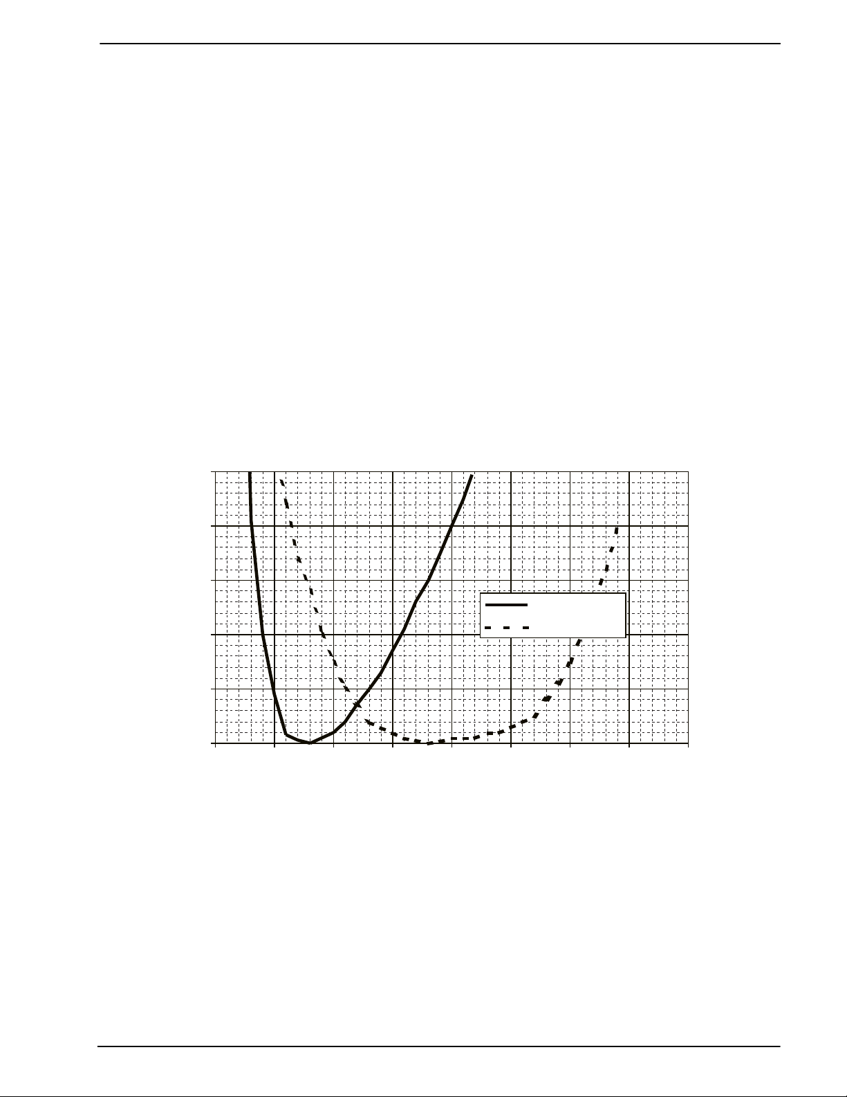
4.6 Equalizer
When receiving 1200bps FSK data an optional equalizer section can be enabled by setting Bit 6 of the FSK
MODE Register, compensates for one-half of the ETS Test Line 1 characteristics shown in Figure 6.
5
4
3
dB
ms
2
1
0
0 500 1000 1500 2000 2500 3000 3500 4000
Hz
Figure 6: ETS 300 114 Test Line 1 Characteristics (Normalized)
dB wrt 800Hz
ms wrt 1700Hz
1999 MX-COM, Inc. www.mxcom.com Tel: 800 638 5577 336 744 5050 Fax: 336 744 5054 Doc. # 20480180.108
4800 Bethania Station Road, Winston-Salem, NC 27105-1201 USA All trademarks and service marks are held by their respective companies.
Page 9

Bell 202 and V.23 Compatible Modem 9 CMX624 Preliminary Information
4.7 FSK Demodulator
The FSK Demodulator block is enabled when Bit 1 and Bit 5 of the FSK MODE Register are set to ‘1’. It
converts the 75bps, 150bps or 1200bps FSK input signal to a binary received data signal which is sent to the
Rx UART block.
Note: In the absence of a valid FSK signal, the demodulator may falsely interpret speech or other
extraneous signals as data.
FSK mode Register $E7 TX Tone Register $E1
Bit 5 Bit 4 Bit 0 RX MODE
1 1 0 RX FSK data at 1200 baud
1 0 0 Rx FSK data at 75/150 baud
0 X 0 RX Call progress Tones Detect
1 1 1 RX 2100Hz tone detect
Note: Other states are not defined and may result in unpredictable behavior
Table 4: Receive Mode
0
dB
-10
1200bps
-20
75/150 bps
Call Progress
-30
-40
100 1000 10000
Hz
Figure 7 Rx Frequency Responses with Line Interface
1999 MX-COM, Inc. www.mxcom.com Tel: 800 638 5577 336 744 5050 Fax: 336 744 5054 Doc. # 20480180.108
4800 Bethania Station Road, Winston-Salem, NC 27105-1201 USA All trademarks and service marks are held by their respective companies.
Page 10

Bell 202 and V.23 Compatible Modem 10 CMX624 Preliminary Information
4.8 Rx Energy and 2100Hz Detector
The Rx Energy and 2100Hz Detector functional blocks are controlled by Bit 4 and Bit 5 of the FSK MODE
Register and Bit 0 of the TX TONES Register.
This block will measure the frequency and amplitude of the incoming signal when Bit 0 of the TX TONES
Register and Bit 4 and Bit 5 of the FSK MODE Register are set to ‘1’. When a signal of 2100Hz is present
and of sufficient amplitude and time, Bit 4 of the FLAGS Register is set high. See Section 6.1 for amplitude,
time and frequency limits.
When Bit 0 of the TX TONES Register is set to ‘0’, this block compares the signal level at the output of the
Receive Filter against an internal threshold. This may be used as a FSK level detector or a simple Call
Progress Signal detector, according to the settings of Bit 4 and Bit 5 of the FSK MODE Register, which affect
the Receive Filter pass band as described in Section 4.5.
The required register settings are summarized in Table 5.
TX TONES Reg FSK MODE Reg
Bit 0 Bit 5 Bit 4 Detection Mode
0 0 0 Call Progress
0 1 0 75 / 150bps FSK
0 1 1 1200bps FSK
1 1 1 2100Hz
Table 5: Required Register Settings
Bit 4 of the FLAGS Register is set to ‘1’ by the output of this block when the received level has exceeded the
threshold for sufficient time. Amplitude and time hysteresis, are used to reduce chattering in marginal
conditions. See Section 6.1.
Received
Line Signal
B4 of FLAGS
Register
Te
FSK or Call Progress Signal
ON
Te
OFF
Figure 8: Rx Energy Detector Timing
4.9 FSK / DTMF Modulator
When Bit 7 of the TX TONES Register is set to ‘0’ then the FSK/DTMF Modulator generates FSK signals as
determined by Bit 0 and Bit 1 of the FSK MODE Register and the Tx data bits from the UART block as shown
in Table 6 and Table 7.
4.9.1 V.23 mode (Bit 7 of SETUP register = ‘0’):
FSK MODE
Reg
Bit 1 Bit 0 (Bit 7 of TX TONES = ‘0’) ‘0’ (Space) ‘1’ (Mark)
0 x Disabled (output held at VDD/2)
1 0 75bps FSK 450Hz 390Hz
1 1 1200bps FSK 2100Hz 1300Hz
FSK / DTMF Modulator block output FSK Signal Frequency
Table 6: V.23 mode (Bit 7 of SETUP register = ‘0’)
1999 MX-COM, Inc. www.mxcom.com Tel: 800 638 5577 336 744 5050 Fax: 336 744 5054 Doc. # 20480180.108
4800 Bethania Station Road, Winston-Salem, NC 27105-1201 USA All trademarks and service marks are held by their respective companies.
Page 11

Bell 202 and V.23 Compatible Modem 11 CMX624 Preliminary Information
4.9.2 Bell 202 mode (Bit 7 of SETUP register = ‘1’):
FSK MODE
FSK / DTMF Modulator block output FSK Signal Frequency
Reg
Bit 1 Bit 0 (Bit 7 of TX TONES = ‘0’) ‘0’ (Space) ‘1’ (Mark)
0 x Disabled (output held at VDD/2)
1 0 150bps FSK 487Hz 387Hz
1 1 1200bps FSK 2200Hz 1200Hz
Table 7: Bell 202 mode (Bit 7 of SETUP register = ‘1’)
When Bit 7 of the TX TONES Register is set to ‘1’, the block generates DTMF tone pairs or single tones from
the DTMF range as shown in Table 8. Bit 6 of the TX TONES Register is then used to enable or disable the
block’s output to the Tx filter.
TX DATA Register TX TONES Register
Bits 0 - 3
D3 D2 D1 D0 Lower
Frequency (Hz)
DTMF Tone Pairs
(Bit 4 = ‘0’)
Upper
Frequency (Hz)
Keypad
Legend
Single Tone
(Bit 4 = ‘1’)
Single Tone
Frequency (Hz)
0000 941 1633 D 1633
0001 697 1209 1 1209
0010 697 1336 2 1336
0011 697 1477 3 1477
0100 770 1209 4 1209
0101 770 1336 5 1336
0110 770 1477 6 1477
0111 852 1209 7 1209
1000 852 1336 8 852
1001 852 1477 9 852
1010 941 1336 0 941
1011 941 1209 * 941
1100 941 1477 # 941
1101 697 1633 A 697
1110 770 1633 B 770
1111 852 1633 C 852
Table 8: DTMF Transmitting settings
1999 MX-COM, Inc. www.mxcom.com Tel: 800 638 5577 336 744 5050 Fax: 336 744 5054 Doc. # 20480180.108
4800 Bethania Station Road, Winston-Salem, NC 27105-1201 USA All trademarks and service marks are held by their respective companies.
Page 12

Bell 202 and V.23 Compatible Modem 12 CMX624 Preliminary Information
4.10 Transmit Filter
This stage attenuates out of band signals present at the output of the FSK/DTMF modulator and also includes
a programmable 3dB level switch, selected by Bit 2 of the FSK MODE Register.
The nominal output levels at the TX pin when V
= 5.0V are as shown below.
DD
FSK MODE
Register Bit 2
FSK Signal DTMF Tone
(Low group)
DTMF Tone
(High group)
0 (low level) -6dB -5dB -3dB
1 (high level) -3dB -2dB 0dB
0dB = 775mV
RMS
Table 9: Transmit Filter
These levels are proportional to V
, and the actual transmit signal levels present on the 2- or 4-wire line will
DD
depend on the external circuitry as described in Section 5.1. Using the external components recommended in
Section 5.1 for a nominal FSK transmit level of -9dBm, DTMF tone levels of -8dBm and -6dBm, then the out
of band energy sent to the line will be within the limits shown in Figure 9 for both FSK and DTMF signals.
0
-10
-20
-30
dBm
-40
-50
Bell 202
V23
-60
-70
10 100 1000 10000 100000
Hz
Figure 9: Maximum Out of Band Tx Line Energy Limits
4.11 Transmit Output Buffer
This buffer amplifier, connected to the TXIN-, TX+ and TX- pins, is intended for use as a Tx line driver as
shown in
Section 5.1. Two symmetrical outputs are provided for use with a balanced load to give sufficient Tx line
signal levels even at low
. If this is not required the TX- output can be disabled.
V
DD
If the buffer is used as a balanced line driver, then Bit 6 of the SETUP Register should be set to ‘1’ (TXoutput enabled). Setting Bit 6 to ‘0’ disables the TX- output and the buffer draws less current from the supply.
When Bit 6 is set to '0' the TX- pin should be left open circuit. N.B. The TX+ output is unaffected by this Bit.
4.12 Ring Signal Detector
This block, which functions even in Zero Power mode, can be used to detect a telephone line Ring Signal or
Line Voltage Reversal and then generate a Interrupt Request signal to wake up the µC at the start of a call.
Suitable interface circuits are shown in Section 5.2.
The output of this block is the ‘Ring Detect’ line shown in Figure 1, which directly drives Bit 6 of the FLAGS
Register. Any ‘0’ to ‘1’ or ‘1’ to ‘0’ change on this line will also set the Ring Detect Change Bit (5) of the
FLAGS Register.
If this block is not used, then the RD and RT pins should be connected to V
Change Bit (5) of the IRQ MASK Register set to ‘0’.
and the Ring Detect
SS
1999 MX-COM, Inc. www.mxcom.com Tel: 800 638 5577 336 744 5050 Fax: 336 744 5054 Doc. # 20480180.108
4800 Bethania Station Road, Winston-Salem, NC 27105-1201 USA All trademarks and service marks are held by their respective companies.
Page 13

Bell 202 and V.23 Compatible Modem 13 CMX624 Preliminary Information
4.13 Tx/Rx UART
This block connects the µC, via the Serial Bus interface, to the received data from the FSK Demodulator and
to the transmit data input to the FSK Modulator.
As part of this function, the block can be programmed to convert data to be transmitted from 7 or 8-Bit bytes
to asynchronous data characters, adding Start and Stop bits and - optionally - a parity bit to the data before
passing it to the FSK Modulator. Similarly, in the receive direction it can extract data bits from asynchronous
characters coming from the FSK Demodulator, stripping off the Start and Stop bits and performing an optional
Parity check on the received data before passing the result over the Serial Bus to the µC. Bits 0-3 of the
SETUP Register control the number of Stop and Data bits and the Parity options for both receive and transmit
directions.
Data to be transmitted should be loaded by the µC into the TX DATA Register when the Tx Data Ready bit
(Bit 0) of the FLAGS Register goes high. It will then be treated by the Tx UART block in one of two ways,
depending on the setting of Bit 3 of the FSK MODE Register:
1. If the bit is ‘0’ (‘Tx Sync’ mode) then the 8 bits from the TX DATA Register will be transmitted sequentially
at 75bps, 150bps, or 1200bps, LSB (D0) first.
2. If Bit 3 of the FSK MODE Register is ‘1’ (‘Tx Async’) then bits will be transmitted as asynchronous data
characters at 75bps, 150bps, or 1200bps according to the following format:
A. One Start bit (Space).
B. 7 or 8 Data bits from the TX DATA Register (D0-D6 or D0-D7) as determined by Bit 0 of the
SETUP Register. LSB (D0) transmitted first.
C. Optional Parity bit (even or odd parity) as determined by Bits 1 and 2 of the SETUP Register.
D. One or Two Stop bits (Mark) as determined by Bit 3 of the SETUP Register.
In both cases data will only be transmitted if Bit 1 of the FSK MODE Register is set to ‘1’.
Failure to load the TX DATA Register with a new value when required will result in Bit 1 (Tx Data Underflow)
of the FLAGS Register being set to ‘1’ and if the ‘Tx Async’ mode of operation had been selected then a
continuous Mark (‘1’) signal will then be transmitted until a new value is loaded into TX DATA, whereas in ‘Tx
Sync’ mode the byte already in the TX DATA Register will be re-transmitted.
Tx FSK signal:
T
TBD
TX DAT A Register loaded:
Tx Data Ready flag bit:
Tx Data Underflow flag bit:
P'ty
T
Stop
TBD
D0 D0
Start Start
T
TBD
D1 D2
D3
D4
D5 D6
D7
Figure 10: Transmit UART Function (Async)
1999 MX-COM, Inc. www.mxcom.com Tel: 800 638 5577 336 744 5050 Fax: 336 744 5054 Doc. # 20480180.108
4800 Bethania Station Road, Winston-Salem, NC 27105-1201 USA All trademarks and service marks are held by their respective companies.
Page 14

Bell 202 and V.23 Compatible Modem 14 CMX624 Preliminary Information
Received data from the FSK Demodulator goes into the receive part of the UART block, where it is handled in
one of two ways depending on the setting of Bit 7 of the FSK MODE Register:
1. If the bit is ‘0’ (‘Rx Sync’ mode) then the receive part of the UART block will simply take 8 consecutive bits
from the Demodulator and transfer them to the RX DATA Register (the first bit going into the D0 position).
Note: This mode is intended for detection of simple data patterns such as ‘1010…’ or continuous Mark
or Space signals, the CMX624’s receive data clock extraction circuits are not adequate to support
a true synchronous receive data mode of operation.
2. If Bit 7 of the FSK MODE Register is ‘1’ (‘ Rx Async’) then the received data output of the FSK
Demodulator is treated as 75, 150 or 1200bps asynchronous characters each comprising:
A. A Start bit (Space).
B. 7 or 8 Data bits as determined by Bit 0 of the SETUP Register. These bits will be placed into the
RX DATA Register with the first bit received going into the D0 position.
C. An optional Parity bit as determined by Bits 1 and 2 of the SETUP Register. If Parity is enabled
(Bit 2 of the SETUP Register = ‘1’) then Bit 7 of the FLAGS Register will be set to ‘1’ if the
received parity is incorrect.
D. At least one Stop bit (Mark).
Bit 2 (Rx Data Ready) of the FLAGS Register will be set to ‘1’ every time a new received value is loaded into
the RX DATA Register. If the previous contents of the RX DATA Register had not been read out over the
Serial Bus before the new value is loaded from the UART then Bit 3 (Rx Data Overflow) of the FLAGS
Register will also be set to ‘1’.
Rx FSK signal:
RX DATA Register read
Rx Data Ready flag bit:
Rx Data Overflow flag bit:
P'ty
T
Stop
TBD
D0 D0
Start Start
D1 D2
D3
D4
D5 D6
D7
Figure 11: Receive UART Function (Async)
1999 MX-COM, Inc. www.mxcom.com Tel: 800 638 5577 336 744 5050 Fax: 336 744 5054 Doc. # 20480180.108
4800 Bethania Station Road, Winston-Salem, NC 27105-1201 USA All trademarks and service marks are held by their respective companies.
Page 15

Bell 202 and V.23 Compatible Modem 15 CMX624 Preliminary Information
5 Application Notes
5.1 Line Interface
A line interface circuit is needed to provide DC isolation between the modem and the line, to perform line
impedance termination, and to set the correct transmit and receive signal levels.
5.1.1 4-Wire Line Interface
Figure 12 shows an interface circuit for use with a 600Ω 4-wire line. The line terminations are provided by
R10 and R15, while R11 and R13 should be selected to give the desired transmit and receive levels.
5.1.1.1 Receive Gain
The gain of the receive input amplifier (R12 / R11) should be set to compensate for the loss of the input
transformer and the supply voltage.
Assuming a transformer loss of about 1dB, R11 should be 91kΩ at V
RXAMPOUT
= 5.0V, or 130kΩ at 3.3V.
DD
4-Wire
Line
Rx
Tx
1:1
1:1
A
C10
R10
R12
R11
V
R13
R14
R15
BIAS
C13
C11
RX-
RX+
TX
TXIN-
C12
TX+
TX-
-
+
CMX624
-
+
V
BIAS
-
+
V
BIAS
Figure 12: 4-Wire Line Interface Circuit
R10
Ω±
600
R11 See text
R12
100k
Ω±
R13 See text
R14
100k
Ω±
±
±
1%
1%
1%
1%
1%
R15
Ω±
600
C10 100nF
C11 220pF
C12 330pF
C13 100nF
±
20%
±
20%
±
20%
±
20%
1%
Tolerances for Resistors and Capacitors are as indicated unless otherwise stated.
Table 10: 4-Wire Line Interface Circuit components
Note: The relay circuit, AC and DC loads and line protection are not shown for clarity.
1999 MX-COM, Inc. www.mxcom.com Tel: 800 638 5577 336 744 5050 Fax: 336 744 5054 Doc. # 20480180.108
4800 Bethania Station Road, Winston-Salem, NC 27105-1201 USA All trademarks and service marks are held by their respective companies.
Page 16

Bell 202 and V.23 Compatible Modem 16 CMX624 Preliminary Information
g
g
5.1.1.2 Transmit Gain
In the transmit direction, the level on the 4-wire line is determined by the level at the TX pin, the gain of the
Output Buffer Amplifier, a loss of nominally 6dB due to the line termination resistor R15, and the loss in the
transformer.
The TX pin signal level is proportional to V
and is also affected by the setting of the Tx output level control
DD
Bit (Bit 2) of the FSK Mode Register.
Assuming that the Tx output level control bit is set to ‘1’ (giving a FSK signal level of -3dB with respect to
775mV
at the TX pin when VDD = 5.0V) and that there is 1dB loss in the transformer, then:
RMS
14R2
()
20163 level line rewi fourFSK Tx
lo
×+−−−=
×
13R
20
lo
×+
1010
V
DD
dBm
0.5
For example, to generate a nominal Tx FSK line level of -9dBm, R13 should be 180kΩ when V
= 5.0V,
DD
falling to 120kΩ at 3.3V.
5.1.2 2-Wire Line Interface
Figure 13 shows an interface circuit suitable for connection to a 600Ω 2-wire line. The circuit also shows how
a relay may be driven from the RLYDRV pin.
Note: When the CMX624 is powered from less than 5.0V, buffer circuitry may be required to drive a 5V
relay.
RXAMPOUT
C11
RXRX+
RLYDRV
C14
TX
R13
TXIN-
C12
TX+
TX-
-
+
CMX624
-
+
V
BIAS
-
+
V
BIAS
2-Wire
Line
To Ring
Detect
Circuit
See 5.2
+ve
1:1
R16
R15
R12
R11
R17
C13
R14
Figure 13: 2-Wire Line Interface Circuit
R11 See text
R12
Ω±
100k
R13 See text
R14
R15
R16
Ω±
100k
Ω±
600
Ω±
120k
±
±
1%
1%
1%
1%
1%
1%
R17
100k
C11 220pF
C12 330pF
C13 10nF
C14 100nF
Ω±
±
20%
±
20%
±
20%
±
20%
1%
Tolerances for Resistors and Capacitors are as indicated unless otherwise stated.
Table 11: 2-Wire Line Interface Circuit components
Note: The relay circuit, AC and DC loads and line protection are not shown for clarity.
This circuit includes a 2-wire to 4-wire hybrid circuit, formed by R11, R15, R16, R17, C13 and the impedance
of the line itself, which ensures that the modem receive input and transmit output paths are both coupled
efficiently to the line, while minimizing coupling from the modem’s transmit signal into the receive input.
The values of R11 and R13 should be calculated in the same way as for the 4-wire interface circuit of
Figure 12.
1999 MX-COM, Inc. www.mxcom.com Tel: 800 638 5577 336 744 5050 Fax: 336 744 5054 Doc. # 20480180.108
4800 Bethania Station Road, Winston-Salem, NC 27105-1201 USA All trademarks and service marks are held by their respective companies.
Page 17

Bell 202 and V.23 Compatible Modem 17 CMX624 Preliminary Information
5.2 Ring Detector Interface
Figure 14 shows how the CMX624 may be used to detect large amplitude Ringing signals received at the
start of an incoming telephone call.
The ring signal is applied at the subscriber's exchange as an AC voltage inserted in series with one of the
telephone wires and will pass through either C20 and R20 or C21 and R21 to appear at the top end of R22 in
a rectified and attenuated form. See point X in Figure 14.
The signal at point X is further attenuated by the R22 and R23 divider before being applied to the RD input. If
the amplitude of the signal appearing at RD is greater than the input threshold (Vt
the transistor (Q1) connected to RT will be turned on, pulling the voltage at RT to V
external capacitor C22. The output of the Schmitt trigger 'B' will then go high, setting bit 6 (Ring Detect) of the
FLAGS register.
The minimum amplitude ringing signal that is certain to be detected is found by the following calculation:
) of Schmitt trigger 'A' then
HI
by discharging the
SS
where Vt
[]
HI
+
7.0
is the high-going threshold voltage of the Schmitt trigger A. See Figure 15 and Section 6.1.3.
HI
++×
23R22R20RVt
23R
=×
VSignal Ring .MinV707.0
RMSRMS
With R20-22 at 470kΩ as shown Figure 14, then setting R23 to 68kΩ will guarantee detection of ringing
signals of 40V
2-Wire
Telephone
and above for VDD over the range 3.0 to 5.5V.
RMS
C20
R20
X
R22
D1 - 4
RD
CMX624
A
Q1
B
To FLAGS
register
Line
R23
R21
C22
RT
R24C21
V
DD
Ring signal
Bridge rectifier output (X)
RT
Vt
HI
V
SS
Vt
HI
V
SS
FLAGS register bit 6
(RING DETECT)
FLAGS register bit 5
(RING DETECT Change)
Figure 14: Ring Signal Detector Interface Circuit
R20,21,22
R23 See text
R24 Note 1
Ω±
470k
Ω±
470k
±
1%
1%
1%
Tolerances for Resistors and Capacitors are as indicated unless otherwise stated.
Table 12: Ring Signal Detector Interface Circuit components
1999 MX-COM, Inc. www.mxcom.com Tel: 800 638 5577 336 744 5050 Fax: 336 744 5054 Doc. # 20480180.108
4800 Bethania Station Road, Winston-Salem, NC 27105-1201 USA All trademarks and service marks are held by their respective companies.
C20,21
C22 Note 1
0.1µF
0.33µF
D1-4 1N4004
±
20%
±
20%
±
20%
Page 18

Bell 202 and V.23 Compatible Modem 18 CMX624 Preliminary Information
Note:
1. If the time constant of R24 and C22 is large enough then the voltage on RT will remain below the
threshold of the 'B' Schmitt trigger for the duration of a ring cycle.
The time for the voltage on RT to charge from V
=
towards VDD can be derived from the formula:
SS
t
−
DDRT
22xC24R
e-1VV
As the Schmitt trigger high-going input threshold voltage (VtHI) has a minimum value of 0.56 x VDD, then
the Schmitt trigger B output will remain high for a time of at least 0.821 x R24 x C22 following a pulse at
RD.
The values of R24 and C22 given in Figure 14 (470kΩ and 0.33µF) give a minimum RT charge time of
100ms, which is adequate for ring frequencies of 10Hz or above.
Note: The circuit will also respond to a telephone line voltage reversal. If necessary the µC can distinguish
between a Ring signal and a line voltage reversal by measuring the time that bit 6 of the FLAGS
register (Ring Detect) is high.
1999 MX-COM, Inc. www.mxcom.com Tel: 800 638 5577 336 744 5050 Fax: 336 744 5054 Doc. # 20480180.108
4800 Bethania Station Road, Winston-Salem, NC 27105-1201 USA All trademarks and service marks are held by their respective companies.
Page 19

Bell 202 and V.23 Compatible Modem 19 CMX624 Preliminary Information
6 Performance Specification
6.1 Electrical Performance
6.1.1 Absolute Maximum Ratings
Exceeding these maximum ratings can result in damage to the device.
Min. Max. Unit
Supply (VDD - VSS) -0.3 7.0 V
Voltage on any pin to V
SS
Current
V
DD
V
SS
Any other pin -20 20 mA
RLYDRV pin 50 mA
D2 / P4 Package Min. Max. Unit
Total Allowable Power Dissipation at T
= 25°C 800 mW
AMB
Derating above 25°C 13 mW/°C above 25°C
Storage Temperature -55 125 °C
Operating Temperature -40 85 °C
D5 Package Min. Max. Unit
Total Allowable Power Dissipation at T
= 25°C 550 mW
AMB
Derating above 25°C 9 mW/°C above 25°C
Storage Temperature -55 125 °C
Operating Temperature -40 85 °C
-0.3 V
+ 0.3 V
DD
-50 50 mA
-50 50 mA
6.1.2 Operating Limits
Correct operation of the device outside these limits is not implied.
Notes Min. Max. Unit
Supply (VDD - VSS)2.75.5V
Operating Temperature -40 85 °C
Xtal Frequency 1 3.575965 3.583125 MHz
Notes: A Xtal frequency of 3.579545MHz ±0.1% is required for correct operation.
1999 MX-COM, Inc. www.mxcom.com Tel: 800 638 5577 336 744 5050 Fax: 336 744 5054 Doc. # 20480180.108
4800 Bethania Station Road, Winston-Salem, NC 27105-1201 USA All trademarks and service marks are held by their respective companies.
Page 20

Bell 202 and V.23 Compatible Modem 20 CMX624 Preliminary Information
6.1.3 Operating Characteristics
For the following conditions unless otherwise specified:
V
= 2.7V at T
DD
Xtal Frequency = 3.579545MHz ± 0.1%, 0dBm corresponds to 775mV
= 25°C and V
AMB
= 3.0V to 5.5V at T
DD
= -40 to 85°C,
AMB
RMS
.
Notes Min. Typ. Max. Unit
DC Parameters
IDD (Zero Power mode) 1, 2 1.0
µ
A
(Running, TX- output Off, VDD= 5.0V) 1 3.4 6.0 mA
(Running, TX- output Off, VDD= 3.3V) 1 1.8 3.2 mA
(Running, TX- output On, VDD= 5.0V) 1 3.5 6.2 mA
(Running, TX- output On, VDD= 3.3V) 1 1.9 3.4 mA
Logic '1' Input Level 3 70% V
Logic '0' Input Level 3 30% V
Logic Input Leakage Current
(Vin = 0 to V
), (excluding
DD
-1.0 1.0
DD
DD
µ
A
XTAL/CLOCK input)
V
Output Logic '1' Level (lOH = 360µA)
Output Logic '0' Level (l
IRQ
OUTPUT 'Off' State Current
(V
= VDD)
OUT
= 360µA)
OL
Schmitt trigger input high-going
threshold (Vt
) (see Figure 15)
HI
Schmitt trigger input low-going
threshold (Vt
) (see Figure 15)
LO
RLYDRV ‘ON’ resistance
to V
(VDD= 5.0V)
SS
(0.44)V
-0.4 V
DD
0.4 V
1.0
(0.56)V
DD
DD
- 0.6V (0.44)V
(0.56)V
+ 0.6V V
DD
DD
38.0 TBD
µ
A
V
Ω
FSK Modulator and Tx UART
Level at TX pin. 4 -4.0 -3.0 -2.0 dBm
Twist (Mark level WRT Space level) -2.0 0 2.0 dB
Tx 1200bps (V.23 mode)
Baud Rate (set by UART and Xtal
1194 1200 1206 Baud
frequency)
Mark (Logical 1) Frequency 1297 1300 1303 Hz
Space (Logical 0) Frequency 2097 2100 2103 Hz
Tx 75bps (V.23 mode)
Baud Rate (set by UART and Xtal
74 75 76 Baud
frequency)
Mark (Logical 1) Frequency 388 390 392 Hz
Space (Logical 0) Frequency 448 450 452 Hz
Tx 1200bps (Bell 202 mode)
Baud Rate (set by UART and Xtal
1194 1200 1206 Baud
frequency)
Mark (Logical 1) Frequency 1197 1200 1203 Hz
Space (Logical 0) Frequency 2197 2200 2203 Hz
1999 MX-COM, Inc. www.mxcom.com Tel: 800 638 5577 336 744 5050 Fax: 336 744 5054 Doc. # 20480180.108
4800 Bethania Station Road, Winston-Salem, NC 27105-1201 USA All trademarks and service marks are held by their respective companies.
Page 21

Bell 202 and V.23 Compatible Modem 21 CMX624 Preliminary Information
Notes Min. Typ. Max. Unit
Tx 150bps (Bell 202 mode)
Baud Rate (set by UART and Xtal
149 150 151 Baud
frequency)
Mark (Logical 1) Frequency 385 387 389 Hz
Space (Logical 0) Frequency 485 487 489 Hz
DTMF Transmitter
Level at TX pin; tones in High Group 4 -1.0 0.0 1.0 dBm
Twist (level of High Group tones with
2.0 dB
respect to level of Low Group tones)
Tone frequency accuracy (worst case) -0.5 0.5 %
Tx Filter and Output Buffer
Change in level at TX pin caused by
2.5 3.0 3.5 dB
changing Bit 2 of FSK MODE Register
Buffer output signal swing;
5 2.2 V
P-P
Load ≥ 500Ω.
FSK Demodulator and Rx UART
Valid Input Level Range 6 -43.0 -9.0 dBm
Acceptable Twist
-7.0 7.0 dB
(Mark level with respect to Space level)
Acceptable Signal to Noise Ratio 7 20.0 - dB
Rx 1200bps (V.23 mode)
Acceptable Rx Data Rate 8 1188 1200 1212 Baud
Mark (Logical 1) Frequency 1280 1300 1320 Hz
Space (Logical 0) Frequency 2068 2100 2132 Hz
Rx 75bps (V.23 mode)
Acceptable Rx Data Rate 8 TBD 75 TBD Baud
Mark (Logical 1) Frequency TBD 390 TBD Hz
Space (Logical 0) Frequency TBD 450 TBD Hz
Rx 1200bps (Bell 202 mode)
Acceptable Rx Data Rate 8 1188 1200 1212 Baud
Mark (Logical 1) Frequency 1180 1200 1220 Hz
Space (Logical 0) Frequency 2168 2200 2232 Hz
Rx 150bps (Bell 202 mode)
Acceptable Rx Data Rate 8 TBD 150 TBD Baud
Mark (Logical 1) Frequency TBD 387 TBD Hz
Space (Logical 0) Frequency TBD 487 TBD Hz
2100Hz Detector
‘Will Decode’ Frequency Range 2040 2235 Hz
‘Will Not Decode’ Frequency Range <2010 >2265 Hz
‘Off’ to ‘On’ time 9 25 ms
‘On’ to ‘Off’ time 9 4.0 ms
1999 MX-COM, Inc. www.mxcom.com Tel: 800 638 5577 336 744 5050 Fax: 336 744 5054 Doc. # 20480180.108
4800 Bethania Station Road, Winston-Salem, NC 27105-1201 USA All trademarks and service marks are held by their respective companies.
Page 22

Bell 202 and V.23 Compatible Modem 22 CMX624 Preliminary Information
Notes Min. Typ. Max. Unit
Rx Energy Detector
‘Off’ to 'On' Threshold Level 6, 10 -48.0 -43.0 dBm
Hysteresis (measured at VDD = 3.0V
and V
= 5.0V)
DD
6, 10 2.0 dB
'Off' to 'On' Time (Figure 8 TeON): 6, 10
1200bps Rx mode 25 ms
75/150bps Rx mode 48 ms
Call Progress Detect mode 48 ms
'On' to 'Off' Time (Figure 8 Te
): 6, 10
OFF
1200bps Rx mode 8.0 ms
75/150bps Rx mode 20 ms
Call Progress Detect mode 20 ms
XTAL/CLOCK Input
'High' Pulse Width 11 100 ns
'Low' Pulse Width 11 100 ns
Notes:
1. At 25°C, not including any current drawn from the CMX624 pins by external circuitry other than X1, C1,
and C2.
2. All logic inputs at V
except for RT and CS inputs, which are at VDD.
SS
3. Excluding RD, RT and XTAL/CLOCK pins.
4. At V
5. For each of the TX- (if enabled) and TX+ pins, load between pin and V
6. Measured at the Rx Input Amplifier output (pin RXAMPOUT) for V
= 5.0V, Tx output level control bit set to ‘1’; load resistance greater than 40kΩ.
DD
/2.
DD
= 5.0V.
DD
The internal threshold levels are proportional to VDD. To cater for other supply voltages or different signal
level ranges the voltage gain of the Rx Input Amplifier should be adjusted by selecting the appropriate
external components as described in Section 5.1.
7. Flat noise in 300-3400 Hz band for V.23, 200-3400 Hz for Bell 202.
8. Set by Rx UART and Xtal frequency.
9. 2100Hz detection requires a signal within the amplitude range given in Section 4.5.
10. Measured with 1300Hz signal in 1200bps mode, 390Hz for 75bps or 150bps and Call Progress mode,
signal level -33dBm for time delay measurements.
11. Timing for an external input to the XTAL/CLOCK pin.
1999 MX-COM, Inc. www.mxcom.com Tel: 800 638 5577 336 744 5050 Fax: 336 744 5054 Doc. # 20480180.108
4800 Bethania Station Road, Winston-Salem, NC 27105-1201 USA All trademarks and service marks are held by their respective companies.
Page 23

Bell 202 and V.23 Compatible Modem 23 CMX624 Preliminary Information
3.5
3
2.5
2
Vin
1.5
1
0.5
Vthi
Vtlo
0
2.5 3 3.5 4 4.5 5 5.5
Vdd
Figure 15: Typical Schmitt Trigger Input Voltage Thresholds vs. V
DD
1999 MX-COM, Inc. www.mxcom.com Tel: 800 638 5577 336 744 5050 Fax: 336 744 5054 Doc. # 20480180.108
4800 Bethania Station Road, Winston-Salem, NC 27105-1201 USA All trademarks and service marks are held by their respective companies.
Page 24

Bell 202 and V.23 Compatible Modem 24 CMX624 Preliminary Information
6.1.4 Timing
Serial Bus Timings Description Notes Min. Typ. Max. Unit
t
CSE
t
CSH
t
LOZ
t
HIZ
t
CSOFF
t
NXT
t
CK
t
CH
t
CL
t
CDS
t
CDH
t
RDS
t
RDH
-Enable to Clock-High time
CS
Last Clock-High to CS-High time
Clock-Low to Reply Output enable time 0.0 ns
-High to Reply Output 3-state time
CS
-High Time between transactions
CS
Inter-Byte Time 200 ns
Clock-Cycle time 200 ns
Serial Clock-High time 100 ns
Serial Clock-Low time 100 ns
Command Data Set-Up time 75 ns
Command Data Hold time 25 ns
Reply Data Set-Up time 75 ns
Reply Data Hold time 0 ns
100 ns
100 ns
1.0 µs
1.0 µs
Note: These timings are for the latest version of the Serial Bus as embodied in the CMX624, and allow
faster transfers than the original Serial Bus.
CS
SERIAL CLOCK
COMMAND DATA
REPLY DA TA
70%V
DD
30%V
DD
COMMAND
DATA
t
CSE
76543
HI-Z
t
CL
t
CDS
t
CK
= Level not important or undefined
t
CH
t
CDH
t
NXT
21
t
LOZ
SERIAL
CLOCK
0 76543
Figure 16: Serial Bus Timing
76543
t
CK
t
RDS
REPLY
DATA
t
CSH
21
21
t
RDH
t
CSOFF
0
t
HIZ
0
1999 MX-COM, Inc. www.mxcom.com Tel: 800 638 5577 336 744 5050 Fax: 336 744 5054 Doc. # 20480180.108
4800 Bethania Station Road, Winston-Salem, NC 27105-1201 USA All trademarks and service marks are held by their respective companies.
Page 25

Bell 202 and V.23 Compatible Modem 25 CMX624 Preliminary Information
6.2 Packaging
PackageTolerances
Alternative Pin
Location
Marking
Figure 17: 24-pin SOIC (D2) Mechanical Outline:
PIN 1
H
PIN 1
Y
H
Y
A
B
E
W
X
K
C
P
J
Z
A
0.597 (15.16)
B
0.286 (7.26)
0.093 (2.36)
C
0.390 (9.90)
E
H
0.013 (0.33)
L
T
J
0.036 (0.91)
K
0.016 (0.41)
L
P
0.009 (0.23)
T
W
X
Y
Z
NOTE: All dimensions in inches (mm.)
Angles are in degrees
0°
5°
TYP. MAX.MIN.DIM.
0.050 (1.27)
45°
5°
0.613 (15.57)
0.299 (7.59)
0.105 (2.67)
0.419 (10.64)
0.020 (0.51)0.003 (0.08)
0.020 (0.51)
0.046 (1.17)
0.050 (1.27)
0.0125 (0.32)
10°
7°
Order as part no. CMX624D2
A
B
Z
E
L
T
X
C
P
J
PackageTolerances
DIM.
A
0.318 (8.07)
B
0.205 (5.20)
C
E
0.301 (7.65)
H
J
0.010 (0.25) 0.015 (0.38)
L
0.022 (0.55)
P
T
0.005 (0.13) 0.009 (0.22)
X
Y
Z
NOTE: All dimensions in inches (mm.)
Angles are in degrees
TYP.
0.328 (8.33)
0.213 (5.39)
0.079 (2.00)0.066 (1.67)
0.312 (7.90)
0.008 (0.21)0.002 (0.05)
0.037 (0.95)
0.026 (0.65)
0°
7°
4°
MAX.MIN.
8°
9°
10°
Figure 18: 24-pin SSOP (D5) Mechanical Outline:
AA
BB
E1E1
Y
PIN1PIN1
K
H
CC
L
PP
JJ
J1J1
Figure 19: 24-pin PDIP (P4) Mechanical Outline:
TT
Order as part no. CMX624D5
PackageTolerances
A
EE
1.200 (30.48)
B
0.500 (12.70)
0.151 (3.84)
C
0.600 (15.24)
E
0.590 (14.99) 0.625 (15.88)
E1
0.015 (0.38) 0.045 (1.14)
H
0.015 (0.38) 0.023 (0.58)
J
0.040 (1.02) 0.065 (1.65)
J1
0.066 (1.67) 0.074 (1.88)
K
0.121 (3.07)
L
P
0.008 (0.20) 0.015 (0.38)
T
Y
NOTE: All dimensions in inches (mm.)
Angles are in degrees
Order as part no. CMX624P4
TYP. MAX.MIN.DIM.
1.270 (32.26)
0.555 (14.04)
0.220 (5.59)
0.670 (17.02)
0.160 (4.05)
0.100 (2.54)
7°
1999 MX-COM, Inc. www.mxcom.com Tel: 800 638 5577 336 744 5050 Fax: 336 744 5054 Doc. # 20480180.108
4800 Bethania Station Road, Winston-Salem, NC 27105-1201 USA All trademarks and service marks are held by their respective companies.
 Loading...