

Page 1
CMX469A
1200/2400/4800 Baud
FFSK/MSK Modem
2001 Consumer Microcircuits Limited
D/469A/2 May 2001 Provisional Issue
Features Applications
•• Full-Duplex FFSK/MSK Modem with
Separate Rx and Tx Enable Functions
•• Data-Over Radio
•• Personal/Cordless Telephone
•• Pin Selectable Data Rates:
1200, 2400 or 4800 Baud
•• Radio and General Applications
•• Narrowband Coax Data Channels
•• Pin Selectable Xtal/Clock Inputs:
1.008MHz or 4.032MHz
•• Two Way Radio (MPT1327) Signalling
•• Portable Data Terminals
•• Clock Recovery Facility
•• Carrier Detect Facility
•• Low Power Operation (2.0mA typ. at 3.0V)
1.1 Brief Description
The CMX469A is a single-chip CMOS LSI circuit which operates as a full-duplex 1200, 2400 or
4800 baud FFSK/MSK modem. The mark and space frequencies are 1200/1800, 1200/2400 and
2400/4800 Hz respectively. Tone frequencies are phase continuous; transitions occur at the zero
crossing point. A common Xtal oscillator with a choice of two clock frequencies (1.008MHz or
4.032MHz) provides baud-rate, transmit frequencies, and Rx and Tx synchronization.
The transmitter and receiver operate entirely independently, including the individual section
powersave functions. The CMX469A includes on-chip circuitry for Carrier Detect and Rx Clock
recovery, both of which are made available as output pins. Rx, Tx and Carrier Detect paths
contain bandpass filters to optimise signal conditions in each section of the modem. The
CMX469A demonstrates good sensitivity and bit-error-rate under adverse signal conditions. The
Carrier Detect time constant is set by an external capacitor, so that the product's performance
can be optimised in high noise environments. This low-power device operates from a single
supply between 2.7V and 5.5V, requires few external components and is available in a wide
variety of plastic packages.
Page 2

1200/2400/4800 Baud FFSK/MSK Modem CMX469A
2001 Consumer Microcircuits Limited 3 D/469A/2
CONTENTS
Section
Page
1.0 Features and Applications.......................................................................2
1.1 Brief Description .......................................................................................2
1.2 Block Diagram ...........................................................................................4
1.3 Signal List...................................................................................................5
1.4 External Components...............................................................................7
1.5 General Description..................................................................................8
1.6 Application Notes......................................................................................9
1.7 Performance Specification.....................................................................10
1.7.1 Electrical Performance..............................................................10
1.7.2 Packaging....................................................................................16
Page 3
1200/2400/4800 Baud FFSK/MSK Modem CMX469A
2001 Consumer Microcircuits Limited 4 D/469A/2
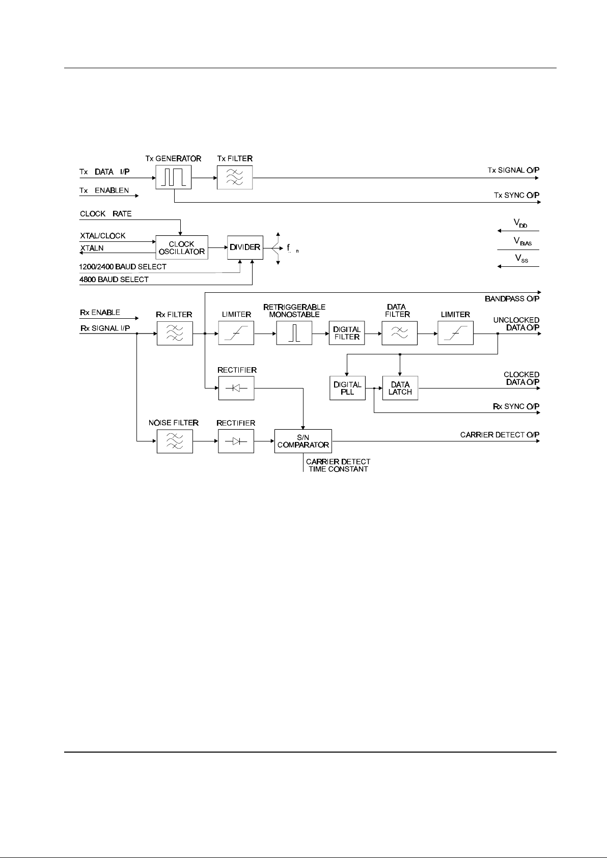
1.2 Block Diagram
Figure 1 Block Diagram
Page 4

1200/2400/4800 Baud FFSK/MSK Modem CMX469A
2001 Consumer Microcircuits Limited 5 D/469A/2
1.3 Signal List
CMX469A
D3 E2 P6 Signal Description
Pin
No.
Pin
No.
Pin
No.
Name Type
1 1 1 CLOCK/XTAL I/P The input to the on-chip inverter, for use with
either a 1.008MHz or a 4.032MHz Xtal or an
external clock. Clock frequency selection is by
means of the CLOCK RATE pin. This affects the
operational data rate of the device. Operation of
any CML microcircuit without a Xtal or clock
input may cause device damage.
2 2 2 XTALN O/P The output of the on-chip inverter.
3 3 3 Tx SYNC O/P O/P A squarewave, produced on-chip, to
synchronize the input of logic data and
transmission of the FFSK/MSK signal.
4 5 5 Tx SIGNAL
O/P
O/P When the transmitter is enabled, this pin outputs
the FFSK/MSK signal. With the transmitter
disabled, this pin is set to a high-impedance
state.
5 7 6 Tx DATA I/P I/P The serial logic data to be transmitted is input to
this pin.
6 8 7 Tx ENABLEN I/P A logic ‘0’ will enable the transmitter. A logic ‘1’ at
this input will put the transmitter into powersave
whilst forcing Tx SYNC OUTPUT to a logic ‘1’
and Tx SIGNAL OUTPUT to a high-impedance
state. This pin is internally pulled to V
DD
.
7 9 8 BANDPASS
O/P
O/P The output of the Rx Bandpass Filter. This output
impedance is typically 10k
Ω and may require
buffering prior to use.
8 10 9 Rx ENABLE I/P The control of the Rx function
9 11 10 V
BIAS
BI The output of the on-chip analogue bias circuitry.
Held internally at V
DD
/2, this pin should be
decoupled to V
SS
by a capacitor (C2). This bias
voltage is maintained under all powersave
conditions.
10 12 11 V
SS
PWR Negative supply rail (GND).
11 13 12 UNCLOCKED
DATA O/P
O/P The recovered asynchronous serial data output
from the receiver.
12 14 13 CLOCKED
DATA O/P
O/P The recovered synchronous serial data output
from the receiver. Data is latched out by the
recovered clock, available at the Rx SYNC O/P.
Page 5

1200/2400/4800 Baud FFSK/MSK Modem CMX469A
2001 Consumer Microcircuits Limited 6 D/469A/2
CMX469A
D3 E2 P6 Signal Description
Pin
No.
Pin
No.
Pin
No.
Name Type
13 15 14 CARRIER
DETECT O/P
O/P When an FFSK/MSK signal is being received
this output is a logic ‘1’.
14 16 15 Rx SIGNAL I/P I/P The FFSK/MSK signal input for the receiver. This
input should be coupled via a capacitor, C3.
15 18 17 Rx SYNC O/P O/P A flywheel squarewave output. This clock will
synchronize to incoming Rx FFSK/MSK data.
16 19 16 1200/2400
BAUD
SELECT
I/P A logic ‘1’ on this pin selects the 1200 baud
option. Tone frequencies are: one cycle of
1200Hz represents a logic ‘1,’ one-and-a-half
cycles of 1800Hz represents a logic ‘0.’
A logic ‘0’ on this pin selects the 2400 baud
option. Tone frequencies are: one-half cycle of
1200Hz represents a logic ‘1,’ one cycle of
2400Hz represents a logic ‘0.’ This function is
also used, in part, to select the 4800 baud
option. This pin has an internal 1M
Ω pullup
resistor.
17 20 18 4800 BAUD
SELECT
I/P A logic ‘1’ on this pin combined with a logic ‘0’ on
the 1200/2400 BAUD SELECT pin will select the
4800 baud option (1M
Ω pulldown resistor).
Tone frequencies are: one-half cycle of 2400Hz
represents a logic ‘1,’ one cycle of 4800Hz
represents a logic ‘0.’ Operation at 4800 baud is
only achieved by using a 4.032MHz Xtal or
clock.
18 21 19 CLOCK RATE I/P A logic input to select and allow the use of either
a 1.008MHz or 4.032MHz Xtal/clock. Logic ‘1’ =
4.032MHz, logic ‘0’ = 1.008MHz. This input has
an internal pulldown resistor (1.008MHz).
19 22 20 CARRIER
DETECT TIME
CONSTANT
BI Part of the carrier detect integration function. The
value of C4 connected to this pin will affect the
carrier detect response time and hence noise
performance.
20 24 22
V
DD
PWR Positive supply rail. A single 2.7 to 5.0 volt
supply is required. This pin should be decoupled
to V
SS
by a capacitor (C5).
4, 6,
17, 23
4, 21
No internal connection, do not use.
Notes: I/P = Input O/P = Output BI = Bidirectional PWR = Power
Page 6

1200/2400/4800 Baud FFSK/MSK Modem CMX469A
2001 Consumer Microcircuits Limited 7 D/469A/2
1.4 External Components
Component Value
R1
1.0MΩ
C1 33.0pF
C2 1.0µF
C3 0.1µF
C4 0.1µF
C5 1.0µF
C6 1.0µF
C7 33.0pF
X1 1.008MHz
or
4.032MHz
Notes:
1. V
BIAS
may be decoupled to VSS and VDD using C2 and C6 when input signals are referenced to the V
BIAS
pin. For input signals referenced to V
SS
, decouple V
BIAS
to VSS using C2 only.
2. The performance of the Carrier Detect function will be affected by the nature of the noise spectrum in the
received channel. The value of C4 determines the Carrier Detect Time Constant. A long time constant
results in improved noise immunity but increased response time. C4 may be varied to trade-off response
time for noise immunity.
3. A 4.032MHz Xtal/clock is required for 4800 Baud operation.
Figure 2 Recommended External Components
Page 7

1200/2400/4800 Baud FFSK/MSK Modem CMX469A
2001 Consumer Microcircuits Limited 8 D/469A/2
1.5 General Description
The CMX469A has two sections, apart from the Xtal oscillator circuit and clock dividers. These
sections may be independently powersaved.
Transmitter
The transmitter is enabled by taking Tx EnableN low. Serial data applied to Tx Data Input is sampled
internally and an FFSK/MSK sequence is generated. After filtering, this is output at
Tx Signal O/P and the transmit clock derived from this signal is output at Tx Sync O/P.
Receiver
The receiver is enabled by taking Rx Enable high. The signal applied to Rx Signal I/P is filtered and
recovered as serial data from the Unclocked Data O/P. A flywheel synchroniser is used to extract a
clock from the recovered serial data stream. The clock is available at Rx Sync O/P and the retimed
serial data is available at Clocked Data O/P.
The integrated peak values of the Rx amplitude are compared with out-of-band noise levels and used
to make a signal-to-noise assessment, which is available at Carrier Detect O/P.
A Bandpass O/P is also available from the output of the first Rx filter stage, but will require buffering
before use.
Page 8

1200/2400/4800 Baud FFSK/MSK Modem CMX469A
2001 Consumer Microcircuits Limited 9 D/469A/2
1.6 Application Notes
Rx Enable
The control of the relevant outputs with reference to the Rx Enable input is described below:
Rx Enable
Rx Function Clock Data O/P Carrier Detect O/P Rx Sync Out
‘1’ Enabled Enabled Enabled Enabled
‘0’ Powersave ‘0’ ‘1’ or ‘0’ ‘1’ or ‘0’
After enabling the Receiver, a time of at least 8 bit periods plus 2ms should be allowed for the Carrier Detect
circuit to stabilise and give a valid output.
Operational Data Rate Configurations
Operational Data Rate Configurations are as described below:
Xtal/Clock
Frequency
1.008MHz 4.032MHz
Clock Rate ‘0’
‘0’ ‘1’ ‘1’ ‘1’
1200/2400
Select
‘1’
‘0’ ‘1’ ‘0’ ‘0’
4800 Select ‘0’
‘0’ ‘0’ ‘0’ ‘1’
Baud Rate 1200
2400 1200 2400 4800
Test Set Up
Figure 3 Suggested CMX469A Test Set-Up
Page 9

1200/2400/4800 Baud FFSK/MSK Modem CMX469A
2001 Consumer Microcircuits Limited 10 D/469A/2
1.7 Performance Specification
1.7.1 Electrical Performance
Absolute Maximum Ratings
Exceeding these maximum ratings can result in damage to the device.
Min. Max. Units
Supply (VDD - VSS) -0.3 7.0 V
Voltage on any pin to V
SS
-0.3 V
DD
+ 0.3 V
Current into or out of VDD and V
SS
pins -30 +30 mA
Current into or out of any other pin -20 +20 mA
D3 Package
Min. Max. Units
Total Allowable Power Dissipation at Tamb = 25°C
800 mW
... Derating
13 mW/°C
Storage Temperature -55 +125 °C
Operating Temperature -40 +85 °C
E2 Package
Min. Max. Units
Total Allowable Power Dissipation at Tamb = 25°C
320 mW
... Derating
5.3 mW/°C
Storage Temperature -55 +125 °C
Operating Temperature -40 +85 °C
P6 Package
Min. Max. Units
Total Allowable Power Dissipation at Tamb = 25°C
800 mW
... Derating
13 mW/°C
Storage Temperature -55 +125 °C
Operating Temperature -40 +85 °C
Page 10

1200/2400/4800 Baud FFSK/MSK Modem CMX469A
2001 Consumer Microcircuits Limited 11 D/469A/2
Operating Limits
Correct operation of the device outside these limits is not implied.
Notes Min. Max. Units
Supply (VDD - VSS)
2.7 5.5 V
Operating Temperature
-40 +85 °C
Xtal Frequency 1 4.028 4.036 MHz
Note 1: A Xtal frequency of 1.008MHz (1200/2400 baud only) or 4.032MHz is required for correct
operation. A frequency tolerance of ±0.1% is recommended, but ultimately the tolerance selected will
depend upon system requirements.
Operating Characteristics
For the following conditions unless otherwise specified:
V
DD
= 2.7V at Tamb = 25°C and V
DD
= 3.0V to 5.5V at Tamb = −40°C to +85°C,
Xtal/Clock Frequency = 4.032MHz, Bit Rate = 1200 baud, Rx Input Level = 300mVrms.
Notes Min. Typ. Max. Units
Static Values
IDD Rx Enabled, Tx Disabled (VDD = 5.0V) 2 - 3.6 - mA
I
DD
Rx and Tx Enabled (VDD = 5.0V) 2 - 4.5 - mA
I
DD
Rx and Tx Disabled (VDD = 5.0V) 2 - 650 - µA
I
DD
Rx Enabled, Tx Disabled (VDD = 3.0V) 2 - 1.5 - mA
I
DD
Rx and Tx Enabled (VDD = 3.0V) 2 - 2.0 - mA
I
DD
Rx and Tx Disabled (VDD = 3.0V) 2 - 300 - µA
Logic ‘1’ Level
1 70% - - V
DD
Logic ‘0’ Level
1 - - 30% V
DD
Digital Output Impedance
- 4.0 -
kΩ
Analogue and Digital Input Impedance
100 - -
kΩ
Tx Output Impedance (V
DD
= 5.0V)
- 0.6 1.0
kΩ
Dynamic Values
Receiver
Signal Input Dynamic Range SNR = 50dB
3, 4 100 230 1000 mVrms
Bit Error Rate at SNR = 12dB
4, 5
1200 Baud
- 2.5 - 10-4
2400 Baud
- 1.5 - 10
-3
4800 Baud
- 1.5 - 10
-3
Bit Error Rate at SNR = 20dB 4, 5
1200/2400/4800 Baud
- <1.0 - 10
-8
Receiver Synchronization at SNR = 12dB
probability of bit 16 being correct 7 - 0.995 -
Page 11

1200/2400/4800 Baud FFSK/MSK Modem CMX469A
2001 Consumer Microcircuits Limited 12 D/469A/2
Notes Min. Typ. Max. Units
Carrier Detect 3
Sensitivity 1, 7, 8 - - 150 mVrms
Probabilty of CD being High after bit 16:
with SNR = 12dB
9
0.995
with 230mVrms Noise and No Signal 9
0.05
Transmitter Output
Tx Output Level 1 - 775 - mVrms
Output Level Variation for 1200/1800Hz
or 1200/2400Hz or 2400/4800Hz
0
-
+/-1.0
dB
Output Distortion 10 - 3.0 5.0 %
3rd Harmonic Distortion 10 - 2.0 3.0 %
Isochronous Distortion
1200Hz - 1800Hz/1800Hz - 1200Hz
- 25.0 40.0 µs
1200Hz - 2400Hz/2400Hz - 1200Hz
- 20.0 30.0 µs
2400Hz - 4800Hz/4800Hz - 2400Hz
- 10.0 20.0 µs
Logic ‘1’ Carrier Frequency 1200 Baud 6 - 1200 - Hz
2400 Baud 6 - 1200 - Hz
4800 Baud 6 - 2400 - Hz
Logic ‘0’ Carrier Frequency 1200 Baud 6 - 1800 - Hz
2400 Baud 6 - 2400 - Hz
4800 Baud 6 - 4800 - Hz
Notes:
1.
Measured at V
DD
= 5.0 volts. Signal levels and thresholds are proportional to V
DD.
2. Excludes any current drawn by external components, but includes current drawn by the crystal
components.
3. See Figure 6 (Typical Variation of BER with Input Signal Level).
4. SNR = Signal-to-Noise Ratio in the Bit-Rate Bandwidth.
5. See Figure 7 (Typical Rx BER vs Signal-to-Noise Ratio).
6. Dependent upon Xtal tolerance.
7. With an alternating (1010...) pattern.
8. Measured with a 150mVrms input signal (no noise).
9. A signal level of 230mVrms is used in C.D. probability measurements. Noise bandwidth is 5kHz
(1200/2400 baud operation) or 8kHz (4800 baud operation). See Section 1.4, Note 2 for details
on optimising noise immunity.
10. For an unmodulated carrier.
Page 12

1200/2400/4800 Baud FFSK/MSK Modem CMX469A
2001 Consumer Microcircuits Limited 13 D/469A/2
Interface Timing Diagrams
Tx
ENABLE
Tx
SYNC
Tx DA TA
2400 BAUD
Tx OUTPUT
1200 BAUD
Tx OUTPUT
OPEN CIRCUIT
OPEN CIRCUIT
OPEN CIRCUIT
OPEN CIRCUIT
DC = Don't Care
DV = Data Valid
DV
DC
DV
DC
DV
DC DC
t
ESET
t
TxD
t
DSETDSET
t
DH
t
TDR
t
TDR
TX DATA must be valid at the time of the rising edge of TX SYNC.
Therefore the optimum time to change TX DATA is on the falling edge of TX SYNC.
Figure 4 Transmitter Timing
Rx
SIGNAL I/P
1200 BAUD
Rx
SIGNAL I/P
2400/4800 BAUD
Rx
SYNC O/P
(1200Hz)
CLOCKED
DA TA O/P
1
1
0
0
LOGIC '1'
t
ID
t
RDR
Undetermined
State
LOGIC '0'
LOGIC '1' LOGIC '0'
The optimum time to sample the CLOCKED DATA O/P is on the falling edge of RX SYNC O/P.
Figure 5 Receiver Timing
Page 13

1200/2400/4800 Baud FFSK/MSK Modem CMX469A
2001 Consumer Microcircuits Limited 14 D/469A/2
1.7.1 Electrical Performance (continued)
Interface Timings Notes Min. Typ. Max. Units
t
ESET
Tx Delay, Signal to Disable Time 2 2.0 - 800 µs
t
DSET
Data Set-Up Time 1 2.0 - - µs
t
DH
Data Hold Time 2.0 - - µs
t
TXD
Tx Delay to O/P Time - 1.2 - µs
t
TDR
Tx Data Rate Period 2 - 833 - µs
t
RDR
Rx Data Rate Period 2 800 - 865 µs
Undetermined State (see Figure 5) - - 2.0 µs
t
ID
Internal Rx Delay - 1.5 - ms
Notes: 1. Consider the Xtal/Clock tolerance.
2. 1200 Baud example.
150 200 300
500
700 80
0
INPUT SIGNAL LEVEL (mVrms)
BITERRORRATE
250
100
50
1 x 10
-5
1 x 10
-4
1 x 10
-3
1 x 10
-2
1 x 10
-1
1
0
d
B
S
N
R
*
1
2
d
B
S
N
R
*
2
0
d
B
S
N
R
*
* BIT RATE BANDWIDTH
Figure 6 Typical Variation of Bit Error Rate with Input Level
Page 14

1200/2400/4800 Baud FFSK/MSK Modem CMX469A
2001 Consumer Microcircuits Limited 15 D/469A/2
Figure 7 Typical Rx Bit Error Rate vs Signal-to-Noise Ratio
Page 15

1200/2400/4800 Baud FFSK/MSK Modem CMX469A
2001 Consumer Microcircuits Limited 16 D/469A/2
1.7.2 Packaging
Figure 8 D3 Mechanical Outline: Order as part no. CMX469AD3
Figure 9 E2 Mechanical Outline: Order as part no. CMX469AE2
Page 16

1200/2400/4800 Baud FFSK/MSK Modem CMX469A
Handling precautions: This product includes input protection, however, precautions should be taken to prevent device damage from
electro-static discharge. CML does not assume any responsibility for the use of any circuitry described. No IPR or circuit patent
licences are implied. CML reserves the right at any time without notice to change the said circuitry and this product specification.
CML has a policy of testing every product shipped using calibrated test equipment to ensure compliance with this product
specification. Specific testing of all circuit parameters is not necessarily performed.
Oval Park - LANGFORD
MALDON - ESSEX
CM9 6WG - ENGLAND
Telephone: +44 (0)1621 875500
Telefax: +44 (0)1621 875600
e-mail: sales@cmlmicro.co.uk
http://www.cmlmicro.co.uk
Figure 12 P6 Mechanical Outline: Order as part no. CMX469AP6
 Loading...