

Page 1
DATA BULLETIN
CMX018
UHF FM/FSK Receiver
Features Applications
•
Double Conversion Super-Heterodyne
Receiver and FM/FSK Demodulator
•
LNA with Switched Gain
•
High Performance UHF Down-Converter
Stage with Integrated VCO
•
2.7V Operation
•
Zero-Power Mode (<10µA)
•
Temperature Compensated RSSI
•
28-Pin SSOP Package
GAINSEL
ST
1DOWN
CONVERTER
TAN K
VCO
BUFFERED
OSCILLATOR
OUTPUT
OSCOUT OSCBA OSCEM
CONVERTER
ND
2DOWN
•
High Performance Analog/Digital
Radio Links (860-965MHz)
•
General ISM 915MHz Band
•
Analog/Digital Cordless Phones
•
Spread Spectrum Receivers
•
Analog FM Receivers
•
Handheld Data Terminals
•
SO-HO Wireless Data Links
ENABLE
BANDGAP
& BIAS
CONTROL
IF LIMITING
AMPLIFIER
ADVANCE INFORMATION
RSSI
LNAIN
FM/FSK
DISCRIMINATOR
LNA
LNADEC
50W
MIX1IN
MIX1OUT
100W100W50W 430W
MIX2OUT
MIX2IN
LIMIN
LIMDEC1
430W
LIMOUT QUADINLIMDEC2LNAOUT
50W
DETOUT
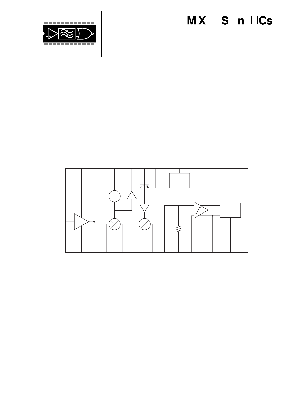
The CMX018 is a single chip UHF FM/FSK double-conversion super-heterodyne receiver. It combines a dual
gain mode Low Noise Amplifier (LNA), two down-converters (including integrated oscillators), limiting
amplifier, RSSI, FM/FSK demodulator and zero-power mode control.
The CMX018 can be used in conjunction with the CMX017, an integrated FM/FSK modulator and transmitter,
to implement a complete UHF radio link.
The CMX018 operates from a 2.7V to 3.3V power supply and is available in the following package style:
28-pin SSOP (CMX018D6).
1999 MX-COM, Inc. www.mxcom.com Tel: 800 638 5577 336 744 5050 Fax: 336 744 5054 Doc. # 20480194.003
4800 Bethania Station Road, Winston-Salem, NC 27105-1201 USA All trademarks and service marks are held by their respective companies.
Page 2

UHF FM/FSK Receiver 2 CMX018 Advance Information
CONTENTS
Section Page
1 Internal Block Diagram..................................................................................................3
2 Signal List.......................................................................................................................4
3 External Components....................................................................................................5
4 General Description.......................................................................................................6
4.1 Low Noise Amplifier............................................................................................................. 6
4.2 First Down-Converter .......................................................................................................... 6
4.3 Second Down-Converter ..................................................................................................... 6
4.4 Limiting Amplifier and RSSI................................................................................................. 6
4.5 FM/FSK Demodulator.......................................................................................................... 6
4.6 Zero-Power Mode................................................................................................................ 6
5 Application Notes ..........................................................................................................7
5.1 General................................................................................................................................ 7
6 Performance Specification..........................................................................................10
6.1 Electrical Performance ...................................................................................................... 10
6.1.1 Absolute Maximum Ratings.................................................................................................. 10
6.1.2 Operating Limits...................................................................................................................10
6.1.3 Operating Characteristics.....................................................................................................11
6.2 Packaging.......................................................................................................................... 13
6.3 Handling Precautions ........................................................................................................ 13
MX-COM, Inc. reserves the right to change specifications at any time and without change.
1999 MX-COM, Inc. www.mxcom.com Tel: 800 638 5577 336 744 5050 Fax: 336 744 5054 Doc. # 20480194.003
4800 Bethania Station Road, Winston-Salem, NC 27105-1201 USA All trademarks and service marks are held by their respective companies.
Page 3
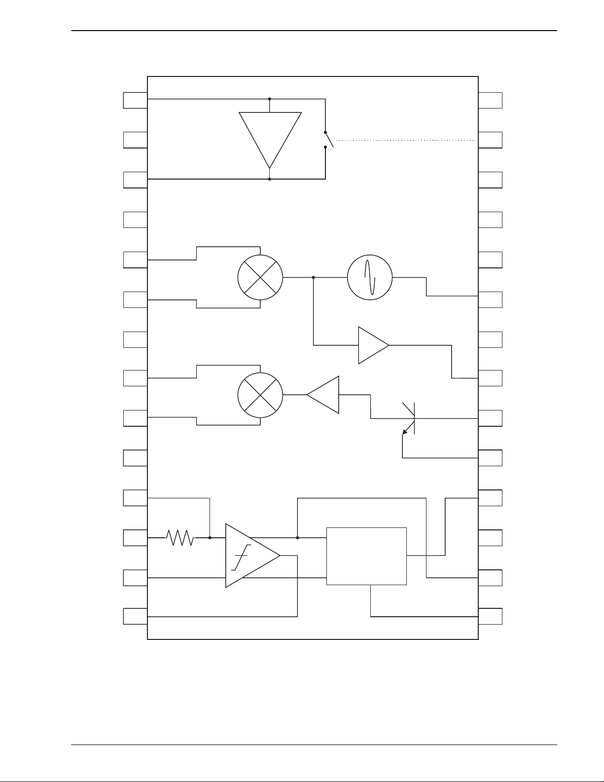
UHF FM/FSK Receiver 3 CMX018 Advance Information
1
Internal Block Diagram
LNAIN
GND
LNAOUT
GND
MIX1IN
MIX1OUT
GND
MIX2IN
1
28
ENABLE
LNA
27
26
25
24
23
22
GAINSEL
LNADEC
V 1
CC
GND
TANK
V 2
CC
2
3
4
ST
1DOWN
5
CONVERTER
6
7
BUFFERED
VCO OUTPUT
21
8
OSCOUT
MIX2OUT
GND
LIMIN
LIMDEC1
LIMDEC2
RSSI
10
11
12
13
14
20
9
ND
2DOWN
OSCBA
CONVERTER
19
OSCEM
18
IF LIMITING
DETOUT
AMPLIFIER
430W
17
V 3
CC
FM/FSK
DEMODULATOR
16
LIMOUT
15
QUADIN
Figure 1: Internal Block Diagram
1999 MX-COM, Inc. www.mxcom.com Tel: 800 638 5577 336 744 5050 Fax: 336 744 5054 Doc. # 20480194.003
4800 Bethania Station Road, Winston-Salem, NC 27105-1201 USA All trademarks and service marks are held by their respective companies.
Page 4
UHF FM/FSK Receiver 4 CMX018 Advance Information
2 Signal List
Pin No. Signal
Description
Package D6 Name Type
1 LNAIN input LNA RF Input
2 GND ground LNA Ground connection
3 LNAOUT output LNA RF Output
4 GND ground LNA Ground connection
5 MIX1IN input RF Input to the First Down-Converter
6 MIX1OUT output IF Output from the First Down-Converter
7 GND ground First Down-Converter Ground connection
8 MIX2IN input RF Input to the Second Down-Converter
9 MIX2OUT output IF Output from the Second Down-Converter
10 GND ground Second Down-Converter, Limiting Amplifier, RSSI, and
Demodulator stages - Ground connection
11 LIMIN input Input to the Limiting Amplifier
12 LIMDEC1 input
13 LIMDEC2 input
External Decoupling capacitors – one required at each limiting
Amplifier Inputs
14 RSSI output Receive Signal Strength Indicator output
15 QUADIN input Quadrature input to the FM Demodulator
16 LIMOUT output Output from the Limiting Amplifier
17 Vcc3 power Power supply to the Second Down-Converter, Limiting Amplifier,
RSSI and Demodulator stages – nominally 3.0V
18 DETOUT output Output of the FM/FSK Quadrature Demodulator
19 OSCEM
Emitter connection to the Second Down-Converter Local Oscillator
transistor
20 OSCBA Base connection to the Second Down-Converter Local Oscillator
transistor
21 OSCOUT output
Buffered Local Oscillator (Open-Collector) output from the First
Down-Converter
22 VCC2 power First Down-Converter 3V Supply
23 TANK input
First Down-Converter Local Oscillator (VCO) TANK/Resonator
connection
24 GND ground First Down-Converter VCO Ground connection
25 VCC1 power LNA Power Supply – nominally 3.0V
26 LNADEC External LNA bias decoupling capacitor
27 GAINSEL CMOS input LNA Gain control logic input. A logic ‘0’ provides a typical power
gain of 16dB and a logic ‘1’ provides an attenuation of 6dB
28 ENABLE CMOS input Zero-Power logic control. A logic ‘0’ powers down the device.
Table 1: Signal List
1999 MX-COM, Inc. www.mxcom.com Tel: 800 638 5577 336 744 5050 Fax: 336 744 5054 Doc. # 20480194.003
4800 Bethania Station Road, Winston-Salem, NC 27105-1201 USA All trademarks and service marks are held by their respective companies.
Page 5

UHF FM/FSK Receiver 5 CMX018 Advance Information
3 External Components
3V
FSK Modulated RF
Input Signal
RSSI Outout
BPF
CF = 915MHz
BPF
CF = 915MHz
BPF
CF = 70.875MHz
BPF
CF = 10.7MHz
0V
Dis
LNAIN
1
GND
2
LNAOUT
3
GND
4
MIX1IN
5
MIX1OUT
6
GND
7
MIX2IN
MIX2OUT
GND
LIMIN
C1
LIMDEC1
LIMDEC2
C2
RSSI
CMX018D6
8
9
10
11
12
13
14
28
27
26
25
24
23
22
21
20
19
18
17
16
15
ENABLE
GAINSEL
LNADEC
V
CC1
GND
TAN K
V
CC2
OSCOUT
OSCBA
OSCEM
DETOUT
V
CC3
LIMOUT
QUADIN
C6
EnLoHi
C13
3V
0V
C15
C14
3V
C
DEC
C
DEC
L1
L2
C
RESONAT OR
C11 C12
3V
DEC
L3
To Audio Amplifier/DataBit Slicer
R1
VCO control from PLL
D1
C9
C7
R2
RF to PLL
C10
60.174MHz
50ppm
C8
R3
=750mV/kHz;
C4
C5
L4
100pF
C
DEC
=
10nF
1Fm
DISCRIMINATORSENSITIVITY
C3
measured at DETOUT(pin 18)
Figure 2: Example of CMX018 with External Components
C1 100nF C15 100pF
C2 100nF D1 Varactor Varactor diode, type SMV1233-011
C3 100nF ~ Resonator Co-Axial Resonator, type RG402, length = 11mm, shorted end
C4 200pF L1 22nH
C5 8 – 50pF
L2 680nH
Trimmer
C6 5pF L3 680nH
C7 220pF L4
C8 6.8pF R1
C9 15pF R2
C10 33pF R3
1µH
10k
10k
2.0k
Ω
Ω
Ω
Value is application dependent
C11 4.7pF
C12 6.2pF X1 60.175MHz 50ppm crystal
C13 10nF
C14 100pF
Note: Components are surface mount, type SMD0603, unless otherwise indicated.
Table 2: Example of CMX018 with External Components
1999 MX-COM, Inc. www.mxcom.com Tel: 800 638 5577 336 744 5050 Fax: 336 744 5054 Doc. # 20480194.003
4800 Bethania Station Road, Winston-Salem, NC 27105-1201 USA All trademarks and service marks are held by their respective companies.
Page 6

UHF FM/FSK Receiver 6 CMX018 Advance Information
4 General Description
The CMX018 is a single chip UHF FM/FSK double-conversion super-heterodyne receiver. It combines a dual
gain mode Low Noise Amplifier (LNA), two down-converters (including integrated oscillators), limiting
amplifier, RSSI, FM/FSK demodulator and zero-power mode control.
The receiver frequency is selected using an external PLL or synthesizer, which is driven by the buffered RF
oscillator signal from the first down-converter.
The CMX018 can be used in conjunction with the CMX017, an integrated FM/FSK modulator and transmitter,
to implement a complete UHF radio link.
4.1 Low Noise Amplifier
The LNA includes a switched gain function, which is used to increase the dynamic range of the receiver. The
gain is selected using the GAINSEL logic input at pin 2. With a logic ‘0’ at the GAINSEL input a high gain is
selected and the amplifier achieves the lowest noise figure. This mode is used where maximum sensitivity is
required for low level input signals. Where high level signals are present at the receiver input, which cause
difficulties due to inter-modulation, the gain of the LNA can be reduced by typically 22dB from about +16dB to
about –6dB. The attenuation is selected by applying a logic ‘1’ at the GAINSEL input; this minimizes the
amount of non-linear distortion in the overall receiver at the expense of small signal sensitivity. The input and
output impedances of the LNA are typically 50Ω.
4.2 First Down-Converter
The first down-converter includes a double balanced mixer with a low noise pre-amplifier, and on-chip
oscillator components. The oscillator is configured as a ‘high-sided’ voltage controlled local oscillator, using
an external varicap diode and tank resonator circuit, such that the first IF is typically centered at 70MHz. A
buffered oscillator signal (OSCOUT at pin 21) is provided to drive the frequency synthesizer which controls
the frequency tuning. The input impedance is typically 50Ω and the output impedance is typically 100Ω.
4.3 Second Down-Converter
The second down-converter also includes a double balanced mixer with a low noise pre-amplifier, and on-chip
oscillator components. The oscillator is configured as a ‘low-sided’ local oscillator, using an external crystal at
typically 60MHz, such that the second IF is centered at 10.7MHz. The input impedance is typically 100Ω and
the output impedance is typically 430Ω.
4.4 Limiting Amplifier and RSSI
The limiting amplifier provides the IF amplification and limiting prior to the FM/FSK demodulator. An RSSI
circuit is included which has temperature compensation. An RF signal level of -100dBm at the LNA input will
produce an RSSI voltage of typically TBD mV. The RSSI voltage will increase with increasing RF input level
at a rate of 20mV/dB up to a typical voltage of TBD V at a -60dBm RF input. In practice the absolute RSSI
voltage will depend upon the insertion losses associated with each of the IF filters. The input impedance is
typically 430Ω.
4.5 FM/FSK Demodulator
A quadrature detector is employed together with an external discriminator and phase shift network to
demodulate the FM or FSK signal.
4.6 Zero-Power Mode
The device is powered down by applying a logic ‘0’ level at the ENABLE input (pin 28). In this mode the
device current is reduced to less than 10µA. This feature is useful when the device is operating within a
transceiver where the receiver needs to be enabled and disabled.
A delay should be allowed for the receiver to settle after power-up. This is likely to be less that the crystal
oscillator stabilization time, which may be altered by adjusting the value of R2, shown in Figure application.
1999 MX-COM, Inc. www.mxcom.com Tel: 800 638 5577 336 744 5050 Fax: 336 744 5054 Doc. # 20480194.003
4800 Bethania Station Road, Winston-Salem, NC 27105-1201 USA All trademarks and service marks are held by their respective companies.
Page 7

UHF FM/FSK Receiver 7 CMX018 Advance Information
5 Application Notes
5.1 General
Example Schematic and Layout
The following schematic (Figure 3) and printed circuit layout (Figure 4 and Figure 5) show a typical application
interface for the CMX018. To aid legibility, the schematic and layout are available electronically from the MXCOM website http://www.mxcom.com.
Alternative components and component values are shown on the schematic. These should be selected
according to the intended application. The schematic uses the following ICs:
U2 Motorola MC34072D-SO8
U3 IC Works WB1315X
U4 Analog Devices AD8532-SO8
1999 MX-COM, Inc. www.mxcom.com Tel: 800 638 5577 336 744 5050 Fax: 336 744 5054 Doc. # 20480194.003
4800 Bethania Station Road, Winston-Salem, NC 27105-1201 USA All trademarks and service marks are held by their respective companies.
Page 8

UHF FM/FSK Receiver 8 CMX018 Advance Information
R16
100R
C93
C4
C2
RFIN
J2
C12
C9
N/C
N/C
33pF
3V
C24
C17
N/C
C8
N/C
5
FLT1
2
F5CH-915M-L2
SAW FILTER
OUT
IN
100pF
100pF
100pF
GND
GND
GND
GND
10nF
C47
10k
R15
N/C-3pF
C46
D1
C44
10pF
2
IN
1
GND
RXRESNR
C43
100nF
R14
100nF
100nF
C37
10k-N/C
1nF
4.7pF
C63
1nF
C45
33pF
C56
15pF
C57
L7
680nH
C69
10nF
C33
C320
1nF
1uF
L16
L15
L14
28
1
N/C
ENABLE
LNAIN
27
GAINSEL
GND1
2
C28
1nF
C36
26
25
24
23
22
21
20
TANK
VCC1
VCC2
LNADEC
OSCOUT
OSCGND
U4
CMX018D6
LNAOUT
GND2
MIX1IN
MIX1OUT
GND3
MIX2IN
3
4
5
6
7
8
9
C55
C35
100pF
C34
100pF
19
OSCBA
MIX2OUT
10
OSCEM
GND4
1nF
C68
18
17
16
15
VCC3
LIMOUT
QUADIN
DETOUT
LIMIN
LIMDEC1
LIMDEC2
RSSI
11
12
13
14
100nF
C66
100nF
C65
1nF
C60
3
3
2
OUT
1
GND
IN
1
U5
KMFC545S
N/C
C27
C38
100pF
6
4
3
1
C21
N/C
2
FLT2
5
F5CH-915M-L2
SAW FILTER
IN
OUT
C30
GND
1
GND
3
GND
4
GND
6
100pF
C31
L6
C54
C42
12.5nH
360pF
C41
N/C
33pF
L5
8nH
C52
C26
C40
33pF
L4
C50
12.5nH
C39
N/C
360pF
C64
C62
5pF
XT1
OUT
IN
N/C
180pF
330pF
180pF
6.8pF
GND
C53
C51
C49
220pF
C72
R22
2
U6
R1
HC49U-S
R18
C73
L10
KMFC545P
0R-N/C
L9
L8
CV1206
200pF
2k
1uH
C77
120pF
120+27pF
120pF
C1
L1
N/C
10k-N/C
680nH
5V
100nF
15uH
C3
1nF
7
( -NC)
2.2uF
1
6
AD8532-SO8
R6
8
+
U1
3
R3
N/C
0R
5
4
-
2
R7
R8
C18
47K - N/C
1k
470nF
C19
100nF
100pF
C20
L3
22nH
3V
C29
100pF
2.2uF
C16
100pF
C15
100nF
C14
5V
15uH
L2
C23
100pF
20
19
18
17
16
15
14
13
12
11
VP2
VCC2
VCC1
VP1
1
2
LE
DO2
GND
GND
FIN2
DATA
FIN2B
CLOCK
U3
WB1315X
SYNT_STB
SYNT_CLK
DO1
GND
FIN1
FIN1B
GND
OSC_IN
3
GND
4
5
6
7
8
9
10
FO_LD
SYNT_DATA
100pF
C13
C61
2k2
N/C
R47
R10
2
J1
1
100pF
C58
100pF
C59
100pF
C48
C22
100pF
1nF
C25
100pF
100pF
C460
100pF
1uF
C67
4
6
3
5
R100
C81
3V
5V
L11
100pF
820nH
C470
100nF
8
10
12
14
16
7
9
11
13
15
100
100pF
C10
10nF
C87
C80
18
20
100nF
C79
17
19
TFMCON20M
100uF
C78
7
R4
6p8
C71
100k
+
-
6
5
100k
R9
R2
10k
R5
100k
C7
C6
C5
1nF
1nF
C70
2.2uF
U2
4
-
2
2.2uF
C32
47nF
1nF
C11
1
MC34072D
8
+
3
5V
Figure 3: Application Schematic
1999 MX-COM, Inc. www.mxcom.com Tel: 800 638 5577 336 744 5050 Fax: 336 744 5054 Doc. # 20480194.003
4800 Bethania Station Road, Winston-Salem, NC 27105-1201 USA All trademarks and service marks are held by their respective companies.
Page 9

UHF FM/FSK Receiver 9 CMX018 Advance Information
Figure 4: Application Layout - Top Copper
Figure 5: Application Layout - Bottom Copper (not reversed)
Available from http://www.mxcom.com.
1999 MX-COM, Inc. www.mxcom.com Tel: 800 638 5577 336 744 5050 Fax: 336 744 5054 Doc. # 20480194.003
4800 Bethania Station Road, Winston-Salem, NC 27105-1201 USA All trademarks and service marks are held by their respective companies.
Page 10

UHF FM/FSK Receiver 10 CMX018 Advance Information
6 Performance Specification
6.1 Electrical Performance
6.1.1 Absolute Maximum Ratings
Exceeding these maximum ratings can result in damage to the device.
Pins Min. Max. Units
Supply Voltage (VCC) 17, 22, 25 -0.3 7.0 V
Input Voltage 27, 28 -0.3 V
LNA Input Power 1 0 dBm
D6 Package
Total Allowable Power Dissipation at T
= 25°C 550 mW
AMB
Derating above 25°C
Storage Temperature -55 +125 °C
6.1.2 Operating Limits
Correct operation of the device outside these limits is not implied.
Notes Min. Max. Units
Supply Voltage (VCC)2.73.3V
RF Input Range 860 965 MHz
Operating Temperature -10 +60 °C
+ 0.3 V
CC
9
mW/°C above 25°C
1999 MX-COM, Inc. www.mxcom.com Tel: 800 638 5577 336 744 5050 Fax: 336 744 5054 Doc. # 20480194.003
4800 Bethania Station Road, Winston-Salem, NC 27105-1201 USA All trademarks and service marks are held by their respective companies.
Page 11

UHF FM/FSK Receiver 11 CMX018 Advance Information
6.1.3 Operating Characteristics
For the following conditions unless otherwise specified:
V
= 2.7V to 3.3V, T
CC
= - 10°C to +60°C,
AMB
RF = 915MHz, 50Ω source and load impedance.
Pin Note Min. Typ. Max. Units
DC Parameters
ICC (ENABLE = VCC and GAINSEL = 0V) 17, 22, 25 50 mA
ICC (ENABLE = VCC and GAINSEL = VCC) 17, 22, 25 42 mA
ICC (ENABLE = 0V) 17, 22, 25 10
AC Parameters
LNA (RF = 915MHz)
Power Gain (GAINSEL = 0V) 1, 3 16 dB
Power Gain (GAINSEL = VCC) 1, 3 -6.0 dB
Noise Figure 1, 3 3.0 dB
Input 1dB Gain Compression Point (GAINSEL = 0V) 1 -20 dBm
Input 1dB Gain Compression Point (GAINSEL = VCC) 1 16 dBm
Input Third Order Intercept Point (GAINSEL = 0V) 1 -10 dBm
Input Third Order Intercept Point (GAINSEL= VCC) 1 25 dBm
Reverse Isolation (GAINSEL = 0V) 3, 1 -35 dB
Reverse Isolation (GAINSEL = VCC) 3, 1 -6.0 dB
Input Impedance 1 50
Output Impedance 3 50
Input Return Loss (50Ω source)
Output Return Loss (50Ω load)
1
3
10
15
VCO to LNA Leakage 1 -45 dBm
First Down Converter
(RF = 915MHz and IF = 70MHz)
Conversion Gain 5, 6 15 dB
Noise Figure 5, 6 15 dB
Input 1dB Gain Compression Point 6 -12 dBm
Input Third Order Intercept Point 6 -4.0 dBm
Input Impedance 5 50
Output Impedance 6 100
Input Return Loss (50Ω source)
Output Return Loss (50Ω load)
5TBDdB
6TBDdB
Buffered oscillator output power 21 -10 dBm
RF to IF Leakage 5, 6 TBD dB
LO to IF Leakage 6 TBD dBm
LO to RF Leakage 5 TBD dBm
µ
Ω
Ω
dB
dB
Ω
Ω
A
1999 MX-COM, Inc. www.mxcom.com Tel: 800 638 5577 336 744 5050 Fax: 336 744 5054 Doc. # 20480194.003
4800 Bethania Station Road, Winston-Salem, NC 27105-1201 USA All trademarks and service marks are held by their respective companies.
Page 12

UHF FM/FSK Receiver 12 CMX018 Advance Information
Pin Note Min. Typ. Max. Units
Second Down Converter
(RF = 70MHz and IF = 10.7MHz)
Conversion Gain 8, 9 24 dB
Noise Figure 8, 9 13 dB
Output 1dB Gain Compression Point 9 -11 dBm
Output Third Order Intercept Point 9 -2 dBm
Input Impedance 8 100
Output Impedance 9 430
Ω
Ω
Limiting Amplifier and RSSI
(IF = 10.7MHz)
Bandwidth 11, 16 40 MHz
Internal Voltage Gain 11 74 dBV
Input Impedance 11 430
RSSI Dynamic Range 14
RSSI Slope 14
RSSI Voltage Range 14 1
TBD
TBD
TBD
Ω
dB
V/dB
V
Demodulator (IF = 10.7MHz)
Output Swing 18 2
TBD
Output Impedance 18 1
MV
k
P-P
Ω
Notes:
1. Input power = TBD to TBD
2. 125kHz Deviation, 1kΩ Load
1999 MX-COM, Inc. www.mxcom.com Tel: 800 638 5577 336 744 5050 Fax: 336 744 5054 Doc. # 20480194.003
4800 Bethania Station Road, Winston-Salem, NC 27105-1201 USA All trademarks and service marks are held by their respective companies.
Page 13

UHF FM/FSK Receiver 13 CMX018 Advance Information
6.2 Packaging
Figure 6: 28-Pin Plastic SSOP Mechanical Outline:
Order as part no. CMX018D6
6.3 Handling Precautions
This device is a high performance RF integrated circuit and is ESD sensitive.
Adequate precautions must be taken during handling and assembly of this device.
1999 MX-COM, Inc. www.mxcom.com Tel: 800 638 5577 336 744 5050 Fax: 336 744 5054 Doc. # 20480194.003
4800 Bethania Station Road, Winston-Salem, NC 27105-1201 USA All trademarks and service marks are held by their respective companies.
 Loading...