

Page 1
DATA BULLETIN
CMX017
UHF FM/FSK Transmitter
ADVANCE INFORMATION
Features Applications
•
Direct FM/FSK UHF Modulator
•
Adjustable Modulator Output Power
•
Integrated Power Amplifier with Output
Power up to +20dBm (100mW)
•
Low Power 2.7V Operation
•
Powersave and Zero-Power
(<10µA) Modes
•
28-Pin SSOP Package
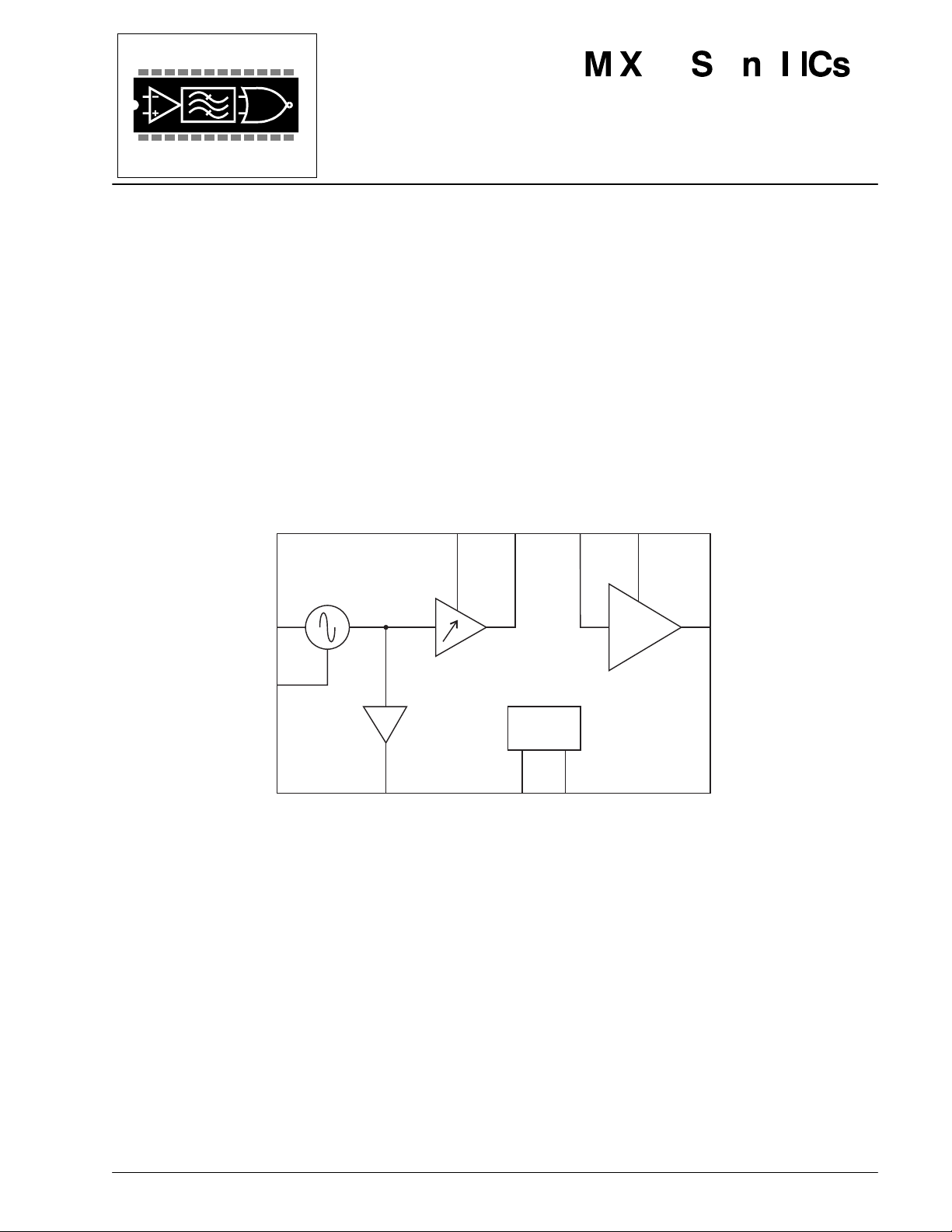
MODIN
FM/FSK
MODULATOR
POWER
AMPLIFIER
DRIVER
GAIN MODOUT PAIN IPAOUT
•
General Radio Link 860-965MHz
•
General 915MHz ISM Band (USA)
•
Spread Spectrum Wireless
Systems
•
Fixed Frequency Transmissions
•
Analog/Digital Cordless Phones
•
Handheld Data Terminals
•
SO-HO Wireless Data Links
POWER
AMPLIFIER
PAOUT
TAN K
BUFFERED
OSCILLATOR
OUTPUT
OSCOUT
The CMX017 is a single chip UHF FM/FSK transmitter that combines both the RF VCO Modulator and RF
Power Amplifier. It is suitable for both audio FM and digital FSK transmissions.
A buffered oscillator output provides the RF signal drive to an external synthesizer or fixed frequency phaselocked loop for channel frequency selection. Modulator output power is adjustable over a 20dB range and the
integrated power amplifier delivers up to +20dBm. The device also includes a powersave mode: “Transmit
Standby” and a zero-power mode: “Sleep”. These allow independent power down control of both the
modulator and power amplifier, thereby maximizing battery life. The device can be used in conjunction with
the CMX018, a double-conversion super-heterodyne receiver, to implement a complete UHF radio link.
The CMX017 operates from a 2.7V to 3.3V power supply and is available in the following package style:
28-pin SSOP (CMX017D6).
BANDGAP & BIAS
CONTROL
ENLMOD
ENLPA
1999 MX-COM, Inc. www.mxcom.com Tel: 800 638 5577 336 744 5050 Fax: 336 744 5054 Doc. # 20480193.003
4800 Bethania Station Road, Winston-Salem, NC 27105-1201 USA All trademarks and service marks are held by their respective companies
Page 2

UHF FM/FSK Transmitter 2 CMX017 Advance Information
CONTENTS
Section Page
1 Block Diagram................................................................................................................3
2 Signal List.......................................................................................................................4
3 External Components....................................................................................................5
4 General Description.......................................................................................................6
4.1 FM/FSK Modulator + PA Driver........................................................................................... 6
4.2 Power Amplifier (PA) ........................................................................................................... 6
4.3 Power-Down Modes ............................................................................................................ 6
5 Application Notes ..........................................................................................................6
5.1 Generation of the Modulated RF Signal .............................................................................. 6
5.2 Power-Down Modes ............................................................................................................ 7
6 Performance Specification..........................................................................................10
6.1 Electrical Performance ...................................................................................................... 10
6.1.1 Absolute Maximum Ratings.................................................................................................. 10
6.1.2 Operating Limits...................................................................................................................10
6.1.3 Operating Characteristics.....................................................................................................10
6.1.4 Packaging.............................................................................................................................12
MX-COM, Inc reserves the right to change specifications at any time and without notice.
1999 MX-COM, Inc. www.mxcom.com Tel: 800 638 5577 336 744 5050 Fax: 336 744 5054 Doc. # 20480193.003
4800 Bethania Station Road, Winston-Salem, NC 27105-1201 USA All trademarks and service marks are held by their respective companies
Page 3
UHF FM/FSK Transmitter 3 CMX017 Advance Information
1 Block Diagram
V3
CC
GAIN
GND
GND
GND
IPAOUT
GND
GND
PAOUT
1
2
P A DRIVER
3
PA
4
ST AGE 1
5
BUFFERED
OSCILLATOR
OUTPUT
6
7
PA
ST AGE 2
8
FM/FSK
MODULATOR
9
28
27
26
25
24
23
22
21
20
PAIN
GND
MODOUT
GND
V2
CC
OSCOUT
V1
CC
GND
TANK
10
GND
11
GND
V4
ENLPA
12
CC
13
PACKAGE
14
GND GND
GROUND
SUBSTRA TE
PACKAGE
GROUND
19
18
17
16
15
Figure 1: Internal Block Diagram
GND
MODIN
GND
ENLMOD
1999 MX-COM, Inc. www.mxcom.com Tel: 800 638 5577 336 744 5050 Fax: 336 744 5054 Doc. # 20480193.003
4800 Bethania Station Road, Winston-Salem, NC 27105-1201 USA All trademarks and service marks are held by their respective companies
Page 4

UHF FM/FSK Transmitter 4 CMX017 Advance Information
2 Signal List
Pin No. Signal
Description
D6 Package Name Type
1V
3 power Power amplifier (first stage) power supply - nominally 3.0V
CC
2 GAIN input Modulator output (pin 26) - Power control
3 GND ground Ground-plane connection to the power amplifier
4 GND ground Ground-plane connection to the power amplifier
5 GND ground Ground-plane connection to the power amplifier
6 IPAOUT output Output (open-collector) from the first stage of the power
amplifier
7 GND ground Ground-plane connection to the power amplifier
8 GND ground Ground-plane connection to the power amplifier
9 PAOUT output
Output (open-collector) from the second stage of the power
amplifier
10 GND ground Ground-plane connection to the power amplifier
11 GND ground Ground-plane connection to the power amplifier
12 VCC4 power Power amplifier (second stage) power supply
– nominally 3.0V
13 ENLPA
CMOS
input
Power Amplifier powersave logic control. A logic “0” powers
down the Power Amplifier and Driver stages
14 GND ground Ground-plane connection
15 GND ground Ground-plane connection
16 ENLMOD CMOS
input
Modulator zero-power logic control. A logic “0” powers down
the Modulator and Buffered Oscillator stages
17 GND ground Ground-plane connection
18 MODIN input Baseband modulation input signal
19 GND ground Ground-plane connection to the VCO
20 TANK input VCO Tank circuit/Resonator connection
21 GND ground Ground-plane connection to the modulator and VCO buffer
22 VCC1 power Modulator power supply – nominally 3.0V
23 OSCOUT output Buffered Oscillator (open-collector) output
24 VCC2 power Power Amplifier Driver power supply - nominally 3.0V
25 GND ground Ground-plane connection for the Power Amplifier Driver
26 MODOUT output Modulator output
27 GND ground Ground-plane connection for the Power Amplifier Driver
28 PAIN input Power Amplifier input
Table 1: Signal List
1999 MX-COM, Inc. www.mxcom.com Tel: 800 638 5577 336 744 5050 Fax: 336 744 5054 Doc. # 20480193.003
4800 Bethania Station Road, Winston-Salem, NC 27105-1201 USA All trademarks and service marks are held by their respective companies
Page 5

UHF FM/FSK Transmitter 5 CMX017 Advance Information
3 External Components
POWER CONTROL
Tx SIGNAL
3V
V
C
DEC
C6
C7
C5
L1
L2
C8
C9
CC3
GAIN
GND
GND
GND
IPAOUT
GND
GND
PAOUT
GND
GND
V
CC4
ENLP A
GND
1
2
3
4
5
6
7
CMX017D6
8
9
10
11
12
13
14
28
27
26
25
24
23
22
21
20
19
18
17
16
15
PAIN
GND
MODOUT
GND
V
CC2
OSCOUT
V
CC1
GND
TANK
GND
MODIN
GND
ENLMOD
GND
L3
C1
RF to PLL
C2
C3
R2
C10
RESONA TOR
C4
R3
D1
R1R1
C11
L4
R4
SMD POT
3V
C
DEC
C12
R1
From PLL
BASE-BAND
ENABLE POWER AMPLIFIER
C
DEC
1Fm
º
100pF10nF
ENABLE MODULATOR
Figure 2: Example of CMX017 with External Components
C1 5.6pF C12 100pF
C2 33pF D1 Varactor Varactor diode, type SMV1233-011
C3 4.3pF ~ Resonator Co-Axial Resonator, type RG402, length = 11mm, shorted end
C4 TBD L1 1.5nH
C5 100pF L2 22nH
C6 100pF L3 6.8nH
C7 100pF L4 22nH
C8 100pF R1
C9 100pF R2
10k
10k
Ω
Ω
C10 100pF R3 TBD Value is application dependent
C11 100pF R4 TBD SMD potentiometer - value is application dependent
Note: Components are surface mount, type SMD0603, unless otherwise indicated.
Figure 3: Example of CMX017 with External Components for 915MHz Operation
1999 MX-COM, Inc. www.mxcom.com Tel: 800 638 5577 336 744 5050 Fax: 336 744 5054 Doc. # 20480193.003
4800 Bethania Station Road, Winston-Salem, NC 27105-1201 USA All trademarks and service marks are held by their respective companies
Page 6

UHF FM/FSK Transmitter 6 CMX017 Advance Information
4 General Description
The CMX017 is a single chip UHF FM/FSK transmitter that combines both the RF VCO Modulator and RF
Power Amplifier. It is suitable for both audio FM and digital FSK transmissions.
A buffered oscillator output provides the RF signal drive to an external synthesizer or fixed frequency phaselocked loop for channel frequency selection. Modulator output power is adjustable over a 20dB range and the
integrated power amplifier delivers up to +20dBm. The device also includes a powersave mode: “Transmit
Standby” and a zero-power mode: “Sleep”. These allow independent power down control of both the
modulator and power amplifier, thereby maximizing battery life. The device can be used in conjunction with
the CMX018 a double-conversion super-heterodyne receiver, to implement a complete UHF radio link.
4.1 FM/FSK Modulator + PA Driver
The modulator circuit uses an integrated oscillator whose frequency can be directly modulated by the DCcoupled input base-band signal, at the MODIN pin, to generate a frequency modulated (FM or FSK) RF
signal. The oscillator requires an external varactor and resonator circuit, connected at the TANK pin, to tune
to the required RF channel. A buffered oscillator signal is provided from an open-collector output, at the
OSCOUT pin, to drive an external frequency synthesizer for the channel selection.
The output power, at the MODOUT pin, is variable over a 20dB range. The output power is maximum when
the GAIN pin is connected to V
output impedance at the MODOUT pin is typically 50Ω.
4.2 Power Amplifier (PA)
The power amplifier has two internal stages, each biased for class-B operation, and is designed to have a
fixed overall power gain. The input and output impedances can be terminated with 50Ω. A typical power gain
improvement of 2dB is achieved using simple external matching networks.
and is reduced by typically 20dB when this pin is connected to 0V. The
CC
4.3 Powersave and Zero-Power Modes
The Modulator and Buffered Oscillator stages are powered down independently of the PA Driver + Power
Amplifier stages by means of the ENLMOD and ENLPA logic inputs:
A logic ‘0’ at ENLMOD powers down the Modulator and Buffered Oscillator stages.
A logic ‘0’ at ENLPA powers down the PA Driver and Power Amplifier stages.
Refer to the block diagram in Figure 1 and to Section 5.
5 Application Notes
5.1 Generation of the Modulated RF Signal
The modulator on the CMX017 relies on the direct modulation of the RF Voltage Controlled Oscillator (VCO),
which is stabilized to the channel center frequency by an external Frequency Synthesizer or Phase Locked
Loop (PLL). The user has control over the external PLL filter and VCO tank components and choice of these
components will have an impact upon the following PLL parameters:-
Closed loop bandwidth, settling time and transient response
Modulation linearity
VCO phase noise
Three modulation requirements may be achieved as follows:
5.1.1 The minimum modulation signal frequency is above the PLL Closed Loop Bandwidth
In applications where the transmit channel frequency is fixed or occasionally changed, a narrow PLL
bandwidth can be chosen such that the minimum modulation frequency is in excess of the PLL bandwidth.
With the PLL active whilst the base-band signal is applied to the modulator there will be negligible distortion of
the modulated RF output signal. A benefit of this technique is that an output phase noise improvement is
achieved, compared to the free running VCO phase noise characteristic.
5.1.2 The minimum modulation signal frequency is within the PLL Closed Loop Bandwidth
In Frequency Hopped Spread Spectrum applications the frequency synthesizer must be agile. Consequently
the PLL bandwidth should be designed to achieve the required hop-rate and, in most systems this bandwidth
will exceed the minimum modulation frequency. With the PLL active during modulation, the loop will
1999 MX-COM, Inc. www.mxcom.com Tel: 800 638 5577 336 744 5050 Fax: 336 744 5054 Doc. # 20480193.003
4800 Bethania Station Road, Winston-Salem, NC 27105-1201 USA All trademarks and service marks are held by their respective companies
Page 7

UHF FM/FSK Transmitter 7 CMX017 Advance Information
compensate for the signal frequency components within the loop bandwidth, introducing a frequency
dependant distortion of the modulated RF output signal.
To avoid the modulation distortion the carrier frequency is tuned by the external synthesizer chip, with no
modulating signal applied. The synthesizer control is then disabled, by setting the charge-pump output of the
synthesizer to tri-state. The DC coupled base-band signal, applied to the MODIN pin, then modulates the free
running VCO to generate the FM or FSK output signal.
5.1.3 A flat modulator response is required down to DC, whilst benefiting from the phase noise
improvements due to the PLL (Two-Point Modulation).
Unlike in the above two cases, where a fixed reference frequency is used in the PLL, the Two-Point
Modulation technique requires modulation inputs to both the PLL reference oscillator and to the RF VCO
circuits.
The modulation signal should be applied to both modulation inputs with suitable AC/DC levels and with the
correct phase to achieve cancellation of the loop’s feedback. This prevents the radio’s PLL circuitry from
counteracting the modulation process and so provides a clean flat modulation response down to DC.
5.2 Powersave and Zero-Power Modes
It is possible to power down each section of the transmitter independently. This feature may be useful when
the CMX017 is configured, with the CMX018, as a radio transceiver. It allows the transmitter to be powered
on and off, thereby saving power, during the sleep and standby periods.
In SLEEP mode (ENLMOD=’0’ and ENLPA=’0’) all sections of the device are powered down and the current
consumption is reduced to less than 10µA. This is the zero-power mode.
In TRANSMIT-STANDBY mode (ENLMOD=’1’ and ENLPA=’0’) only the PA Driver and Power Amplifier
stages are powered down, while the Modulator and Buffered Oscillator remain active. This powersave mode
allows the external frequency synthesizer to stabilize the channel center frequency prior to the RF
transmission.
In TRANSMIT mode (ENLMOD=’1’ and ENLPA=’1’) both the Modulator and the Power Amplifier sections of
the device are fully operational.
Note: The device can be used as a stand alone “UHF Power Amplifier” by forcing (ENLMOD=’0’ and
ENLPA=’1’). The efficiency is maximized by connecting the V
connected to 3.0V.)
2 pin to 0V. (The VCC1 pin must remain
CC
5.3 Lower Output Power Applications
For very short range applications the antenna drive can be taken from the modulator output, MODOUT, at
pin 26. The Power Amplifier is powered down by connecting V
3 and VCC4 (pins 1 and 12) to 0V. This
CC
allows the supply current to be minimized and the Modulator output to be enabled or disabled using the
ENLPA input at pin 13.
5.4 Example Schematic and Layout
The following schematic (Figure 4) and printed circuit layout (Figure 5 and Figure 6) present a typical
application interface for the CMX017. To aid legibility, the schematic and layout are available electronically
from the MX-COM website http://www.mxcom.com.
Alternative components and component values are shown on the schematic. These should be selected
according to the intended application. The schematic uses the following ICs:
U2 IC Works WB1315X
U4 Analog Devices AD8532-SO8
1999 MX-COM, Inc. www.mxcom.com Tel: 800 638 5577 336 744 5050 Fax: 336 744 5054 Doc. # 20480193.003
4800 Bethania Station Road, Winston-Salem, NC 27105-1201 USA All trademarks and service marks are held by their respective companies
Page 8

UHF FM/FSK Transmitter 8 CMX017 Advance Information
R2
100R
10nF
C9
R1
10k
3pF
C8
D1
C14
6.8pF
TXRESNR
IN
GND
2
1
1nF
C24
N/C
R9
C27
0R
N/C
L7
15uH
R13
5V
3V
C13
C11
100pF
23
OSCOUT
IPAOUT
6
22
7
100pF
21
20
TANK
VCC1
GND1
CMX017D6
GND7
GND8
PAOUT
8
9
4.7pF
C26
19
OSCGND
GND9
10
C18
100pF
3V
L6
100pF
R14
10K
18
17
16
15
GND
GND
MODIN
ENLMOD
GND10
VCC4
ENLPA
GND
11
12
13
14
20nH
L3
100nH
100nF
C6
N/C
L2
6.8nH
C1
C2
5.6pF
33pF
C7
28
27
26
25
24
PAIN
VCC2
GND3
GND2
MODOUT
U1
VCC3
GAIN
GND4
GND5
GND6
1
2
3
4
5
100pF
C3
L4
1.5nH
C10
100pF
L5
100pF
C5
100uF
C4
100pF
C12
22nH
C15
N/C
12pF
100pF
C16
C65
L1
100nH
33pF
C19
3V
J2
2.2uF
AD8532-SO8
8
U4
47k
5V
7
( - N/C)
1
6
+
-
3
2
0R
R18
5
4
R17
1k
R19
C36
100nF
C35
470nF
N/C
47k
100pF
C22
C37
100pF
19
18
17
16
15
14
13
12
11
GND
GND
4
FIN2
FIN2B
WB1315X
FIN1
FIN1B
5
6
LE
GND
DATA
CLOCK
SYNT_STB
SYNT_CLK
GND
OSC_IN
GND
FO_LD
7
8
9
10
SYNT_DATA
VP2
DO2
VCC2
U2
VCC1
VP1
DO1
2
3
100k
NF
R23
100k
NF
R22
100k
NF
R21
C34
C33
C32
L8
2.2uF
100pF
100nF
15uH
20
1
100pF
C46
C38
1nF
100pF
5V
C31
C42
C44
100pF
C145
100pF
100pF
10nF
C58
18
20
100nF
C57
17
19
TFMCON20M
100uF
C56
L9
15uH
C41
100pF
C39
J1
2
1
100pF
4
6
8
10
12
14
16
3
5
7
9
11
13
15
100
R100
C45
100uF
3V
100pF
100pF
C40
C48
C43
1uF
Figure 4: Application Schematic
1999 MX-COM, Inc. www.mxcom.com Tel: 800 638 5577 336 744 5050 Fax: 336 744 5054 Doc. # 20480193.003
4800 Bethania Station Road, Winston-Salem, NC 27105-1201 USA All trademarks and service marks are held by their respective companies
Page 9

UHF FM/FSK Transmitter 9 CMX017 Advance Information
Figure 5: Application Layout - Top Copper
Figure 6: Application Layout - Bottom Copper (not reversed)
Available from http://www.mxcom.com.
1999 MX-COM, Inc. www.mxcom.com Tel: 800 638 5577 336 744 5050 Fax: 336 744 5054 Doc. # 20480193.003
4800 Bethania Station Road, Winston-Salem, NC 27105-1201 USA All trademarks and service marks are held by their respective companies
Page 10

UHF FM/FSK Transmitter 10 CMX017 Advance Information
6 Performance Specification
6.1 Electrical Performance
6.1.1 Absolute Maximum Ratings
Exceeding these maximum ratings can result in damage to the device.
Pin Min. Max. Units
Supply (VCC) 1, 12, 22,24-0.3 7.0 V
Input Voltage 2, 13, 16,
-0.3 VCC + 0.3 V
18, 20
Power Amplifier Input Power 28 +7 dBm
D6 Package
Total Allowable Power Dissipation at T
= 25°C 1100 mW
AMB
Derating above 25°C 11 mW/°C above 25°C
Storage Temperature -55 +125 °C
Table 2: Absolute Maximum Ratings
6.1.2 Operating Limits
Correct operation of the device outside these limits is not implied.
Notes Min. Max. Units
Supply (VCC)2.73.3V
Operating Frequency Range 860 965 MHz
Operating Temperature -10 +60 °C
Table 3: Operating Limits
6.1.3 Operating Characteristics
For the following conditions unless otherwise specified:
V
= 2.7V to 3.3V, T
CC
= -10°C to +60°C,
AMB
RF = 915MHz, 50Ω source and load impedance.
Pin Note Min. Typ. Max. Units
DC Parameters
Device Fully Enabled
(ENLPA=HI and ENLMOD=HI)
ICC [Output Power = +20dBm at PAOUT (pin 9)] 1 - 130 - mA
ICC [Output Power = +10dBm at PAOUT (pin 9)] 1 - 60 - mA
ICC [Output Power = +0dBm at PAOUT (pin 9)] 1 - 40 - mA
Device in Power-Down Modes
I
in STANDBY mode
CC
ICC in SLEEP Mode
1999 MX-COM, Inc. www.mxcom.com Tel: 800 638 5577 336 744 5050 Fax: 336 744 5054 Doc. # 20480193.003
4800 Bethania Station Road, Winston-Salem, NC 27105-1201 USA All trademarks and service marks are held by their respective companies
(ENLPA=LO and ENLMOD=HI)
(ENLPA=LO and ENLMOD=LO)
1-24-mA
1-TBD10
µ
A
Page 11

UHF FM/FSK Transmitter 11 CMX017 Advance Information
Pin Note Min. Typ. Max. Units
AC Parameters
Modulator, VCO Buffer and PA Driver
Output Power [GAIN (pin 2) at VCC]26--4.0-dBm
Output Power [GAIN (pin 2) at 1.5V] 26 - -9.0 - dBm
Output Power [GAIN (pin 2) at 1.0V] 26 - -14 - dBm
Buffered VCO Output at OSCOUT pin 19 2 - -10 - dBm
Oscillator Second Harmonic Output 26 3 - -25 - dBc
Oscillator Third Harmonic Output 26 3 - -35 - dBc
Modulation Sensitivity 18 4 - 0.4 - MHz/V
Maximum Deviation 26 5 - 1.5 - MHz
Input Data Rate 18 - - TBD kBits/S
Output VSWR (at maximum output power) 26 - TBD -
Power Amplifier
Power Gain 28, 9 - 22 - dB
Power Gain (with external matching at VCC = 3.3V) 28, 9 - 24 - dB
Maximum Power Gain Variation 28, 9 6 - 2.0 - dB
Maximum Power Gain Variation (with matching) 28,9 6 - 1.5 - dB
Input 1dB Compression Point 9 - +1.0 - dBm
Input 1dB Compression Point (with matching) 9 - 0 - dBm
Reverse Isolation 9, 28 - -35 - dB
Output VSWR (at maximum output power) 9 - TBD - dB
Notes:
1. Total current from the external 3V power supply.
2. Power measured into a 50Ω load.
3. With external matching.
4. Stepped modulation voltage input from 1.0V to 2.0V.
5. Stepped modulation voltage from 0V to 3.0V.
6. Input Power = -15dBm to -1dBm.
1999 MX-COM, Inc. www.mxcom.com Tel: 800 638 5577 336 744 5050 Fax: 336 744 5054 Doc. # 20480193.003
4800 Bethania Station Road, Winston-Salem, NC 27105-1201 USA All trademarks and service marks are held by their respective companies
Page 12

UHF FM/FSK Transmitter 12 CMX017 Advance Information
6.2 Packaging
Figure 7: 28-Pin Plastic SSOP Mechanical Outline:
Order as part no. CMX017D6
6.3 Handling Precautions
As this device is a high performance RF integrated circuit and is ESD sensitive. Adequate precautions must
be taken during handling and assembly of this device.
1999 MX-COM, Inc. www.mxcom.com Tel: 800 638 5577 336 744 5050 Fax: 336 744 5054 Doc. # 20480193.003
4800 Bethania Station Road, Winston-Salem, NC 27105-1201 USA All trademarks and service marks are held by their respective companies
 Loading...