

Page 1
CALIFORNIA MICRO DEVICES
MICROPOWER RRO Operational Amplifier
CMV1010
Features
• Tiny SOT23-5 Package
• Guaranteed specs at 1.8V, 2.2V, 2.7V, 3V and 5V
• Ver y Low Supply current typically 50µA @ 3V
• Rail-to-Rail Output
• Typical Total Harmonic Distortion of 0.02% at 3V
• 1.0MHz Typical Gain-Bandwidth Product
• 0.5V/µs Typical Slew Rate
Product Description
The CMV1010 is a high performance CMOS operational amplifier available in a small SOT23-5 package.
Operating with very low supply current, it is ideal for
battery operated applications where power, space and
weight are critical.
With 1MHz Gain Bandwidth Product, 0.5V/µs Slew
Rate, and a typical current consumption of only 50µA,
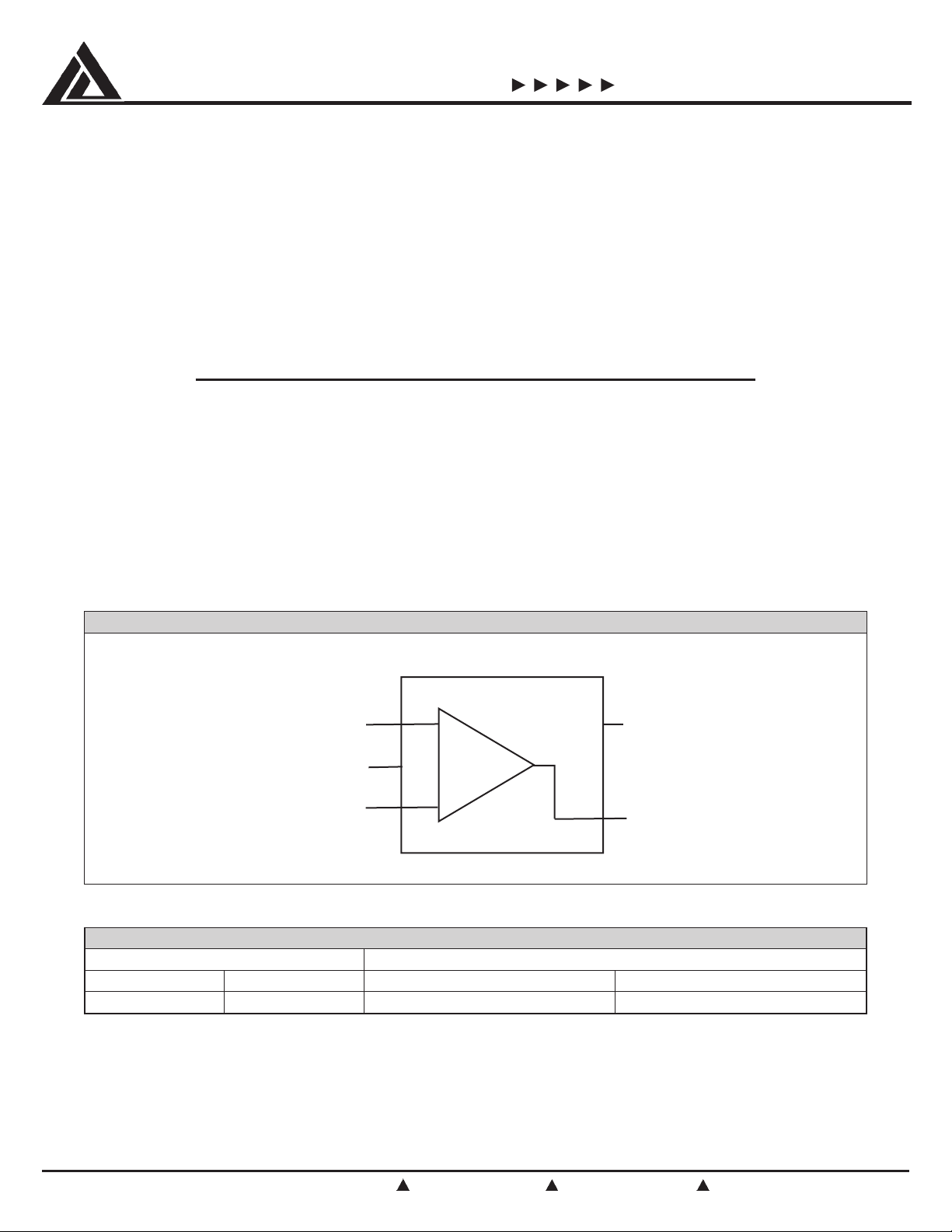
PIN DIAGRAM
Applications
• Mobile Communications
• Cellular Phones
• Portable Equipment
• Notebooks and PDAs
the CMV1010 provides excellent power-performance
ratio for power sensitive applications.
Ideal for use in personal electronics such as cellular
handsets, pagers, cordless telephones and other
products with limited space and battery power.
5-Pin SOT23-5
NON-INV INPUT
V-
INV INPUT
1
2
3
+
-
5
V+
4
OUTPUT
NOITAMROFNIGNIREDROTRAPDRADNATS
egakcaP rebmuNtraPgniredrO
sniPelytSleeR&epaTgnikraMtraP
55-32TOSR/Y0101VMC0101
© 2000 California Micro Devices Corp. All rights reserved.
5/00
215 Topaz Street, Milpitas, California 95035 Tel: (408) 263-3214 Fax: (408) 263-7846 www.calmicro.com
C0920500
1
Page 2
CALIFORNIA MICRO DEVICES
CMV1010
)1ETON(SGNITARMUMIXAMETULOSBA
retemaraPgnitaRtinU
)2etoN,MBH(noitcetorPDSE0002V
egatloVtupnIlaitnereffiD/+−egatloVylppuSV
niPtuptuo/tupnitaegatloVV(,3.0+)+V(−)−3.0V
egarotS:erutarepmeT
)4etoN(noitcnuJgnitarepO
)s01,gniredloS(daeL
−051ot56
521
062
C°
Vot+V(egatloVylppuS−)5.7V
niPtupnItatnerruC5Am
)3etoN(niPtuptuOtatnerruC51Am
sniPylppuSrewoPtatnerruC51Am
)esiwrehtodeificepssselnu(SNOITIDNOCGNITAREPO
retemaraPgnitaRtinU
egatloVylppuS7ot8.1V
erutarepmeTnoitcnuJ
−58ot04
ecnatsiseRlamrehT523W/C°
Note 1: Absolute Maximum Ratings indicate limits beyond which damage to the device may occur. Operating conditions indicate ratings for
Note 2: Human Body Model, 1.5KΩ in series with 100pF.
Note 3: Applies to both single-supply and split-supply operation. Continuous short ckt operation at elevated ambient temperatures can
Note 4: The maximum power dissipation is a function of T
which the device is intended to be functional, but specific performance is not guaranteed. For guaranteed specifications and the
test conditions, see the Electrical Operating Characteristics.
result in exceeding the maximum allowed junction temperature of 150°C.
temperature is P
= (T
D
J (MAX)
- TA)/ θ
. All numbers apply for packages soldered directly to a PC board.
JA
, θJA and TA. The maximum allowable power dissipation at any ambient
J (MAX)
C°
©2000 California Micro Devices Corp. All rights reserved.
2
215 Topaz Street, Milpitas, California 95035 Tel: (408) 263-3214 Fax: (408) 263-7846 www.calmicro.com
5/00
Page 3
CALIFORNIA MICRO DEVICES
CMV1010
SCITSIRETCARAHCGNITAREPOLACIRTCELEV8.1
M1>LR,V0=-V,V8.1=+V,C°52=jTdeificepsesiwrehtosselnU( ΩΩΩΩΩ )
lobmySretemaraPsnoitidnoCpyTtimiLtinU
V
SO
I
B
I
SO
R
NI
I
S
egatloVtesffOtupnIV
tnerruCsaiBtupnI 1Ap
tnerruCtesffOtupnI 5.0Ap
ecnatsiseRtupnI 1TΩ
tnerruCylppuS 0408Aµ
WBGtcudorPhtdiwdnaBniaG 8.0zHM
A
V
RSetaRwelSA
niaGegatloVlangiSegraLV
TUO
=−K001=LR,14.01.0V/sµ
V
RRSPoitaRnoitcejeRylppuSrewoPV2.1ptV9.0=+V
V−=9.0−otV−V2.1
RRMCoitaRnoitcejeRedoMnommoCV8.0<MCV<V00604Bd
V
MC
DHTnoitrotsiDcinomraHlatoTA
I
CS
V
O
egnaRtupnIedoMnommoC 0
=−V,zHK1=f,1
V
tnerruCtiucriCtrohStuptuOkniS/ecruoS5Am
liarrehtiemorfgniwStuptuOK01=LR02051Vm
V9.0=9Vm
TUO
V6.1otV2.0=0806Bd
0705Bd
V0=MCV
1.1
TUO
K001=LR
p-pV1=
620.0%
V
2SCITSIRETCARAHCGNITAREPOLACIRTCELEV2.
M1>LR,V0=-V,V2.2=+V,C°52=jTdeificepsesiwrehtosselnU( ΩΩ
ΩΩ)
Ω
lobmySretemaraPsnoitidnoCpyTtimiLtinU
V
SO
I
B
I
SO
R
NI
I
S
WBGtcudorPhtdiwdnaBniaG 78.0zHM
A
V
RSetaRwelSA
RRSPoitaRnoitcejeRylppuSrewoPV4.1ptV1.1=+V
RRMCoitaRnoitcejeRedoMnommoCV2.1<MCV<V00604Bd
V
MC
DHTnoitrotsiDcinomraHlatoTA
I
CS
V
O
egatloVtesffOtupnIV
V1.1=9Vm
TUO
tnerruCsaiBtupnI 1Ap
tnerruCtesffOtupnI 5.0Ap
ecnatsiseRtupnI 1TΩ
tnerruCylppuS 0408Aµ
niaGegatloVlangiSegraLV
TUO
=−K001=LR,154.01.0V/sµ
V
V−=−otV1.1−V4.1
V2otV2.0=0806Bd
0705Bd
V0=MCV
egnaRtupnIedoMnommoC 0
5.1
=−V,zHK1=f,1
V
TUO
p
-pV4.1=
20.0%
V
tnerruCtiucriCtrohStuptuOkniS/ecruoS7Am
liarrehtiemorfgniwStuptuOK01=LR02051Vm
© 2000 California Micro Devices Corp. All rights reserved.
5/00
215 Topaz Street, Milpitas, California 95035 Tel: (408) 263-3214 Fax: (408) 263-7846 www.calmicro.com
3
Page 4

CALIFORNIA MICRO DEVICES
CMV1010
SCITSIRETCARAHCGNITAREPOLACIRTCELEV7.2
M1>LR,V0=-V,V7.2=+V,C°52=jTdeificepsesiwrehtosselnU( ΩΩ
ΩΩ)
Ω
lobmySretemaraPsnoitidnoCpyTtimiLtinU
V
SO
I
B
I
SO
R
NI
I
S
WBGtcudorPhtdiwdnaBniaG 59.0zHM
A
V
RSetaRwelSA
RRSPoitaRnoitcejeRylppuSrewoPV56.1otV53.1=+V
RRMCoitaRnoitcejeRedoMnommoCV7.1<MCV<V00654Bd
V
MC
DHTnoitrotsiDcinomraHlatoTA
I
CS
V
O
egatloVtesffOtupnIV
TUO
V53.1=6Vm
tnerruCsaiBtupnI 1Ap
tnerruCtesffOtupnI 5.0Ap
ecnatsiseRtupnI 1TΩ
tnerruCylppuS 5458Aµ
niaGegatloVlangiSegraLV
TUO
=−K001=LR,15.02.0sµ/V
V
V−=−V56.1otV53.1
V5.2otV2.0=5856Bd
0705Bd
V0=MCV
egnaRtupnIedoMnommoC 0
2
=−V,zHK1=f,1
V
TUO
K001=LR
p-pV9.1=
20.0%
V
tnerruCtiucriCtrohStuptuOkniS/ecruoS21Am
liarrehtiemorfgniwStuptuOK01=LR02051Vm
SCITSIRETCARAHCGNITAREPOLACIRTCELEV3
M1>LR,V0=-V,V3=+V,C°52=jTdeificepsesiwrehtosselnU( ΩΩΩΩΩ )
lobmySretemaraPsnoitidnoCpyTtimiLtinU
V
SO
I
B
I
SO
R
NI
I
S
WBGtcudorPhtdiwdnaBniaG 1zHM
A
V
RSetaRwelSA
RRSPoitaRnoitcejeRylppuSrewoPV8.1otV5.1=+V
RRMCoitaRnoitcejeRedoMnommoCV2<MCV<V00705Bd
V
MC
DHTnoitrotsiDcinomraHlatoTA
I
CS
V
O
egatloVtesffOtupnIV
V5.1=5Vm
TUO
tnerruCsaiBtupnI 1Ap
tnerruCtesffOtupnI 5.0Ap
ecnatsiseRtupnI 1TΩ
tnerruCylppuS 0509Aµ
niaGegatloVlangiSegraLV
TUO
=−K001=LR,15.02.0sµ/V
V
V−=−otV5.1−V8.1
V8.2otV2.0=5856Bd
0855Bd
V0=MCV
egnaRtupnIedoMnommoC 0
3.2
=−V,zHK1=f,1
V
TUO
K001=LR
p-pV2=
20.0%
V
tnerruCtiucriCtrohStuptuOkniS/ecruoS21Am
liarrehtiemorfgniwStuptuOK01=LR02051Vm
©2000 California Micro Devices Corp. All rights reserved.
4
215 Topaz Street, Milpitas, California 95035 Tel: (408) 263-3214 Fax: (408) 263-7846 www.calmicro.com
5/00
Page 5

CALIFORNIA MICRO DEVICES
CMV1010
SCITSIRETCARAHCGNITAREPOLACIRTCELEV5
M1>LR,V0=-V,V5=+V,C°52=jTdeificepsesiwrehtosselnU( ΩΩΩΩΩ )
lobmySretemaraPsnoitidnoCpyTtimiLtinU
V
SO
I
B
I
SO
R
NI
I
S
WBGtcudorPhtdiwdnaBniaG 1zHM
A
V
RSetaRwelSA
RRSPoitaRnoitcejeRylppuSrewoPV8.2otV5.2=+V
RRMCoitaRnoitcejeRedoMnommoCV4<MCV<V00705Bd
V
MC
DHTnoitrotsiDcinomraHlatoTA
I
CS
V
O
egatloVtesffOtupnIV
V5.2=5Vm
TUO
tnerruCsaiBtupnI 1Ap
tnerruCtesffOtupnI 5.0Ap
ecnatsiseRtupnI 1TΩ
tnerruCylppuS 06001Aµ
niaGegatloVlangiSegraLV
TUO
=−K001=LR,16.052.0sµ/V
V
V−=−otV5.2−V8.2
V8.4otV2.0=0907Bd
0855Bd
V0=MCV
egnaRtupnIedoMnommoC 0
3.4
=−V,zHK1=f,1
V
TUO
K001=LR
p-pV4=
20.0%
V
tnerruCtiucriCtrohStuptuOkniS/ecruoS52Am
liarrehtiemorfgniwStuptuOK01=LR02051Vm
© 2000 California Micro Devices Corp. All rights reserved.
5/00
215 Topaz Street, Milpitas, California 95035 Tel: (408) 263-3214 Fax: (408) 263-7846 www.calmicro.com
5
Page 6

CALIFORNIA MICRO DEVICES
CMV1010
Open Loop Voltage Gain Response
RL = 1MEG
R
= 100K
L
R
= 10K
L
(dB)
VOL
A
Frequency(Hz)
V+ = 5V
V- = 0V
= 25°C
T
A
Phase (º)
Large Signal Pulse Response
V+ = 5V
V- = 0V
R
= 100KΩ
L
= 25°C
T
A
(V)
OUT
V
A)
µ
Supply Current (
Open Loop Phase Response
R
= 10K
L
RL = 1MEG
= 100K
R
L
Frequency(Hz)
V+ = 5V
V- = 0V
T
= 25°C
A
Supply Current Versus Supply Voltage
TA = 85ºC
= 25ºC
T
A
= -40ºC
T
A
Time(µs)
Non Inverting Small Signal Response
R
= 10K
L
RL = 100K
(V)
OUT
V
©2000 California Micro Devices Corp. All rights reserved.
6
215 Topaz Street, Milpitas, California 95035 Tel: (408) 263-3214 Fax: (408) 263-7846 www.calmicro.com
Time(µs)
V+ = 5V
V- = 0V
T
= 25°C
A
Supply Voltage(V)
Inverting Small Signal Response
R
= 10K
L
RL = 100K
(V)
OUT
V
Time(µµs)
V+ = 5V
V- = 0V
= 25°C
T
A
5/00
Page 7

CALIFORNIA MICRO DEVICES
)
CMV1010
Common Mode Rejection Ratio
VS = ±2.5V
-2.5V < V
< 2V
in
= 25°C
T
A
(m
V
O
V
Vin(V)
Current Sourcing Versus V
OUT
I
OUT
I
OUT
V
is referenced to V+
OUT
Current Sourcing Versus V
V+ = 5V
V- = 0V
= 25°C
T
A
V
(V)
OUT
OUT
V+ = 5V
V- = 0V
T
V
is referenced to V+
OUT
= 25°C
A
© 2000 California Micro Devices Corp. All rights reserved.
5/00
215 Topaz Street, Milpitas, California 95035 Tel: (408) 263-3214 Fax: (408) 263-7846 www.calmicro.com
V
(V)
OUT
7
Page 8

CALIFORNIA MICRO DEVICES
CMV1010
Applications Information
1. Input Common Mode Range and Output
Voltage Considerations
The CMV1010 is capable of accommodating an input
common mode voltage equal to one volt below the
positive rail and all the way to the negative rail. It is
also capable of output voltages equal to both power
supply rails. Voltages that exceed the supply voltages
will not cause phase inversion of the output, however,
ESD diode clamps are provided at the inputs that can
be damaged if static currents in excess of ±5mA are
allowed to flow in them. This can occur when the
magnitude of input voltage exceeds the rail by more
than 0.3 volt. To preclude damage, an applications
resistor, R
as illustrated in Figure 1 whose value for R
by:
V
> —————————
R
S
5mA
For V+ (or V–) equal to 2.2 volts and V
volts, R
greater.
, in series with the input is recommended
S
– (V+ +0.3V)
IN
should be chosen for a value of 2.5KΩ or
S
is given
S
equal to 10
IN
supply voltage in split rail applications. Since device
only draws 60µA supply current (100µA maximum), its
contribution to the junction temperature, T
, is negli-
J
gible. As an example, let us analyze a situation in
which the CMV1010 is operated from a 5 volt supply
and ground, the output is “programmed” to positive
saturation, and the output pin is indefinitely shorted to
ground. In general:
= (V+ – V
P
DISS
Where: P
DISS
)*I
OUT
+ IS*V+
OUT
= Power dissipated by the chip
V+ = Supply voltage
= The output voltage
V
OUT
= Supply Current
I
S
The contribution to power dissipation due to supply
current is 200µW and is indeed negligible as stated
above.
The primary contribution to power dissipation occurs in
the output stage. V+ – V
would equal 5V – 0V = 5
OUT
V, and power dissipation would be equal to 35µW.
= TA + θJA* P
T
J
Where: T
θ
DISS
= The ambient temperature
A
= The thermal impedance of the package
JA
junction to ambient
Figure 1.
2. Output Current and Power Dissipation
Considerations
The CMV1010 is capable of sinking and sourcing
output currents in excess of 7mA at voltages very
nearly equal to the rails. As such, it does not have any
internal short circuit protection (which would in any
event detract from its rail to rail capability). Although
the power dissipation and junction temperature rise are
small, a short analysis is worth investigating.
Obviously, the worst case from a power dissipation
point of view is when the output is shorted to either
ground in a single rail application or to the opposite
©2000 California Micro Devices Corp. All rights reserved.
8
215 Topaz Street, Milpitas, California 95035 Tel: (408) 263-3214 Fax: (408) 263-7846 www.calmicro.com
The SOT23 exhibits a θ
equal to 325°C/W. Thus for
JA
our example the junction rise would be about 11.4
which is clearly not a destructive situation even under
an ambient temperature of 85°C.
3. Input Impedance Considerations
The CMV1010 exhibits an input impedance typically in
excess of 1 Tera Ω (1 X 10
appropriate for applications involving high source
impedance such as photodiodes and high output
impedance transducers or long time constant integrators. High source impedances usually dictate large
feedback resistors. But, the output capacitance of the
source in parallel with the input capacitance of the
CMV1010 (which is typically 3pF) create a parasitic
pole with the feedback resistor which erodes the
phase margin of the amplifier. The usual fix is to
bypass, R
, as shown in Figure 2 with a small capaci-
F
tor to cancel the input pole. The usual formula for
calculating C
always results in a value larger than that
F
is required:
1 1
—————— ± ——————
2Π R
2Π RF C
S CS
Since the parasitic capacitance can change between
the breadboard and the production printed circuit
board, we favor the use of a "gimmick", a technique
12
ohms) making it very
F
5/00
Page 9

CALIFORNIA MICRO DEVICES
CMV1010
perfected by TV technicians in the 1950’s. A gimmick
is made by taking two lengths (typically about a foot)
of small gauge wire such as AWG24, twisting them
together, and then after baring all ends soldering the
gimmick across R
. With the circuit operating, CF is
F
"adjusted" by clipping short lengths of the gimmick off
until the compensation is nominal. Then simply
remove the gimmick, take it to an impedance bridge,
and select the capacitor accordingly.
Figure 2
6. T ypical Applications
Operational amplifiers have been used for years to
generate frequency stable oscillators, but the circuit
shown in Figure 4 provides a stable frequency operating from a single supply voltage and drawing a mere
40µA. For (R
oscillator is given by:
T = 2 R
Where: RF is the feedback resistor
C1 is the capacitor
The period is easily adjusted by varying R
ensures that the circuit will start on a single rail by
forcing A
critical but should be a factor of 10 greater than the
parallel combination of R
itself to a variety of applications such as battery
operated toys where a stable frequency is required and
low supply current is a must to maintain battery life.
+ R2) ÷ R1 = 0.473, the period, T, of the
1
F C1
. R
F
3
’s output to the positive rail. R4’s value is not
1
and R2. The circuit lends
1
4. Capacitive Load Considerations
The CMV1010 is capable of driving capacative loads
in excess of 100pF without oscillation. However,
significant peaking will result. Probably the easiest
way minimize this problem is to use an isolation
resistor as shown in Figure 3.
Figure 3
5. Power Supply Decoupling
The CMV1010 is not prone to oscillation without the
use of power supply decoupling capacitors, however to
minimize hum and noise pick-up, it is recommended
that the rails be bypassed with 0.01µF capacitors.
Figure 4
Personal Computers including laptops are available
with sophisticated and high quality audio capabilities.
Battery conservation is a key issue with laptop
computers, and the circuit in Figure 5 utilizes the low
supply current of the CMV1010, its rail to rail output
voltage swing, and its high output current drive to
provide the interface to the microphone input. A
used to provide the common mode bias for A
buffering the V
output (typically 2.2 volts) of the
REF
Codec and to supply bias to the microphone. R
1
by
2
should
1
is
be selected for the appropriate bias for the micro-
© 2000 California Micro Devices Corp. All rights reserved.
5/00
215 Topaz Street, Milpitas, California 95035 Tel: (408) 263-3214 Fax: (408) 263-7846 www.calmicro.com
9
Page 10

CALIFORNIA MICRO DEVICES
phone. R3 and C2 provide low pass filtering for noise,
and the closed loop gain of A
to R4.
of R
5
Figure 5
is adjusted by the ratio
2
CMV1010
©2000 California Micro Devices Corp. All rights reserved.
10
215 Topaz Street, Milpitas, California 95035 Tel: (408) 263-3214 Fax: (408) 263-7846 www.calmicro.com
5/00
 Loading...