

Page 1
查询CMS09供应商
TOSHIBA Schottky Barrier Rectifier Schottky Barrier Type
CMS09
CMS09
Switching Mode Power Supply Applications
Portable Equipment Battery Applications
· Forward voltage: VFM = 0.45 V (max)
· Average forward current: I
· Repetitive peak reverse voltage: V
· Suitable for compact assembly due to small surface-mount package
“M−FLATTM” (Toshiba package name)
Maximum Ratings
Characteristics Symbol Rating Unit
Repetitive peak reverse voltage V
Average forward current (Note) I
Peak one cycle surge forward current
(non-repetitive)
Junction temperature Tj -40~150 °C
Storage temperature T
(Ta ==== 25°C)
Note: Device mounted on a glass-epoxy board
(board size: 50 mm ´ 50 mm, soldering land: 6 mm ´ 6 mm)
Electrical Characteristics
= 1.0 A
F (AV)
(Ta ==== 25°C)
RRM
= 30 V
RRM
F (AV)
I
25 (50 Hz) A
FSM
stg
30 V
1.0
(Ta = 51°C)
-40~150 °C
A
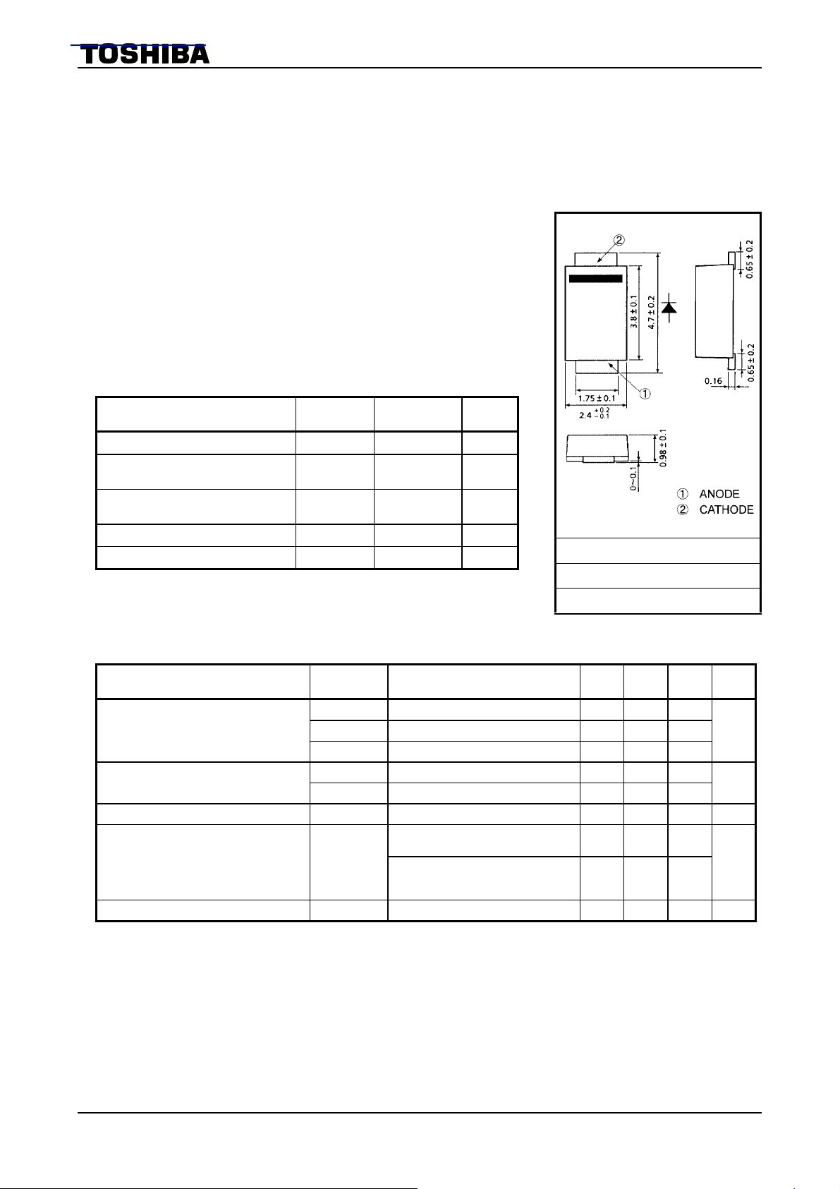
Unit: mm
JEDEC ―
JEITA ―
TOSHIBA 3-4E1A
Weight: 0.023 g (typ.)
Characteristics Symbol Test Condition Min Typ. Max Unit
V
IFM = 0.1 A ¾ 0.32 ¾
FM (1)
Peak forward voltage
Repetitive peak reverse current
Junction capacitance Cj VR = 10 V, f = 1.0 MHz ¾ 70 ¾ pF
Thermal resistance R
Thermal resistance R
V
IFM = 0.5 A ¾ 0.37 ¾
FM (2)
V
IFM = 1.0 A ¾ 0.40 0.45
FM (3)
I
V
RRM
I
V
RRM
th (j-a)
th (j-ℓ)
= 5 V ¾ 1.5 ¾
RRM
= 30 V ¾ 15.0 500
RRM
Device mounted on a ceramic board
(soldering land: 2 mm ´ 2 mm)
Device mounted on a glass-epoxy
board
(soldering land: 6 mm ´ 6 mm)
¾ ¾ ¾ 16 °C/W
¾ ¾ 60
¾ ¾ 135
°C/W
V
mA
1
2003-02-17
Page 2
CMS09
r
y
Marking Following Indicates the Data
of Manufacture
Type code
Lot No.
0 1 2 3 4
S9
Cathode mark
Month of
manufacture
Year of
manufacture
January to Decembe
are denoted by letter A
to L respectivel
Last decimal digit of
the year of
manufacture
.
5 6 7 8 9
Standard Soldering Pad
Unit: mm
2.1
1.4
3.0 1.4
Handling Precaution
Schottky barrier diodes are having large-reverse-current-leakage characteristic compare to the other rectifier
products. This current leakage and improper operating temperature or voltage may cause thermal runaway.
Please take forward and reverse loss into consideration when you design.
2
2003-02-17
Page 3

(
)
(
10
(A)
F
Tj = 150°C
125°C
i
F
– vF
75°C
1
25°C
Instantaneous forward current i
0.1
0.1 0.2 0.3 0.4 0.5 0.6 0.7 0.8
Instantaneous forward voltage vF (V)
Ta max (°C)
Maximum allowable ambient temperature
Device mounted on a glass-epoxy board
board size: 50 mm ´ 50 mm, land size 6 mm ´ 6 mm
160
140
120
100
80
60
40
20
0
0
0.2 0.4 0.6 0.8 1.0 1.2 1.4 1.6
Average forward current I
a = 60°
Ta m a x – I
a = 180°
a = 120°
F (AV)
DC
Conduction angle: a
F (AV)
500
(°C/W)
100
th (j-a)
Device mounted on a glass-epoxy board
Soldering land: 2.1 mm ´ 1.4 mm
10
1
Transient thermal impedance r
0.5
0.001 0.01 0.1 1 10 100 1000
Rectangular
waveform
360° 0° a
I
F (AV)
VR = 15 V
(A)
0.9
Average forward power dissipation
Maximum allowable ambient temperature
– t
r
th (j-a)
Device mounted on a ceramic board
Time t (s)
P
0.6
0.5
0.4
(W)
0.3
F (AV)
P
0.2
0.1
0
Rectangular
waveform
Conduction angle: a
0
0.2 0.4 0.6 0.8 1.0 1.2 1.4 1.6
Average forward current I
F (AV)
360°0° a
a = 120°
a = 60°
Ta m a x – I
Device mounted on a ceramic board
160
140
120
100
80
Ta max (°C)
60
40
20
0
0
Device mounted on a glass-epoxy board
Soldering land: 6.0 mm ´ 6.0 mm
Soldering land: 2.0 mm ´ 2.0 mm
board size: 50 mm ´ 50 mm)
a = 60°
Rectangular
waveform
360°0° a
I
Conduction angle: a
F (AV)
VR = 15 V
0.2 0.4 0.6 0.8 1.0 1.2 1.4 1.6
Average forward current I
– I
F (AV)
a = 180°
F (AV)
F (AV)
a = 180°
a = 120°
F (AV)
CMS09
DC
(A)
DC
(A)
3
2003-02-17
Page 4

CMS09
(A)
FSM
Surge forward current (non-repetitive)
28
24
20
16
12
8
4
Peak surge forward current I
0
1
I
100
Pulse test
10
(mA)
R
1
0.1
Reverse current I
0.01
0.001
0
40 140
20 8060 120 100
Junction temperature Tj (°C)
10 100
Number of cycles
– T
R
j
VR = 5 V
VR = 3 V
Ta = 25°C
f = 50 Hz
VR = 30 V
VR = 20 V
VR = 15 V
VR = 10 V
(typ.)
160
C
1000
(pF)
j
100
Junction capacitance C
10
1
Reverse voltage VR (V)
– VR (typ.)
j
f = 1 MHz
Ta = 25°C
10 100
P
Average reverse power dissipation
0.8
Rectangular waveform
0.7
0.6
0.5
(W)
0.4
R (AV)
0.3
P
0.2
0.1
0
0
360°
0°
V
R
a
Conduction angle: a
Tj = 150°C
10 30
Reverse voltage VR (V)
– VR (typ.)
R (AV)
240°
180°
120°
60°
DC
300°
20
4
2003-02-17
Page 5

CMS09
A
RESTRICTIONS ON PRODUCT USE
· TOSHIBA is continually working to improve the quality and reliability of its products. Nevertheless, semiconductor
devices in general can malfunction or fail due to their inherent electrical sensitivity and vulnerability to physical
stress. It is the responsibility of the buyer, when utilizing TOSHIBA products, to comply with the standards of
safety in making a safe design for the entire system, and to avoid situations in which a malfunction or failure of
such TOSHIBA products could cause loss of human life, bodily injury or damage to property.
In developing your designs, please ensure that TOSHIBA products are used within specified operating ranges as
set forth in the most recent TOSHIBA products specifications. Also, please keep in mind the precautions and
conditions set forth in the “Handling Guide for Semiconductor Devices,” or “TOSHIBA Semiconductor Reliability
Handbook” etc..
· The TOSHIBA products listed in this document are intended for usage in general electronics applications
(computer, personal equipment, office equipment, measuring equipment, industrial robotics, domestic appliances,
etc.). These TOSHIBA products are neither intended nor warranted for usage in equipment that requires
extraordinarily high quality and/or reliability or a malfunction or failure of which may cause loss of human life or
bodily injury (“Unintended Usage”). Unintended Usage include atomic energy control instruments, airplane or
spaceship instruments, transportation instruments, traffic signal instruments, combustion control instruments,
medical instruments, all types of safety devices, etc.. Unintended Usage of TOSHIBA products listed in this
document shall be made at the customer’s own risk.
· The information contained herein is presented only as a guide for the applications of our products. No
responsibility is assumed by TOSHIBA CORPORATION for any infringements of intellectual property or other
rights of the third parties which may result from its use. No license is granted by implication or otherwise under
any intellectual property or other rights of TOSHIBA CORPORATION or others.
· The information contained herein is subject to change without notice.
000707EA
5
2003-02-17
 Loading...