

Datasheet CM88L70CPEI, CM88L70CPE, CM88L70CP, CM88L70PEI, CM88L70PE Datasheet (California Micro Devices)
...Page 1
CALIFORNIA MICRO DEVICES
CM88L70/70C
CMOS INTEGRATED DTMF RECEIVER, 3 VOLT VERSION
Features
2.7 to 3.6 volt operating range
Full DTMF receiver
Less than 18mW power consumption
Industrial temperature range
Uses quartz crystal or ceramic resonators
Adjustable acquisition and release times
18-pin DIP, 20-pin QSOP, 18-pin SOIC,
20-pin PLCC, 20-pin TSSOP
CM88L70
- Power down mode
- Inhibit mode
- Buffered oscillator output (OSC 3) to
drive other devices
Product Description
The CAMD CM88L70/70C provides full DTMF receiver capability by integrating both the bandsplit filter and digital decoder
functions into a single 18-pin DIP, SOIC, or 20-pin PLCC, TSSOP, or QSOP package. The CM88L70/70C is manufactured using
state-of-the-art CMOS process technology for low power consumption (35mW, max.) and precise data handling. The filter
section uses a switched capacitor technique for both high and low group filters and dial tone rejection. The CM88L70/70C
decoder uses digital counting techniques for the detection and decoding of all 16 DTMF tone pairs into a 4-bit code. This
DTMF receiver minimizes external component count by providing an on-chip differential input amplifier, clock generator, and
a latched three-state interface bus. The on-chip clock generator requires only a low cost TV crystal or ceramic resonator as
an external component.
Applications
PCMCIA
Portable TAD
Mobile radio
Remote control
Remote data entry
Call limiting
Telephone answering systems
Paging systems
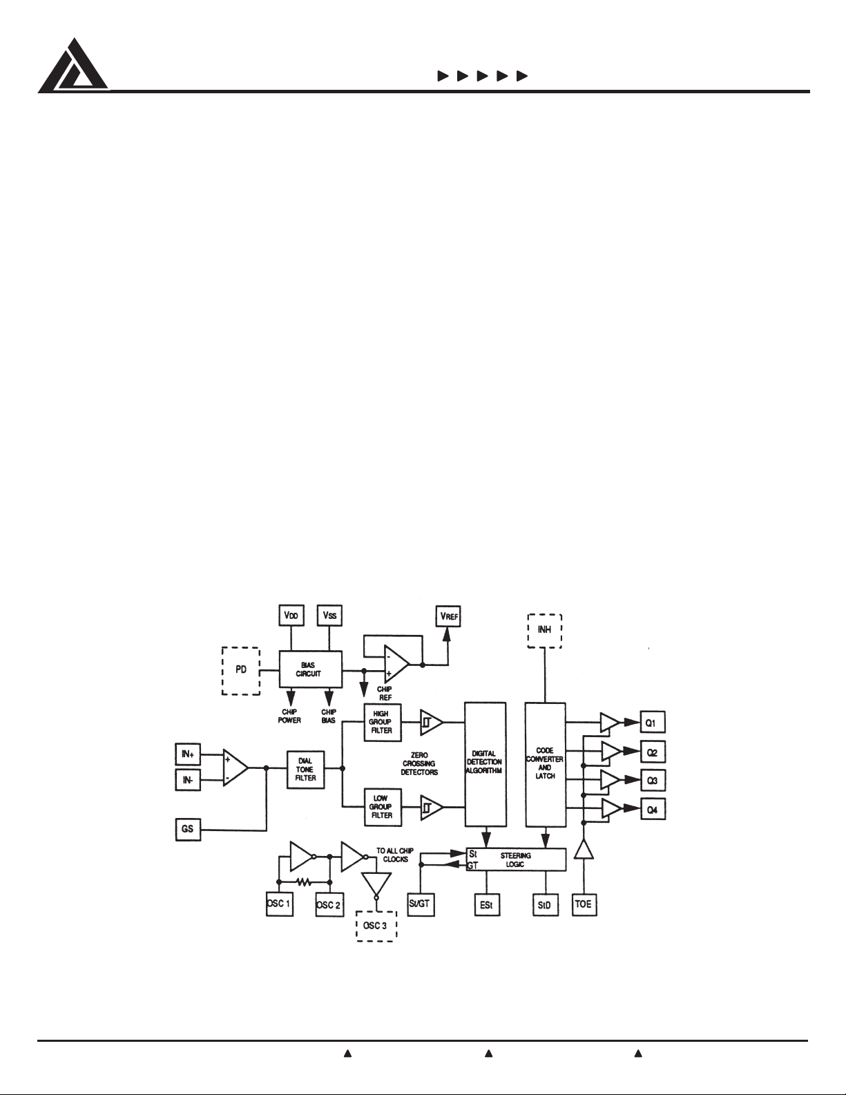
Block Diagram
© 2000 California Micro Devices Corp. All rights reserved.
6/16/2000
215 Topaz Street, Milpitas, California 95035 Tel: (408) 263-3214 Fax: (408) 263-7846 www.calmicro.com
C0451098
1
Page 2
CALIFORNIA MICRO DEVICES
CM88L70/70C
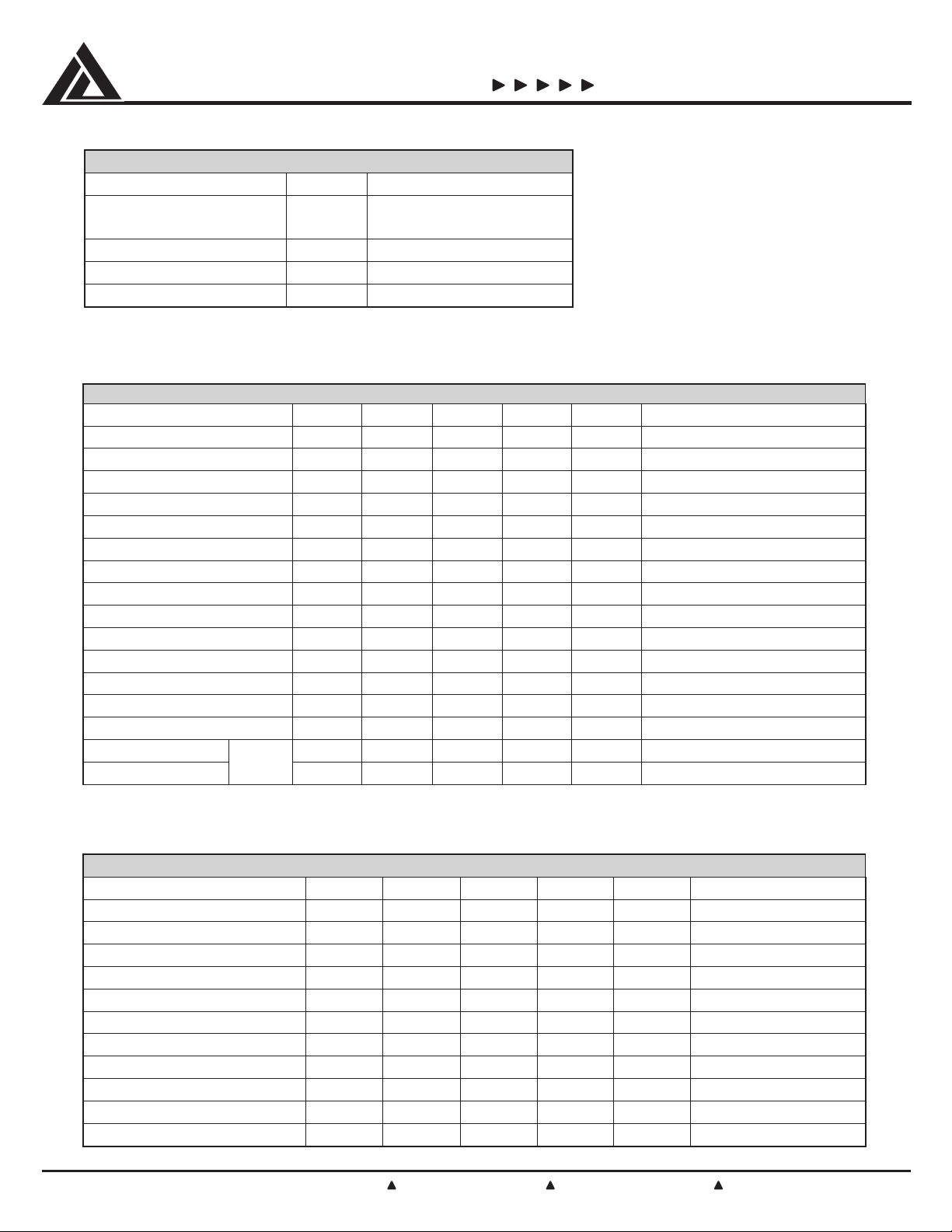
Absolute Maximum Ratings: (Note 1)
This device contains input protection against
damage due to high static voltages or
electric fields; however, precautions should
be taken to avoid application of voltages
higher than the maximum rating.
Note:
1. Exceeding these ratings may cause
permanent damage, functional
operation under these conditions is not
VSS)
retemaraPlobmySeulaV
-
V(egatloVylppuSrewoP
DD
niPynanoegatloVV
niPynanotnerruCI
erutarepmeTegarotST
V
DD
t
t
S
V
SS
SGNITARMUMIXAMETULOSBA
xaMV0.6
VotV3.0-
V3.0+
DD
xaMAm01
C°051+otC°56-
implied.
DC Characteristics: All voltages referenced to VSS, VDD = 3.0V + 20% / -10%, TA = -40°C to +85°C unless otherwise noted.
SCITSIRETCARAHCCD
retemaraPlobmySniMpyTxaMstinUsnoitidnoCtseT
egatloVylppuSgnitarepOV
tnerruCylppuSgnitarepOI
tnerruCylppuSybdnatSI
DD
DD
SDD
7.20.36.3V V
0.30.5Am
0.501
µA
V=DP
DD
egatloVtupnIleveLwoLVLI0.1V VDDV0.3=
egatloVtupnIleveLhgiHV
tnerruCegakaeLtupnII
EOTnotnerruC)ecruoS(pUlluPI
DPtnerruC)knis(nwodlluPI
HNItnerruC)knis(nwodlluPI
)-NI,+NI(,ecnadepmItupnIR
egatloVdlohserhTgnireetSV
egatloVtuptuOleveLwoLV
egatloVtuptuOleveLhgiHV
tnerruC)ecruoS(hgiHtuptuOI
egatloVtuptuO
ecnatsiseRtuptuOR
V
FER
HIL/LI
V
HI
os
DP
HNI
NI
tsT
LO
HO
HO
FER
RO
0.2VV
21-0.2-
1.0
0.154
0.154
µA
µA
µA
µA
VNIV=
SS
V0.3=
DD
Vro
DD
V0=EOT
V0.3=DP
V0.3=NHI
01MΩ zHK1@
5.1V
1.04.0V ILOAm0.1=
4.26.2VI
0.1AmV
TUO
004= µA
HO
V@V5.2=
DD
5.1V daoLoN
01
ΩΚ
)11etoN(
V7.2=
Operating Characteristics: All voltages referenced to VSS, VDD = 3.0V + 20% / -10%, TA = -40°C to +85°C unless otherwise noted.
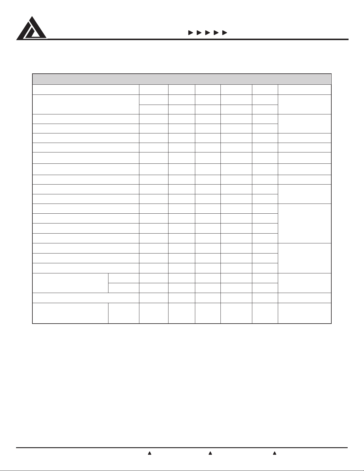
Gain Setting Amplifier
SCITSIRETCARAHCGNITAREPO
retemaraPlobmySniMpyTxaMstinUsnoitidnoCtseT
tnerruCegakaeLtupnII
ecnatsiseRtupnIR
egatloVtesffOtupnIV
noitcejeRylppuSrewoPRRSP0506Bd)21etoN(zHK1
noitcejeRedoMnommoCRRMC0406BdV<V0.3-
niaGegatloVpooLnepOCDA
gniwSegatloVtuptuOV
)SG(daoLeviticapaCelbareloTCL001Fp
)SG(daoLevitsiseRelbareloTR
©2000 California Micro Devices Corp. All rights reserved.
2
215 Topaz Street, Milpitas, California 95035 Tel: (408) 263-3214 Fax: (408) 263-7846 www.calmicro.com
NI
NI
SO
LOV
2356Bd
htdiwdnaBniaGytinUpooLnepOcf3.00.1zHM
O
L
)daoLoN(egnaRedoMnommoCmcV0.55.1V
001AnV
SS
01MΩ
5152Vm
2.2V
P-P
RL≥ K001 Ω Vot
KΩ
P-P
V<
V<
NI
DD
V0.3<
NI
SS
daoLoN
8/16/2000
Page 3
CALIFORNIA MICRO DEVICES
CM88L70/70C
AC Characteristics: All voltages referenced to V
using test circuit (Fig. 1) unless otherwise noted.
retemaraPlobmySniMpyTxaMstinUsetoN
sleveLlangiStupnIdilaV
)langisetisopmocfoenothcae(
tpeccAtsiwTevitisoP 6Bd
tpeccAtsiwTevitageN 6Bd
timiLtpeccAnoitaiveD.qerF zH2±%5.1.moN01,8,5,3,2
timiLtcejeRnoitaiveD.qerF%5.3±.moN5,3,2
ecnareloTenoTdrihT 61-Bd41,31,9,8,5,4,3,2
ecnareloTesioN21-Bd9,8,6,5,4,3,2
ecnareloTenoTlaiD 22+Bd9,8,7,5,4,3,2
emiTnoitceteDtneserPenoTt
emiTnoitceteDtnesbAenoTt
tpeccAnoitaruDenoTniMt
tcejeRnoitaruDenoTxaMt
tpeccAesuaPtigidretnI.niMt
tcejeResuaPtigidretnI.xaMt
)QottS(yaleDnoitagaporPt
)DtSottS(yaleDnoitagaporPt
)DtSotQ(pUteSataDtuptuOt
elbanEt
)QotEOT(yaleDnoitagaporP
elbasiDt
ycneuqerFkcolC/latsyrCf
)2CSO(tuptuOkcolCeviticapaC
daoL
PD
AD
CER
CER
DI
OD
QP
SPtD
SQtD
ETP
DTP
KLC
C
OL
, VDD=3.0V + 20% / -10%, TA=-40°C to +85°C, f
SS
SCITSIRETCARAHCCA
63-4.6-mBd
3.21073Vm
58 41Sm
5.03 5.8Sm
04Sm
02Sm
04Sm
02
31
8
4.3
002Sn
005Sn
9575.35975.31385.3zHM
03Fp
µS
µS
µS
µS
=3.579545 MHz
CLK
SMR
R
C
8,5,4,3,2,1
otrefeR
margaiDgnimiT
)elbatsujdAresU(
eranwohssemiT
htiwdeniatbo
)1.giFnitiucric
V=EOT
DD
K01= Ω
L
L
Fp05=
Notes:
1. dBm = decibels above or below a reference power
of 1 mW into a 600 ohm load.
2. Digit sequence consists of all 16 DTMF tones.
3. Tone duration = 40mS. Tone pause = 40 mS.
4. Nominal DTMF frequencies are used.
5. Both tones in the composite signal have
an equal amplitude.
6. Bandwidth limited (0 to 3 KHz) Gaussian Noise.
7. The precise dial tone frequencies are
(350 Hz and 440 Hz) ±2%.
8. For an error rate of better than 1 in 10,000
© 2000 California Micro Devices Corp. All rights reserved.
6/16/2000
215 Topaz Street, Milpitas, California 95035 Tel: (408) 263-3214 Fax: (408) 263-7846 www.calmicro.com
9. Referenced to lowest level frequency component
in DTMF signal.
10. Minimum signal acceptance level is measured with
specified maximum frequency deviation.
11. Input pins defined as IN+, IN-, and TOE.
12. External voltage source used to bias V
13. This parameter also applies to a third tone injected onto
.
REF
the power supply.
14. Referenced to Figure 1. Input DTMF tone level
at -28 dBm.
3
Page 4

CALIFORNIA MICRO DEVICES
CM88L70/70C
Explanation of Events
A) Tone bursts detected, tone duration invalid, outputs not
updated.
B) Tone #n detected, tone duration valid, tone decoded and
latched in outputs.
C) End of tone #n detected, tone absent duration valid,
outputs remain latched until next valid tone.
D) Outputs switched to high impedance state.
E) Tone #n + 1 detected, tone duration valid, tone decoded
and latched in outputs (currently high impedance).
F) Acceptable dropout of tone #n + 1, tone absent duration
invalid, outputs remain latched.
G) End of tone #n + 1 detected, tone absent duration valid,
outputs remain latched until next valid tone.
Explanation of Symbols
V
IN
DTMF composite input signal.
ESt Early Steering Output. Indicates detection
of valid tone frequencies.
St/GT Steering input/guard time output. Drives
external RC timing circuit.
Q1-Q4 4-bit decoded tone output.
StD Delayed Steering Output. Indicates that
valid frequencies have been present/absent
for the required guard time, thus constituting
a valid signal.
TOE Tone Output Enable (input). A low level
shifts Q1-Q4 to its high impedance state.
t
REC
Maximum DTMF signal duration not
detected as valid.
t
REC
Minimum DTMF signal duration required
for valid recognition.
t
ID
t
DO
Minimum time between valid DTMF signals.
Maximum allowable drop-out during valid
DTMF signal.
t
DP
Time to detect the presence of valid
DTMF signals.
t
DA
Time to detect the absence of valid
DTMF signals.
t
GTP
t
GTA
Guard time, tone present.
Guard time, tone absent.
©2000 California Micro Devices Corp. All rights reserved.
4
215 Topaz Street, Milpitas, California 95035 Tel: (408) 263-3214 Fax: (408) 263-7846 www.calmicro.com
8/16/2000
Page 5

CALIFORNIA MICRO DEVICES
CM88L70/70C
Functional Description
The CAMD CM88L70/70C DTMF Integrated Receiver provides the
design engineer with not only low power consumption, but high
performance in a small 18-pin DIP, SOIC, or 20-pin PLCC, TSSOP, or
QSOP package configuration. The CM88L70/70Cs internal
architecture consists of a bandsplit filter section which separates the
high and low tones of the received pair, followed by a digital decode
(counting) section which verifies both the frequency and duration of
the received tones before passing the resultant 4-bit code to the output
bus.
Filter Section
Separation of the low-group and high-group tones is achieved by
applying the dual-tone signal to the inputs of two 9
th
-order switched
capacitor bandpass filters. The bandwidths of these filters correspond
to the bands enclosing the low-group and high-group tones (See
Figure 3). The filter section also incorporates notches at 350 Hz and
440 Hz which provides excellent dial tone rejection. Each filter output
is followed by a single order switched capacitor section which smooths
the signals prior to limiting. Signal limiting is performed by high-gain
comparators. These comparators are provided with a hysteresis to
prevent detection of unwanted low-level signals and noise. The
outputs of the comparators provide full-rail logic swings at the
frequencies of the incoming tones.
Decoder Section
The CM88L70/70C decoder uses a digital counting technique to
determine the frequencies of the limited tones and to verify that these
tones correspond to standard DTMF frequencies. A complex averaging
algorithm is used to protect against tone simulation by extraneous
signals (such as voice) while providing tolerance to small frequency
variations. The averaging algorithm has been developed to ensure
an optimum combination of immunity to talk-off and tolerance to
the presence of interfering signals (third tones) and noise. When the
detector recognizes the simultaneous presence of two valid tones
(known as signal condition), it raises the Early Steering flag (ESt).
Any subsequent loss of signal condition will cause ESt to fall.
Steering Circuit
Before the registration of a decoded tone pair, the receiver checks for
a valid signal duration (referred to as character-recognitioncondition). This check is performed by an external RC time constant
driven by E
. A logic high on ESt causes VC (See Figure 4) to rise as
St
the capacitor discharges. Providing signal condition is maintained
(ESt remains high) for the validation period (t
threshold (V
) of the steering logic to register the tone pair, thus
TSt
), VC reaches the
GTP
latching its corresponding 4-bit code (See Figure 2) into the output
latch. At this point, the GT output is activated and drives VC to V
DD
GT continues to drive high as long as ESt remains high, signaling that
a received tone pair has been registered. The contents of the output
latch are made available on the 4-bit output bus by raising the threestate control input (TOE) to a logic high. The steering circuit works in
reverse to validate the interdigit pause between signals. Thus, as well
as rejecting signals too short to be considered valid, the receiver will
tolerate signal interruptions (drop outs) too short to be considered a
valid pause. This capability together with the capability of selecting
the steering time constants externally, allows the designer
to tailor
performance to meet a wide variety of system requirements.
Guard Time Adjustment
In situations which do not require independent selection of receive
and pause, the simple steering circuit of Figure 4 is applicable.
Component values are chosen according to the following formula:
= tDP + t
t
REC
t
» 0.67 RC
GTP
The value of t
GTP
is a parameter of the device and t
DP
is the minimum
REC
signal duration to be recognized by the receiver. A value for C of 0.1
uF is recommended for most applications, leaving R to be selected by
the designer. For example, a suitable value of R for a t
milliseconds would be 300K. A typical circuit using this steering
configuration is shown in Figure 1. The timing requirements for most
telecommunication applications are satisfied with this circuit. Different
steering arrangements may be used to select independently the
guardtimes for tone-present (t
) and tone absent (t
GTP
GTA
be necessary to meet system specifications which place both accept
and reject limits on both tone duration and interdigit pause.
Guard time adjustment also allows the designer to tailor system
parameters such as talk-off and noise immunity. Increasing t
improves talk-off performance, since it reduces the probability that
tones simulated by speech will maintain signal condition for long
enough to be registered. On the other hand, a relatively short t
with a long tDO would be appropriate for extremely noisy environments
where fast acquisition time and immunity to drop-outs would be
requirements. Design information for guard time adjustment is shown
in Figure 5.
Input Configuration
The input arrangement of the CM88L70/70C provides a differential
input operational amplifier as well as a bias source (V
used to bias the inputs at mid-rail.
Provision is made for connection of a feedback resistor to the opamp output (GS) for adjustment of gain.
In a single-ended configuration, the input pins are connected as shown
in Figure 1, with the op-amp connected for unity gain and VREF biasing
the input at ½ V
. Figure 6 shows the differential configuration,
DD
which permits the adjustment of gain with the feedback resistor R5.
Clock Circuit
The internal clock circuit is completed with the addition of a standard
television color burst crystal or ceramic resonator having a resonant
frequency of 3.579545 MHz. The CM8870C in a PLCC package has
a buffered oscillator output (OSC3) that can be used to drive clock
inputs of other devices such as a microprocessor or other CM887Xs
as shown in Figure 7. Multiple CM88L70/70Cs can be connected as
.
shown in figure 8 such that only one crystal or resonator is required.
Power Down and Inhibit Mode
A logic high applied to pin 6 (PD) will power down the device to
minimize the power consumption in a standby mode. It stops the
oscillator and functions of the filters.
Inhibit mode is enabled by a logic high input to the pin 5 (INH). It
inhibits the detection of tones representing characters A, B, C and
D. The output code will remain the same as the previous detected
code (see Figure 2).
of 40
REC
). This may
) which is
REF
REC
REC
© 2000 California Micro Devices Corp. All rights reserved.
6/16/2000
215 Topaz Street, Milpitas, California 95035 Tel: (408) 263-3214 Fax: (408) 263-7846 www.calmicro.com
5
Page 6

CALIFORNIA MICRO DEVICES
Pin Function Table
emaNnoitpircseD
+NI
-NI
SG
V
FER
HNI.D,C,B,AsyekstneserpersenotfonoitcetedstibihnI
3CSO.tuptuorotallicsodereffublatigiD
DPnwodrewoP
1CSOtupnikcolC
2CSOtuptuokcolC
V
SS
EOT QstuptuoehtselbanehgihcigoL.)tupni(elbanetuptuoetats-eerhT
Q
1
Q
2
Q
3
Q
4
DtS
tSE
tG/tS
V
DD
CIVotdeitebtsuM.noitcennoclanretnI
CM88L70/70C
tupnignitrevni-noN
tupnignitrevnI
.rotsiserkcabdeeffo
Vyllanimon(tuptuoegatlovecnerefeR
DD
.)V0otdetcennocyllamron(ylppusrewopevitageN
.)2.giFeeS(.deviecerriapenotdilav
.wolcigolaotnruterottSEesuaclliw
)2.giFeeS(.tSnoegatlovehtdnatSEfonoitcnufasietats
.ylppusrewopevitisoP
SS
1Q-4
)ylnonoitarugifnoc0788rof(
reifilpmalaitnereffiddne-tnorfehtotnoitcennoC
noitcennocrofreifilpmalaitnereffiddne-tnorffotuptuootsseccaseviG.tceleSniaG
.liar-dimtastupniehtsaibotdesuebyaM.)2/
.rotallicsoehtstibihnidnaecivedehtnwodsrewophgihcigoL
.rotallicsolanretnisetelpmocsnipesehtneewtebdetcennoclatsyrczHM545975.3
.pu-lluplanretnI.
tsalehtotgnidnopserrocedocehtsedivorp,EOTybdelbanenehW.stuptuoetats-eerhT
ehtdnaderetsigerneebsahriapenotdevieceranehwhgihcigolastneserP.tuptuognireetsdeyaleD
VwolebsllafTG/tSnoegatlovehtnehwwolcigolotsnruteR.detadpusihctaltuptuo
.
tST
mhtiroglalatigidehtnehwyletaidemmihgihcigolastneserP.tuptuognireetsylraE
noitidnoclangisfossolyratnemomynA.)noitidnoclangis(riapenotelbazingocerastceted
VnahtretaergegatlovA.)lanoitceridib(tuptuoemitdraug/tupnignireetS
tST
VnahtsselegatlovA.hctaltuptuoehtetadpudnariapenotdetcetedehtretsigerotecived
ehtsesuactStadetceted
tST
ehtseerf
stidna,tnatsnocemitgnireetslanretxeehtteserotstcatuptuoTGehT.riapenotwenatpeccaotecived
CM88L70
CM88L70C
All resistors are
All capacitors are
Figure 1. Single Ended Input Configuration Figure 2. Functional Diode Table
©2000 California Micro Devices Corp. All rights reserved.
6
215 Topaz Street, Milpitas, California 95035 Tel: (408) 263-3214 Fax: (408) 263-7846 www.calmicro.com
±±
±
1%tolerance.
±±
±±
±
5% tolerance.
±±
F
F
WOL
HGIH
YEKWOTQ4Q
Q
3
Q
2
1
7969021 1 H000 1
79663312H0010
79677413H0011
07790214H0100
07763315H0101
07777416H0110
25890217H0111
25863318H1000
25877419H1001
14990210H1010
1496331
●
H1011
1497741#H1100
7963361AH1101
0773361 B H 1110
2583361 C H 1111
1493361 D H 0000
-- YNA L ZZZZ
ecnadepmIhgiH=Z,hgiHcigoL=H,woLcigoL=L
8/16/2000
Page 7

CALIFORNIA MICRO DEVICES
CM88L70/70C
Figure 3. Typical Filter Characteristic
Figure 4. Basic Steering Circuit
Figure 5. Guard Time Adjustment
© 2000 California Micro Devices Corp. All rights reserved.
6/16/2000
215 Topaz Street, Milpitas, California 95035 Tel: (408) 263-3214 Fax: (408) 263-7846 www.calmicro.com
Figure 6. Differential Input Configuration
7
Page 8

CALIFORNIA MICRO DEVICES
CM88L70/70C
OSC1 OSC2 OSC3
30pF
Figure 7. CM88L70C Crystal Connection
(PLCC Package Only)
Pin Assignments
OSC1 of other CM887X’s
Clock input of other devices
CM88L70C
P Plastic DIP (18)
S SOIC (18)
Figure 8. CM88L70/70C Crystal Connection
TS TSSOP (20)
Q QSOP (20)
IN+
IN-
OSC1
3.58 Mhz 30pF 30pF
'
&
%
$
#
"
!
CM88L70/C
OSC1 OSC1OSC2 OSC2 OSC2
CM8870
Ordering Information
Example:
Product Identification Number
Package
P Plastic DIP (18) S SOIC (18)
PE PLCC (20) TS TSSOP (20)
Q QSOP (20)
Temperature/Processing
None 0
I -40
O
C to +70OC, ±5% P.S. Tol.
O
C to +85OC, ±5% P.S. Tol.
CM88L70C
PE PLCC (20)
CM88L70
CM88L70C P I
©2000 California Micro Devices Corp. All rights reserved.
8
215 Topaz Street, Milpitas, California 95035 Tel: (408) 263-3214 Fax: (408) 263-7846 www.calmicro.com
8/16/2000
 Loading...