

Page 1
CM17699
COLOR PDP DRIVER MODULE
PRODUCT PREVIEW
1 CM17699 MAIN FEATURES
2 CM17699 CONNECTORS DEFINITION
2.1 SIGNAL CONNECTOR. . . . . . . . . . . . . . . . . . . . . . . . . . . . . . . . . . . . . . . . . . . . . . . . . . 2
2.2 POWER SUPPLY CONNECTOR . . . . . . . . . . . . . . . . . . . . . . . . . . . . . . . . . . . . . . . . . . 2
3 CM17699 SCHEMATIC
3.1 DETAILS OF DIE BONDING. . . . . . . . . . . . . . . . . . . . . . . . . . . . . . . . . . . . . . . . . . . . . . 4
4 PCB MECHANICAL SPECIFICATIONS
5 FPC MECHANICAL SPECIFICATIONS
6 STV7699 SPECIFICATIONS
6.1 FEATURE S. . . . . . . . . . . . . . . . . . . . . . . . . . . . . . . . . . . . . . . . . . . . . . . . . . . . . . . . . . . 5
6.2 GENERAL DESCRIPTION . . . . . . . . . . . . . . . . . . . . . . . . . . . . . . . . . . . . . . . . . . . . . . . 5
6.3 PAD DIMENSIONS . . . . . . . . . . . . . . . . . . . . . . . . . . . . . . . . . . . . . . . . . . . . . . . . . . . . . 6
6.4 BLOCK DIAGRAM . . . . . . . . . . . . . . . . . . . . . . . . . . . . . . . . . . . . . . . . . . . . . . . . . . . . . 7
6.5 CIRCUIT DESCRIPTION . . . . . . . . . . . . . . . . . . . . . . . . . . . . . . . . . . . . . . . . . . . . . . . . 7
6.6 CHARACTERISTICS . . . . . . . . . . . . . . . . . . . . . . . . . . . . . . . . . . . . . . . . . . . . . . . . . . . 8
6.6.1 Absolute Maximum Ratings . . . . . . . . . . . . . . . . . . . . . . . . . . . . . . . . . . . . . . . . . . . . . . 8
6.6.2 Electrical Characteristics. . . . . . . . . . . . . . . . . . . . . . . . . . . . . . . . . . . . . . . . . . . . . . . . . 8
6.6.3 AC Timings Requirements . . . . . . . . . . . . . . . . . . . . . . . . . . . . . . . . . . . . . . . . . . . . . . . 9
6.6.4 AC Timings Characteristics . . . . . . . . . . . . . . . . . . . . . . . . . . . . . . . . . . . . . . . . . . . . . . . 9
6.7 INPUT/OUTPUT SCHEMATICS . . . . . . . . . . . . . . . . . . . . . . . . . . . . . . . . . . . . . . . . . . . 11
. . . . . . . . . . . . . . . . . . . . . . . . . . . . . . . . . . . . . . . . . . . . . 2
. . . . . . . . . . . . . . . . . . . . . . . . . . . . . . . . . . . . . 2
. . . . . . . . . . . . . . . . . . . . . . . . . . . . . . . . . . . . . . . . . . . . . . . . . 3
. . . . . . . . . . . . . . . . . . . . . . . . . . . . . . . . . . . . 5
. . . . . . . . . . . . . . . . . . . . . . . . . . . . . . . . . . . . . 5
. . . . . . . . . . . . . . . . . . . . . . . . . . . . . . . . . . . . . . . . . . . . . 5
January 1999
This is advance information on a new product now in development or undergoing evaluation. Details are subject to change without notice.
CM17699. TIF
1/11
Page 2
CM17699
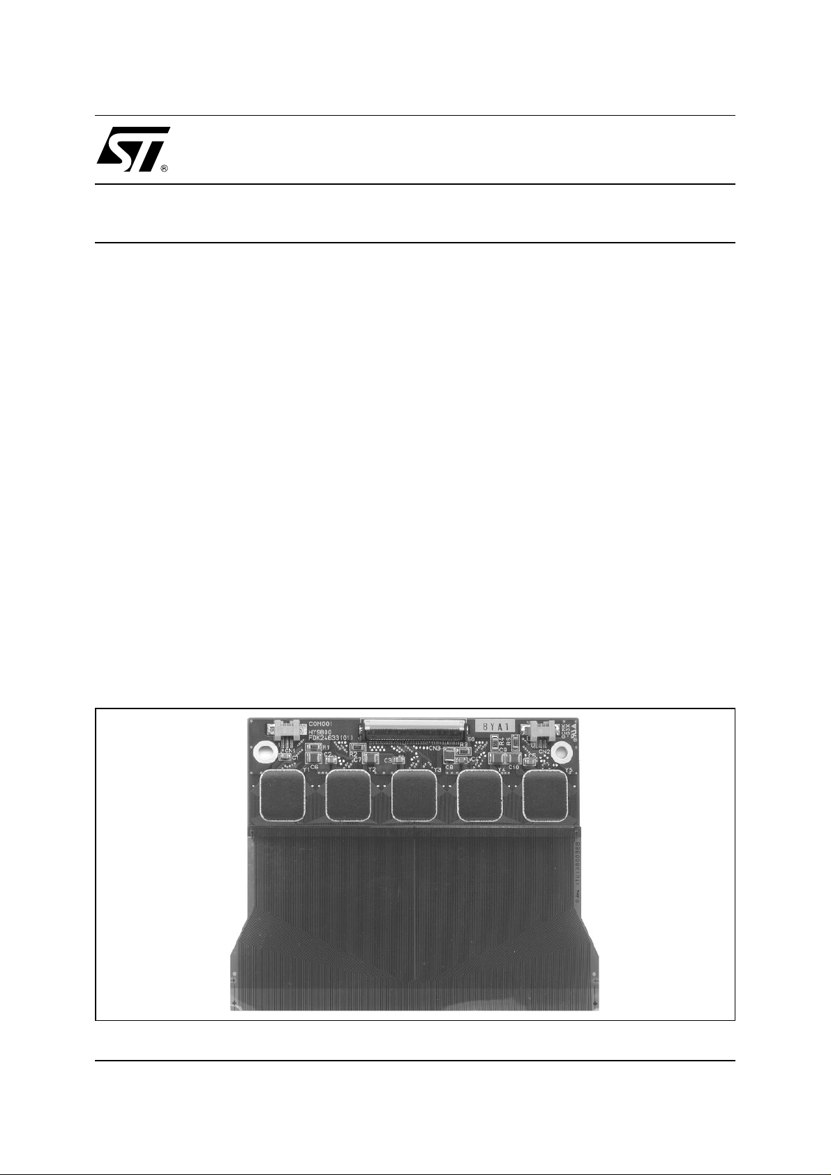
The CM17699 is plasma Display Panel (PDP) data
driver board implementing 5 data drivers referenced STV7699.
This module addresses 320 column electrodes of
a plasma panel. The monoblock structure of this
module and the output Flexible Printed Circuit
(FPC) realizes a high density package for data
drivers ICs. This module is adapted to standard
definition large size PDPs. The bidirectional feature
of this module allows its implementation on the top
side and/or bottom side of the panel without any
modification in the data bit stream.
1 - CM17699 MAIN FEATURE S
- Equiped with five STV7699 devices - 4 x 16-bit
bidirectional shift register
- Mounted connectors/capacitors
- Configurable for AC/DC power supply
- FPC compatible with narrow pitches of column
electrodes
- Compatible with custom designs.
Output Count 320
Output Pitch 320mm
Logic Power Supply 4.5V to 5.5V
Power Supply Voltage 30V to 160V
Power Output Current
Clock Frequency 20MHz
Dimension COB - 92 x 33
±
40mA
FPC - 101.4 x 50
2 - CM17699 CONNECTORS DEFINITION
2.1 - Signal Connector
Input signal connector is a 50 nodes high density
connector defined as follow :
1A14
2A13
3A12
4A11
5B11
6B12
7B13
8B14
9A24
10 A23
11 A22
12 A21
13 B21
14 B22
15 B2 3
16 B2 4
17 A3 4
18 A3 3
19 A3 2
20 A3 1
21 B3 1
22 B3 2
23 B3 3
24 B3 4
25 BLK
26 VS S
27 POL
28 VS S
29 F/R
30 VS S
31 STB
32 VS S
33 CLK
34 VS S
35 A44
36 A43
37 A42
38 A41
39 B41
40 B42
41 B43
42 B44
43 A54
44 A53
45 A52
46 A51
47 B51
48 B53
49 B53
50 B54
2.2 - Power Supply Connector
Power supplies come from 2 connectors of 3 nodes
each (V
, VDD, VSS). The use of both connectors
PP
is not necessary as all the supplies are connected
together on the board. The use of both connectors
spread the currents on the PC borad and reduce
the EMI radiations.
Depending on the application, the data module can
be configured either for DC supplies or for AC
supplies of the data drivers by the implementation
of surface mounted devices.
2/11
Page 3
CM17699
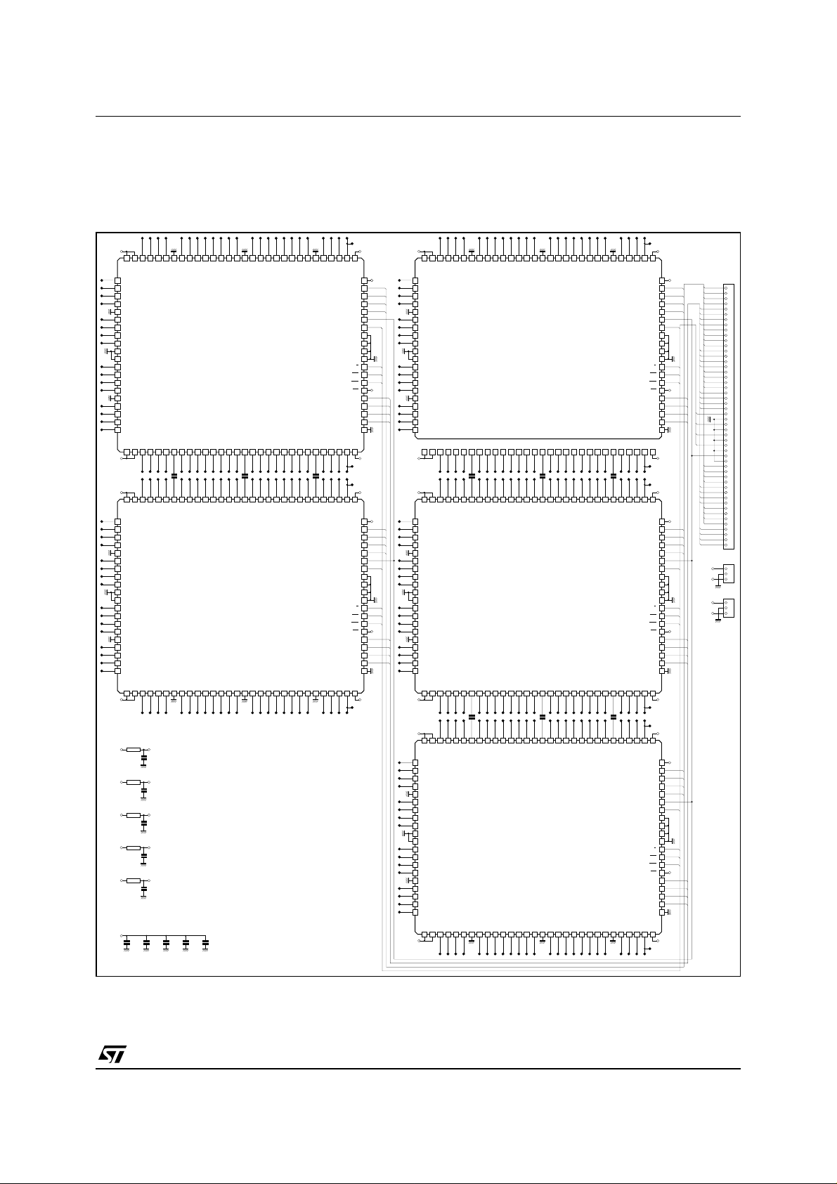
3 - CM17699 SCHEMA T IC
Decoupling capacitors must be located as close as possible to the drivers. If the damping and protection
resistor in V
Figure 1
V
PP4
IC4
30 29 28 27 26 25 24 23 22 21 20 19 18 17 16 15 14 13 12 11 10 9 8 7 6 5 4 3 2 1
PP
VPPV
04-25
31
OUT25
04-26
32
OUT26
04-27
33
OUT27
04-28
34
OUT28
35
V
SSP
04-29
36
OUT29
04-30
37
OUT30
04-31
38
OUT31
04-32
39
OUT32
40
V
SSP
41
V
SSSUB
04-33
42
OUT33
04-34
43
OUT34
04-35
44
OUT35
04-36
45
OUT36
46
V
SSP
04-37
47
OUT37
04-38
48
OUT38
04-39
49
OUT39
04-40
50
OUT40
PP
VPPV
51 52 53 54 55 56 57 58 59 60 61 62 63 64 65 66 67 68 69 70 71 72 73 74 75 76 77 78 79 80
V
PP4
V
PP5
IC5
30 29 28 27 26 25 24 23 22 21 20 19 18 17 16 15 14 13 12 11 10 9 8 7 6 5 4 3 2 1
PP
VPPV
05-25
31
OUT25
05-26
32
OUT26
05-27
33
OUT27
05-28
34
OUT28
35
V
SSP
05-29
36
OUT29
05-30
37
OUT30
05-31
38
OUT31
05-32
39
OUT32
40
V
SSP
41
V
SSSUB
05-33
42
OUT33
05-34
43
OUT34
05-35
44
OUT35
05-36
45
OUT36
46
V
SSP
05-37
47
OUT37
05-38
48
OUT38
05-39
49
OUT39
05-40
50
OUT40
PP
VPPV
51 52 53 54 55 56 57 58 59 60 61 62 63 64 65 66 67 68 69 70 71 72 73 74 75 76 77 78 79 80
V
PP4
R1
0 or 22
W
V
PP
C1-1
68nF
R2
0 or 22
W
V
PP
C1-2
68nF
R3
0 or 22
W
V
PP
C1-3
68nF
R4
0 or 22
W
V
PP
C1-4
68nF
R5
0 or 22
W
V
PP
C1-5
68nF
V
CC
C1
100nFC2100nFC3100nFC4100nFC5100nF
line of each driver is different to 0Ω, the decoupling capacitor should not be mounted.
PP
04-24
04-23
04-22
OUT22
OUT23
OUT24
OUT41
OUT42
OUT43
04-41
04-42
04-43
05-24
05-23
05-22
OUT22
OUT23
OUT24
OUT41
OUT42
OUT43
05-41
05-42
05-43
V
PP1
(not connect if R = 22
V
PP2
(not connect if R = 22
V
PP3
(not connect if R = 22
V
PP4
(not connect if R = 22
V
PP5
(not connect if R = 22
TP4-1
V
04-21
04-19
04-20
04-18
04-17
04-16
04-15
04-14
04-13
04-11
04-12
04-10
04-9
04-8
04-7
04-6
04-5
04-4
SSP
V
OUT18
OUT19
OUT20
OUT21
SSP
V
OUT10
OUT12
OUT13
OUT14
OUT15
OUT16
OUT17
OUT11
SSP
V
OUT5
OUT6
OUT7
OUT8
OUT9
STV7699
(Die)
SSP
OUT44
OUT45
OUT46
OUT47
V
04-44
04-45
04-46
04-47
05-21
05-19
05-20
05-18
SSP
V
OUT18
OUT19
OUT20
OUT21
SSP
OUT48
OUT49
OUT50
OUT51
OUT52
OUT53
OUT54
OUT55
V
04-48
04-50
04-51
04-52
04-53
04-54
04-49
05-17
05-16
05-15
OUT15
OUT16
OUT17
04-55
05-14
05-13
05-11
05-12
05-10
SSP
V
OUT10
OUT12
OUT13
OUT14
OUT11
SSP
OUT56
OUT57
OUT58
OUT59
OUT60
V
04-56
04-57
04-58
04-59
04-60
04-61
05-9
05-8
05-7
05-6
05-5
05-4
SSP
V
OUT5
OUT6
OUT7
OUT8
OUT9
STV7699
(Die)
SSP
OUT44
OUT45
OUT46
OUT47
V
05-44
05-45
05-46
05-47
W
)
)
W
W
)
)
W
W
)
SSP
OUT48
OUT49
OUT50
OUT51
OUT52
OUT53
OUT54
OUT55
V
05-48
05-50
05-51
05-52
05-53
05-54
05-49
05-55
SSP
OUT56
OUT57
OUT58
OUT59
OUT60
V
05-56
05-57
05-58
05-59
05-60
05-61
PP4
04-3
04-2
04-1
PP
V
OUT1
OUT2
OUT3
OUT4
100
V
CC
99
A1
98
A2
97
A3
96
A4
95
CLK
94
STB
93
V
SSLOG
92
V
SSLOG
91
V
SSLOG
90
V
SSLOG
89
F/R
88
BLK
87
POL
86
HIZ
85
B4
84
B3
83
B2
82
B1
81
V
SSSUB
PP
OUT61
OUT62
OUT63
OUT64
V
V
PP4
04-62
04-63
04-64
TP4-2
TP5-1
V
PP5
05-3
05-2
05-1
PP
V
OUT1
OUT2
OUT3
OUT4
100
V
CC
99
A1
98
A2
97
A3
96
A4
95
CLK
94
STB
93
V
SSLOG
92
V
SSLOG
91
V
SSLOG
90
V
SSLOG
89
F/R
88
BLK
87
POL
86
HIZ
85
B4
84
B3
83
B2
82
B1
81
V
SSSUB
PP
OUT61
OUT62
OUT63
OUT64
V
V
PP5
05-62
05-63
05-64
TP5-2
V
PP1
01-24
01-23
01-22
01-21
01-19
01-20
01-18
01-17
01-16
01-15
01-14
01-13
01-11
01-12
01-10
01-9
01-8
01-7
01-6
IC1
30 29 28 27 26 25 24 23 22 21 20 19 18 17 16 15 14 13 12 11 10 9 8 7 6 5 4 3 2 1
PP
01-25
31
V
CC
A41
A42
A43
A44
ST
F/R
BL
PO
V
CC
B44
B43
B42
B41
V
CC
A51
A52
A53
A54
ST
F/R
BL
PO
V
CC
B54
B53
B52
B51
OUT25
01-26
32
OUT26
01-27
33
OUT27
01-28
34
OUT28
35
V
SSP
01-29
36
OUT29
01-30
37
OUT30
01-31
38
OUT31
01-32
39
OUT32
40
V
SSP
41
V
SSSUB
01-33
42
OUT33
01-34
43
OUT34
01-35
44
OUT35
01-36
45
OUT36
46
V
SSP
01-37
47
OUT37
01-38
48
OUT38
01-39
49
OUT39
01-40
50
OUT40
VPPV
51 52 53 54 55 56 57 58 59 60 61 62 63 64 65 66 67 68 69 70 71 72 73 74 75 76 77 78 79 80
V
PP1
V
PP2
IC2
30 29 28 27 26 25 24 23 22 21 20 19 18 17 16 15 14 13 12 11 10 9 8 7 6 5 4 3 2 1
PP
02-25
31
OUT25
02-26
32
OUT26
02-27
33
OUT27
02-28
34
OUT28
35
V
SSP
02-29
36
OUT29
02-30
37
OUT30
02-31
38
OUT31
02-32
39
OUT32
40
V
SSP
41
V
SSSUB
02-33
42
OUT33
02-34
43
OUT34
02-35
44
OUT35
02-36
45
OUT36
46
V
SSP
02-37
47
OUT37
02-38
48
OUT38
02-39
49
OUT39
02-40
50
OUT40
VPPV
51 52 53 54 55 56 57 58 59 60 61 62 63 64 65 66 67 68 69 70 71 72 73 74 75 76 77 78 79 80
V
PP2
V
PP3
IC3
30 29 28 27 26 25 24 23 22 21 20 19 18 17 16 15 14 13 12 11 10 9 8 7 6 5 4 3 2 1
PP
03-25
31
OUT25
03-26
32
OUT26
03-27
33
OUT27
03-28
34
OUT28
35
V
SSP
03-29
36
OUT29
03-30
37
OUT30
03-31
38
OUT31
03-32
39
OUT32
40
V
SSP
41
V
SSSUB
03-33
42
OUT33
03-34
43
OUT34
03-35
44
OUT35
03-36
45
OUT36
46
V
SSP
03-37
47
OUT37
03-38
48
OUT38
03-39
49
OUT39
03-40
50
OUT40
VPPV
51 52 53 54 55 56 57 58 59 60 61 62 63 64 65 66 67 68 69 70 71 72 73 74 75 76 77 78 79 80
V
PP3
SSP
VPPV
V
OUT18
OUT19
OUT20
OUT22
OUT23
OUT24
OUT21
PP
SSP
OUT41
OUT42
OUT43
OUT44
OUT45
OUT46
OUT47
V
01-41
01-42
01-43
01-44
01-45
01-46
01-47
02-24
02-23
02-22
02-21
02-19
02-20
02-18
SSP
VPPV
V
OUT18
OUT19
OUT20
OUT22
OUT23
OUT24
OUT21
PP
SSP
OUT41
OUT42
OUT43
OUT44
OUT45
OUT46
OUT47
V
02-41
02-42
02-43
02-44
02-45
02-46
02-47
03-24
03-23
03-22
03-21
03-19
03-20
03-18
SSP
VPPV
V
OUT18
OUT19
OUT20
OUT22
OUT23
OUT24
OUT21
PP
SSP
OUT41
OUT42
OUT43
OUT44
OUT45
OUT46
OUT47
V
03-41
03-42
03-43
03-44
03-45
03-46
03-47
OUT15
OUT16
OUT17
STV7699
OUT48
OUT49
OUT50
01-48
01-50
01-49
02-17
02-16
02-15
OUT15
OUT16
OUT17
STV7699
OUT48
OUT49
OUT50
02-48
02-50
02-49
03-17
03-16
03-15
OUT15
OUT16
OUT17
STV7699
OUT48
OUT49
OUT50
03-48
03-50
03-49
OUT13
OUT14
(Die)
OUT51
OUT52
01-51
01-52
02-14
02-13
OUT13
OUT14
(Die)
OUT51
OUT52
02-51
02-52
03-14
03-13
OUT13
OUT14
(Die)
OUT51
OUT52
03-51
03-52
SSP
V
OUT12
OUT11
SSP
OUT53
OUT54
V
01-53
01-54
02-11
02-12
SSP
V
OUT12
OUT11
SSP
OUT53
OUT54
V
02-53
02-54
03-11
03-12
SSP
V
OUT12
OUT11
SSP
OUT53
OUT54
V
03-53
03-54
01-5
SSP
V
OUT5
OUT6
OUT7
OUT8
OUT9
OUT10
OUT55
01-55
02-10
OUT10
OUT55
02-55
03-10
OUT10
OUT55
03-55
SSP
OUT56
OUT57
OUT58
OUT59
OUT60
V
01-56
01-57
01-58
01-59
01-60
02-9
02-8
02-7
02-6
02-5
SSP
V
OUT5
OUT6
OUT7
OUT8
OUT9
SSP
OUT56
OUT57
OUT58
OUT59
OUT60
V
02-56
02-57
02-58
02-59
02-60
03-9
03-8
03-7
03-6
03-5
SSP
V
OUT5
OUT6
OUT7
OUT8
OUT9
SSP
OUT56
OUT57
OUT58
OUT59
OUT60
V
03-56
03-57
03-58
03-59
03-60
TP1-1
V
01-4
01-61
02-4
02-61
03-4
03-61
PP1
01-3
01-2
01-1
PP
V
OUT1
OUT2
OUT3
OUT4
100
V
V
CC
CC
A11
99
A1
A12
98
A2
A13
97
A3
A14
96
A4
95
CLK
ST
94
STB
93
V
SSLOG
92
V
SSLOG
91
V
SSLOG
90
V
SSLOG
F/R
89
F/R
BL
88
BLK
PO
87
POL
86
V
HIZ
CC
B14
85
B4
B13
84
B3
B12
83
B2
B11
82
B1
81
V
SSSUB
PP
OUT61
OUT62
OUT63
OUT64
V
V
PP1
01-62
01-63
01-64
TP1-2
TP2-1
V
PP2
02-3
02-2
02-1
PP
V
OUT1
OUT2
OUT3
OUT4
100
V
V
CC
CC
A21
99
A1
A22
98
A2
A23
97
A3
A24
96
A4
95
CLK
ST
94
STB
93
V
SSLOG
92
V
SSLOG
91
V
SSLOG
90
V
SSLOG
F/R
89
F/R
BL
88
BLK
PO
87
POL
86
V
HIZ
CC
B24
85
B4
B23
84
B3
B22
83
B2
B21
82
B1
81
V
SSSUB
PP
OUT61
OUT62
OUT63
OUT64
V
V
PP2
02-62
02-63
02-64
TP2-2
TP3-1
V
PP3
03-3
03-2
03-1
PP
V
OUT1
OUT2
OUT3
OUT4
100
V
V
CC
CC
A31
99
A1
A32
98
A2
A33
97
A3
A34
96
A4
95
CLK
ST
94
STB
93
V
SSLOG
92
V
SSLOG
91
V
SSLOG
90
V
SSLOG
F/R
89
F/R
BL
88
BLK
PO
87
POL
86
V
HIZ
CC
B34
85
B4
B33
84
B3
B32
83
B2
B31
82
B1
81
V
SSSUB
PP
OUT61
OUT62
OUT63
OUT64
V
V
PP3
03-62
03-63
03-64
TP3-2
J1
A14
1
A13
2
A12
3
A11
4
B11
5
B12
6
B13
7
B14
8
A24
9
A23
10
A22
11
A21
12
B21
13
B22
14
B23
15
B24
16
A34
17
A33
18
A32
19
A31
20
B31
21
B32
22
B33
23
B34
24
BL
25
26
PO
27
28
F/R
29
30
ST
31
32
33
34
A44
35
A43
36
A42
37
A41
38
B41
39
B42
40
B43
41
B44
42
A54
43
A53
44
A52
45
A51
46
B51
47
B52
48
B53
49
B54
50
CON50
J2
1
V
CC
2
3
V
PP
CON3
J3
1
V
CC
2
3
V
PP
CON3
3/11
7699C-01.EPS
Page 4
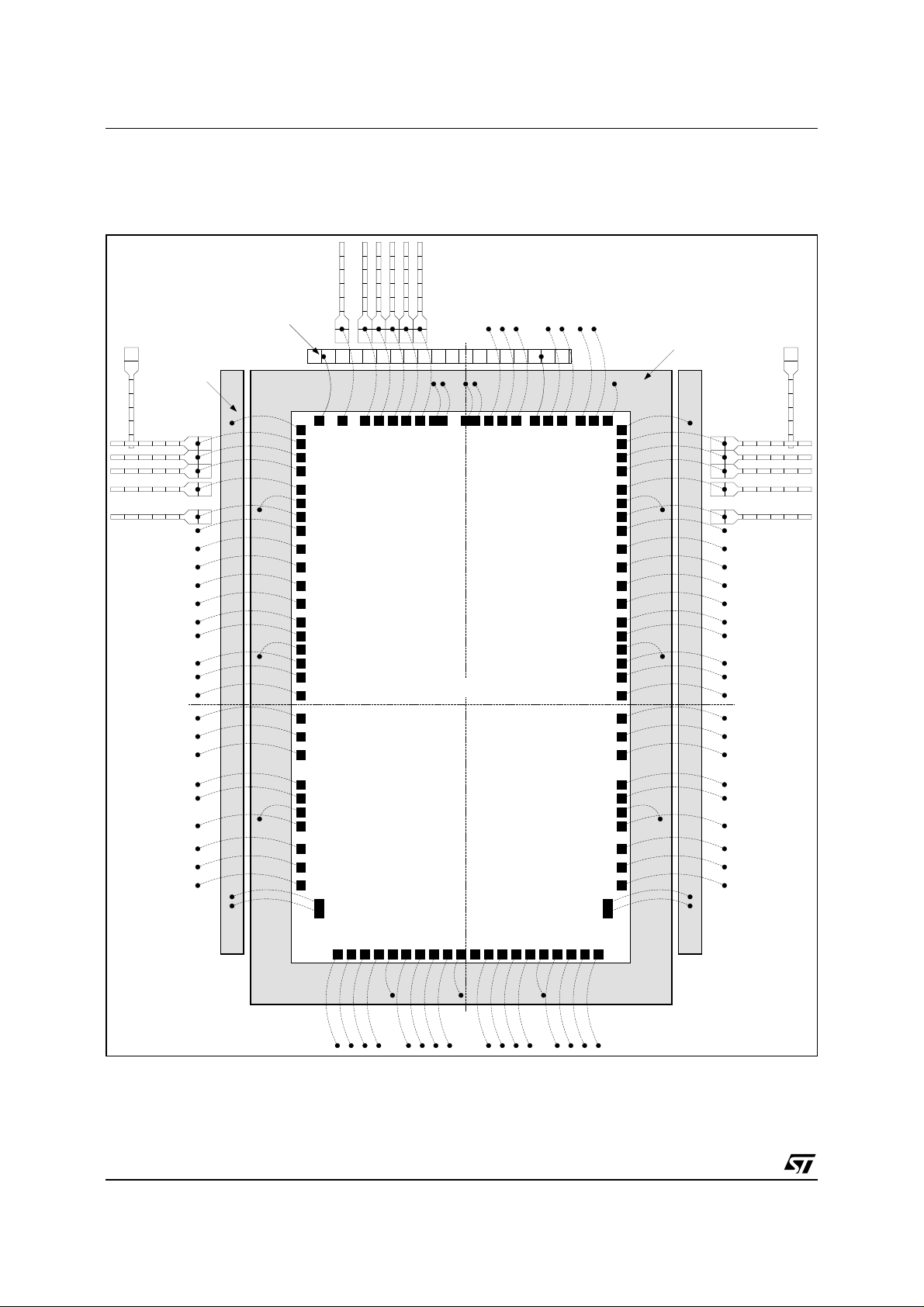
CM17699
3 - CM17699 SCHEMA T IC
(continued)
3.1 - Details of Die Bonding
Figure 2
V
OUT1
OUT2
OUT3
OUT4
OUT5
OUT6
OUT7
OUT8
OUT9
OUT10
OUT11
OUT12
OUT13
OUT14
OUT15
OUT16
OUT17
OUT18
CC
V
SS
V
V
SSLOG
SSLOG
STB
V
A1
CC
V
PP
V
SS
V
SS
CLK
A4
A3
A2
POL
BLK
HIZ
F/R
B3
B4
STV7699
V
SSSUB
B1
B2
V
PP
OUT64
OUT63
OUT62
OUT61
V
SS
OUT60
OUT59
OUT58
OUT57
OUT56
OUT55
OUT54
OUT53
V
SS
OUT52
OUT51
OUT50
OUT49
OUT48
OUT47
Test Point Test Point
V
PP
4/11
OUT19
OUT20
OUT21
OUT22
OUT23
OUT24
OUT46
OUT45
V
SS
V
PP
OUT25
OUT26
OUT27
OUT28
VSSOUT29
OUT30
OUT31
OUT32
V
V
OUT33
SS
SSSUB
V
OUT34
OUT35
OUT36
OUT37
OUT38
OUT39
SS
V
SS
OUT44
OUT43
OUT42
OUT41
V
PP
OUT40
7699C-02.EPS
Page 5

4 - PCB MECHANICAL SPECIFICATIONS
The rigid board is 92mm long by 30mm wide.
The rigid board can be mounted on the mechanical
chassis of the plasma panel or on a heat sinker by
clips and/or screws.
The recommended size of the heat sinker depends
Figure 3
92.0mm
3.3mm
CM17699
on the final application if data drivers are powered
with a DC or an AC supply .
Power supplies (V
copper surface in order to spread the current on the
board and reduce voltage drops and EMI.
, VSS) are dispatched by large
PP
CN1 & CN2 : JAE IL-3PL-SMTY-E1500
CN3 : JAE IL-FHR-50S-HF-E3000
9.60mm
31 50 1 3
9.60mm
CN2 CN3 CN1
35.1mm5mm
10.9mm 10.9mm
5 - FPC MECHANICAL SPECIFICATIONS
Figure 4
101.4mm
P 0.3 x (324-1) x 0.9991 = 96.81279 W = 0.15
10.0mm
Ø 0.5mm
1.25mm
1.2mm
P 0.25961 x (326-1) = 84.37325 W = 0.1
FPC specifications (UPILEX otherwise thermal expansion specified)
Cu Foil : 35
Ni Plating : > 1
Au Plating : > 0.1
m
m
m
m
m
m
4mm
4.7mm
3mm 5mm
PCB
Design values :
Conductor width = 0.15 ± 0.04
Gap width = 0.15 ± 0.04
Bonding
33.0mm
5mm
LCD
Bonding
6mm
15.0mm
50.0mm
7699C-03.EPS
2.25
1.15
1.4
1.4
3.75
0.15
2.0
0.40.40.4
0.4 0.4 0.4
3
7699C-04.EPS
6 - STV7699 SPECIFICA T ION S
6.1 - Features
- 64 outputs plasma display driver
- 170V absolute maximum supply
- 5V supply for logic
- 50/40mA source / sink output
- 60/60mA source / sink output diode
- 64-bit shift register (20MHz)
- BLK, polarity and HIZ control
- BCD technology
6.2 - General Description
The STV7699 is a Plasma Display Panel (PDP) data
driver implemented in ST’s proprietary BCD technology. Using a 4-bit wide cascadable shift register,
it drives 64 high current & high voltage outputs.
By serialy connecting several STV7699, an y horizontal pixel definition can be performed. The 20MHz
shift clock gives an eq uivalent 80MHz shift register.
The STV7699 is supplied with a separated 170V
power output s upply an d a 5V logic supply. A l l command inputs are CMOS compatible.
5/11
Page 6

CM17699
6 - STV7699 SPECIFICA T ION S
6.3 - Pad Dimensions
(in µm)
(continued)
The reference is the center of the die (x = 0, y = 0).
LEFT SIDE from top to bottom
Name Center : X Center : Y Size : x Size : y
V
PP
OUT1 -1738.0 2703.0 90.0 75.0
OUT2 -1738.0 2570.5 90.0 75.0
OUT3 -1738.0 2411.0 90.0 75.0
OUT4 -1738.0 2228.5 90.0 75.0
V
SSP
OUT5 -1738.0 1952.0 90.0 75.0
OUT6 -1738.0 1813.5 90.0 75.0
OUT7 -1738.0 1631.0 90.0 75.0
OUT8 -1738.0 1453.0 90.0 75.0
OUT9 -1738.0 1235.5 90.0 75.0
OUT10 -1738.0 1046.5 90.0 75.0
OUT11 -1738.0 862.0 90.0 75.0
OUT12 -1738.0 712.5 90.0 75.0
V
SSP
OUT13 -1738.0 431.0 90.0 75.0
OUT14 -1738.0 293.0 90.0 75.0
OUT15 -1738.0 82.5 90.0 75.0
OUT16 -1738.0 -109.5 90.0 75.0
OUT17 -1738.0 -277.0 90.0 75.0
OUT18 -1738.0 -471.0 90.0 75.0
OUT19 -1738.0 -691.5 90.0 75.0
OUT20 -1738.0 -822.5 90.0 75.0
V
SSP
OUT21 -1738.0 -1096.0 90.0 75.0
OUT22 -1738.0 -1335.5 90.0 75.0
OUT23 -1738.0 -1569.0 90.0 75.0
OUT24 -1738.0 -1697.5 90.0 75.0
V
PP
-1738.0 2867.5 90.0 75.0
-1738.0 2093.0 90.0 75.0
-1738.0 566.0 90.0 75.0
-1738.0 -953.0 90.0 75.0
-1715.0 -2045.0 90.0 200.0
Right SIDE from bottom to top
Name Center : X Center : Y Size : x Size : y
V
PP
OUT41 1737.5 -1646.0 90.0 75.0
OUT42 1737.5 -1507.0 90.0 75.0
OUT43 1737.5 -1328.0 90.0 75.0
OUT44 1737.5 -1096.0 90.0 75.0
V
SSP
OUT45 1737.5 -822.5 90.0 75.0
OUT46 1737.5 -691.5 90.0 75.0
OUT47 1737.5 -471.0 90.0 75.0
OUT48 1737.5 -277.0 90.0 75.0
OUT49 1737.5 -109.5 90.0 75.0
OUT50 1737.5 82.5 90.0 75.0
OUT51 1737.5 293.0 90.0 75.0
OUT52 1737.5 431.0 90.0 75.0
VSSP 1737.5 566.0 90.0 75.0
OUT53 1737.5 712.5 90.0 75.0
OUT54 1737.5 862.0 90.0 75.0
OUT55 1737.5 1046.5 90.0 75.0
OUT56 1737.5 1235.5 90.0 75.0
OUT57 1737.5 1453.0 90.0 75.0
OUT58 1737.5 1631.0 90.0 75.0
OUT59 1737.5 1813.5 90.0 75.0
OUT60 1737.5 1952.0 90.0 75.0
V
SSP
OUT61 1737.5 2228.5 90.0 75.0
OUT62 1737.5 2411.0 90.0 75.0
OUT63 1737.5 2570.5 90.0 75.0
OUT64 1737.5 2703.0 90.0 75.0
V
PP
1600.5 -2087.0 90.0 200.0
1737.5 -953.0 90.0 75.0
1737.5 2093.0 90.0 75.0
1737.5 2873.5 90.0 75.0
BOTTOM SIDE from left to right
Name Center : X Center : Y Size : x Size : y
OUT25 -1443.5 -3077.0 75.0 90.0
OUT26 -1249.0 -3077.0 75.0 90.0
OUT27 -1049.5 -3077.0 75.0 90.0
OUT28 -889.0 -3077.0 5.0 90.0
V
SSP
OUT29 -614.0 -3077.0 75.0 90.0
OUT30 -467.5 -3077.0 75.0 90.0
OUT31 -332.0 -3077.0 75.0 90.0
OUT32 -186.5 -3077.0 75.0 90.0
V
SSP
V
SSSUB
OUT33 209.5 -3077.0 75.0 90.0
OUT34 342.5 -3077.0 75.0 90.0
OUT35 467.5 -3077.0 75.0 90.0
OUT36 607.5 -3077.0 75.0 90.0
V
SSP
OUT37 892.5 -3077.0 75.0 90.0
OUT38 1045.5 -3077.0 75.0 90.0
OUT39 1252.0 -3077.0 75.0 90.0
OUT40 1433.5 -3077.0 75.0 90.0
6/11
-753.0 -3077.0 75.0 90.0
-54.0 -3077.0 75.0 90.0
78.0 -3077.0 75.0 90.0
752.0 -3077.0 75.0 90.0
TOP SIDE from right to left
Name Center : X Center : Y Size : x Size : y
V
SSSUB
B1 1478.5 3073.5 75.0 90.0
B2 1228.5 3077.0 75.0 90.0
B3 978.5 3077.0 75.0 90.0
B4 847.5 3077.0 75.0 90.0
HIZ 716.5 3077.0 75.0 90.0
POL 486.5 3077.0 75.0 90.0
BLK 355.5 3077.0 75.0 90.0
F/R 224.5 3077.0 75.0 90.0
V
SSLOG
V
SSLOG
STB -582.0 3077.0 75.0 90.0
CLK -713.0 3077.0 75.0 90.0
A4 -844.0 3077.0 75.0 90.0
A3 -975.0 3077.0 75.0 90.0
A2 -1106.0 3077.0 75.0 90.0
A1 -1471.5 3077.0 75.0 90.0
V
CC
1628.5 3073.5 75.0 90.0
31.0 3077.0 200.0 90.0
-354.5 3077.0 200.0 90.0
-1629.0 3077.0 75.0 90.0
Page 7

CM17699
6 - STV7699 SPECIFICA T ION S
6.4 - Block Diagram
CLK
STB
BLK
POL
HIZ
STV7699
(continued)
16-BIT SHIFT REGISTER
P1 P61
16-BIT SHIFT REGISTER
P2 P62
16-BIT SHIFT REGISTER
P3 P63
16-BIT SHIFT REGISTER
P4 P64
Q1 Q64Q2 Q63
2 79
OUT1 OUT64
LATCH
P63P4
F/R
B1A1
B2A2
B3A3
B4A4
P64P1
V
CC
V
SSLOG
Pins 90 to 93
V
SSSUB
Pins 41-81
V
SSP
Pins 6-15-24-35
40-46-57-66-75
V
PP
Pins 1-29-30
51-52-80
7699C-05.EPS
6.5 - Circuit Description
STV7699 contains all the logic and the power
circuits necessary to drive the colums of a Plasma
Display Panel (P .D.P.). Data are shifted at each low
to high transition of the (CLK) shift clock. Data are
input in a 4-bit wide data bus to A 1 - A 4 input (case
of forward shift mode ;
F/R = low). After 16 shifts,
the first nibble is available at the serial outputs
B1 - B4. These outputs can be used to cascade
several drivers to perform any horizontal resolution.
CLK, Ai and Bi inputs are Smith trigger inputs to
improve the noise margin.
The
Forward /Reverse (F/R) input is used to select
the direction of the shift register.
The maximum frequency of the shift clock is
20MHz.
All the output data are held and mem orized into the
latch stage when the Latch input (STB) is high.
When it is at low level, data are transferred from
the shift register to the latch and to the output power
stage.
Output state can be forced to high impedance by
pulling low
When
level or high level according to
HIZ input.
BLK is Low , all t he outputs are forced to low
POL signal value.
Output state copy data that was input, with the
same polarity, when
SSLOG
, V
SSSUB
V
BLK, HIZ and POL are High.
and V
are not internally con-
SSP
nected.
V
SSLOG
and V
must be connected as close as
SSSUB
possible to the logical reference ground of the
application.
Table 1 :
Data STB POL BLK HIZ
H L H H H H Copy data
Note 1 :
Power Output Truth Table
Driver
Output
xxxxL
HIZ High impedance
x x L x H L Forced to low
x x H L H H Forced to high
x H H H H Qn (1) Latched data
L L H H H L Copy data
Qn is the value memorised in the latch stage ; it is the value
of the parallel shift register output stage after n Clock
pulses.
Comments
A data loaded in the shift register is read on the
output power stage without inversion of its polarity .
Table 2 :
Control Table
F/R Ai Bi Comments
L Input Output Forward shift
H Output Input Reverse shift
7/11
Page 8

CM17699
6 - STV7699 SPECIFICA T ION S
(continued)
6.6 - Characteristics
6.6.1 - Absolute Maximum Ratings
Symbol Parameter Value Unit
V
V
V
V
I
POUT
I
DOUT
T
T
T
Note :
V
POUT
Logic Supply -0.3, +7 V
CC
Logic Input Voltage -0.3, VCC + 0.3 V
IN
Logic Output Voltage -0.3, VCC + 0.3 V
OUT
Driver Output Voltage -0.3, +170 V
Driver Power Supply -0.3, +170 V
PP
Driver Output Current (1)
±
60 mA
Diode Output Current (1) +40/-50 mA
Junction Temperature +150 °C
jmax
Operating Temperature -20, +85 °C
oper
Storage Temperature -50, +150 °C
stg
1. Through all power outputs : with power dissipation lower or equal than P
and junction temperature lower or equal than T
tot
jmax
6.6.2 - Electrical Characteristics
= 5V, VPP = 160V, V
(V
CC
SSP
= 0V, V
SSLOG
= 0V, V
SSSUB
= 0V , T
= 25°C, f
amb
= 20MHz,
CLK
unless otherwise specified)
Symbol Parameter Test Conditions Min. Typ. Max. Unit
SUPPLY
V
I
I
V
I
OUTPUT
OUT1-OUT64
V
POUT H
V
POUTL
V
DOUTH
V
DOUTL
I
OUTHIZ
SHIFT REGISTER OUTPUT (Ai or Bi according to F/R Status)
V
V
INPUT (CLK, STB,
Notes :
Logic Supply Voltage 4.5 5 5.5 V
CC
Logic Supply Current - - 100
CCH
Logic Supply Current f
CCL
Power Output Supply Voltage - - 160 V
PP
Power Output Supply Current (steady outputs) - - 100
PPH
Power Output High Level I
Power Output Low Level I
Output Diode High Level I
Output Diode Low Level I
= 20MHz - 12 TBD mA
CLK
= - 10mA, V
POUTH
I
= - 40mA, V
POUTH
= + 10mA
POUTL
I
= + 30mA
POUTL
= + 25mA (2)(3) - - 3 V
DOUTH
= - 25mA (2)(3) - - -3 V
DOUTL
PP
PP
= 65V
= 65V
55
TBD
-
-
60
2
125TBDVV
Output Stage Leakage Current on HIZ State - -
Logic Output High Level IOH = - 0.5mA 4 - - V
OH
Logic Output Low Level IOL = + 0.5mA - 0.1 0.3 V
OL
BLK, HIZ, Ai, Bi)
V
Input High Level 0.8 V
IH
V
Input Low Level - - 0.2 V
IL
I
High Level Input Current VIH = V
IH
Low Level Input Current
I
IL
2. Compatible with power dissipation and T
3. See test diagram.
≤ 125°C.
joper
CC
VIL = 0V - - -1
CC
--1
-
-
±
10
--V
CC
-
.
µ
A
µ
A
V
V
µ
A
V
µ
A
µ
A
8/11
Page 9

CM17699
6 - STV7699 SPECIFICA T ION S
(continued)
6.6.3 - AC Timings Requirements
(V
= 4.5V to 5.5V, T
CC
= -20 to +85°C, input signals max leading edge & trailing edge (tR, tF) = 10ns)
amb
Symbol Parameter Min. Typ. Max. Unit
t
t
WHCLK
t
WLCLK
t
SDAT
t
HDAT
t
DSTB
t
t
t
t
Data Clock Period 50 - - ns
CLK
Duration of clock (CLK) pulse at high level 15 - - ns
Duration of clock (CLK) pulse at low level 15 - - ns
Set-up Time of data input before clock (low to high) transition 0 - - ns
Hold Time of data input after clock (low to high) transition 15 - - ns
Minimum Delay to latch (STB) after clock (low to high) transition 20 - - ns
Latch (STB) Low Level Pulse Duration 10 - - ns
STB
Blanking (BLK) Pulse Duration 100 - - ns
BLK
Polarity (POL) Pulse Duration 100 - - ns
POL
t
High Impedance (HIZ) Pulse Duration 100 - - ns
HIZ
Set-up Time of Forward/Reverse Signal before Clock (low to high) transition 100 - - ns
SFR
6.6.4 - AC Timings Characteristics
(V
= 5V , VPP = 65V , V
CC
V
= 4.0V, VOL = 0.4V , CL = 10pF, unless otherwise specified)
OH
Symbol Parameter Min. Typ. Max. Unit
t
t
RDAT
t
FDAT
t
PHL1
t
PLH1
t
PHL2
t
PLH2
t
PHL3
t
PLH3
t
PHL4
t
PLH4
t
PHZ5
t
t
PZH5
t
t
ROUT
t
FOUT
Notes : 5. See test diagram.
Data Clock Period 50 - - ns
CLK
Logical Data Output Rise Time - TBD 30 ns
Logical Data Output Fall Time - TBD 30 ns
Delay of logic data output (high to low transition) after clock (CLK) transition
Delay of logic data output (low to high transition) after clock (CLK) transition
Delay of power output change (high to low transition) after clock (CLK) transition
Delay of power output change (low to high transition) after clock (CLK) transition-Delay of power output change (high to low transition) after Latch (STB) transition
Delay of power output change (low to high transition) after Latch (STB) transition-Delay of power output change (high to low transition) to Blank (BLK) or Polarity
(POL) transition
Delay of power output change (low to high transition) to Blank (BLK) or Polarity
POL) transition
(
Delay of power output change (high to Hi-Z transition) after high impedance (HIZ) (5)
Delay of power output change (low to Hi-Z transition) after high impedance (HIZ) (5)--
PLZ5
Delay of power output change (Hi-Z to high transition) after high impedance (HIZ) (5)
Delay of power output change (Hi-Z to low transition) after high impedance (
PZL5
Power Output Rise Time (6) - - 150 ns
Power Output Fall Time (6) - - 150 ns
6. One output among 64, loading capacitor C
SSP
= 0V , V
SSLOG
= 0V , V
= 50pF, other outputs at low level.
OUT
SSSUB
= 0V , T
= 25°C, V
amb
= 0.2VCC, V
ILMax.
HIZ) (5)--
-
4040TBD
TBD
TBD
TBD
TBD
--TBD
TBD
TBD
TBD
TBD
TBD
IHMin.
= 0.8VCC,
TBDnsns
120
120nsns
110
110nsns
100
100nsns
100
100nsns
100
100nsns
9/11
Page 10

CM17699
6 - STV7699 SPECIFICA T IONS
Figure 5 :
AC Characteristics Waveform
CLK
SIN
SOUT
STB
F/R
OUTn
POL
OUTn
50% 50% 50%
t
STB
t
PHL3
90%
10%
t
PLH3
10%
50%
(continued)
t
CLK
t
WHCLK
t
FDAT
90%
t
RDAT
50%
90%
10%
50% 50%
t
PLH4
90%
t
WLCLK
t
SDAT
50% 50%
t
PLH1
t
SFR
t
POL
t
PHL1
t
DSTB
t
PHL2
t
PLH2
50%
90%
10%
t
HDAT
t
PHL4
10%
"1"
"0"
"1"
"0"
"1"
"0"
"1"
50%
"0"
"1"
"0"
"1"
"0"
"1"
"0"
"1"
"0"
10/11
HIZ
OUTn
90%
10%
t
ROUT
90%
10%
t
FOUT
t
HIZ
50% 50%
t
PHZ5
90%
10%
t
PLZ5
t
PZH5
90%
t
PZL5
"1"
"0"
"1"
10%
"0"
7699C-06.EPS
Page 11

CM17699
6 - STV7699 SPECIFICA T ION S
6.7 - Input/output Schematics
Figure 6 :
F/R, BLK, POL, HIZ
(Pins 89, 88, 87, 86)
Figure 8 :
(Pins 96 to 99)
(Pins 82 to 85)
F/R, BLK, POL, HIZ
(Pins 41-81)
Ai, Bi
A4 to A1
B1 to B4
V
SSSUB
(Pins 41-81)
(Pins 90 to 93)
V
V
SSSUB
SSLOG
(continued)
V
(Pin 100)
CC
V
SSLOG
(Pins 90 to 93)
(Pin 100)
V
CC
V
SSLOG
(Pins 90 to 93)
Figure 7 :
CLK, STB
CLK, STB
(Pins 95, 94)
V
SSSUB
7699C-07.EPS
Figure 9 :
(Pins 1, 29, 30, 51, 52, 80)
(Pins 6, 15, 24, 35, 40, 46, 57, 66, 75)
7699C-09.EPS
(Pins 41-81)
Power Output
V
PP
V
SSP
V
(Pin 100)
CC
V
SSLOG
(Pins 90 to 93)
OUTi
(Pins 2 to 5, 7 to 14, 16 to 23,
25 to 28, 31 to 34, 36 to 39,
42 to 45, 47 to 50, 53 to 56,
58 to 65, 67 to 74, 76 to 79)
7699C-08.EPS
7699C-10.EPS
Information furnished is believed to be accurate and reliable. However, STMicroelectronics assumes no responsibility for the
consequences of use of such information nor for any infringement of patents or other rights of third parties which may result from
its use. No licence is granted by implication or otherwise under any patent or patent rights of STMicroelectronics. Specifications
mentioned in this publication are subject to change without notice. This publication supersedes and replaces all information
previously supplied. STMicroelectronics products are not authorized for use as critical components in life support devices or syst em s
without express written approv al of STMi cr oelec troni cs.
Purchase of I
Rights to use these components in a I
Australia - Brazil - Canada - China - France - Germany - Italy - Japan - Korea - Malaysia - Malta - Mexico - Morocco - The Netherlands
Singapore - Spain - Sweden - Switzerland - Taiwan - Thailand - United Kingdom - U.S.A.
The ST logo is a registered trademark of STMicroelectronics
© 1999 STMicroelectronics - All Rights Reserved
2
C Components of STMicroelectronics, conveys a license under the Philips I2C Pate n t .
2
the I
C Standard Specifications as defined by Phili ps.
STMicroelectronics GROUP OF COMPANIES
2
C system, is granted provided that the system conforms to
http://www.st.com
11/11
 Loading...