

Datasheet CM1293-02SO, CM1293-02SR, CM1293-02ST, CM1293-04MR, CM1293-04MS Datasheet (CMD) [ru]
...Page 1
CM1293
2, 4, and 8-Channel Low Capacitance ESD Protection Arrays
Features
• 2, 4, and 8 channels of ESD protection
• Provides
ESD protection to IEC61000-4-2
- 8kV contact discharge
- 15kV air discharge
• Low loading capacitance of 2.0pF max.
• Low clamping voltage
• Channel I/O to I/O capacitance 1.5pF typical
• Zener diode protects supply rail and eliminates the
need for external by-pass capacitors
• Each I/O pin can withstand over 1000 ESD strikes
• Available in SOT, and MSOP packages
• Lead-free version available
Applications
• DVI ports, HDMI ports in notebooks, set top boxes,
digital TVs, LCD displays
• Serial ATA ports in desktop PCs and hard disk
drives
• PCI Express ports
• General purpose high-speed data line ESD
protection
Product Description
The CM1293 family of diode arrays has been designed
to provide ESD protection for electronic components or
sub-systems requiring minimal capacitive loading.
These devices are ideal for protecting systems with
high data and clock rates or for circuits requiring low
capacitive loading. Each ESD channel consists of a
pair of diodes in series which steer the positive or negative ESD current pulse to either the positive (V
negative (V
between V
protects the V
) supply rail. A Zener diode is embedded
N
and VN, offering two advantages. First, it
P
rail against ESD strikes, and second,
CC
it eliminates the need for a bypass capacitor that would
otherwise be needed for absorbing positive ESD
strikes to ground. The CM1293 will protect against
ESD pulses up to (±15kV air, ±8kV contact discharge)
per the IEC 61000-4-2 Level 4 standard.
This device is particularly well-suited for protecting systems using high-speed ports such as USB2.0,
IEEE1394 (Firewire
®, iLink™), Serial ATA, DVI, HDMI
and corresponding ports in removable storage, digital
camcorders, DVD-RW drives and other applications
where extremely low loading capacitance with ESD
protection are required in a small package footprint.
P
) or
The CM1293 family of devices is available with
optional lead-free finishing.
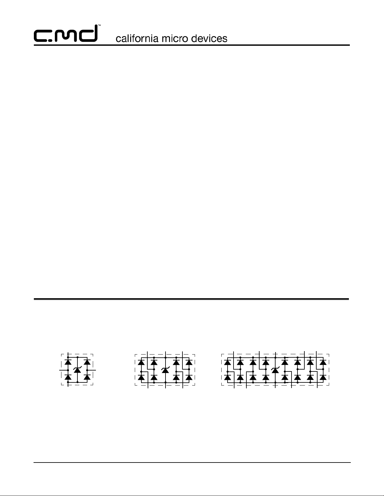
Electrical Schematics
CH6
V
P
CH1
V
N
CM1293-02ST/SO
CM1293--02SR
© 2006 California Micro Devices Corp. All rights reserved.
01/26/06 490 N. McCarthy Blvd., Milpitas, CA 95035-5112 ● Tel: 408.263.3214 ● Fax: 408.263.7846 ● www.cmd.com 1
CH2
CH4
CH1
CM1293-04ST/SO
CM1293-04MS/MR
CH3
V
P
CH2
V
N
CH8
CH1
CH7
CH2
CM1293-08MS/MR
V
P
CH3
V
N
CH5
CH4
Page 2
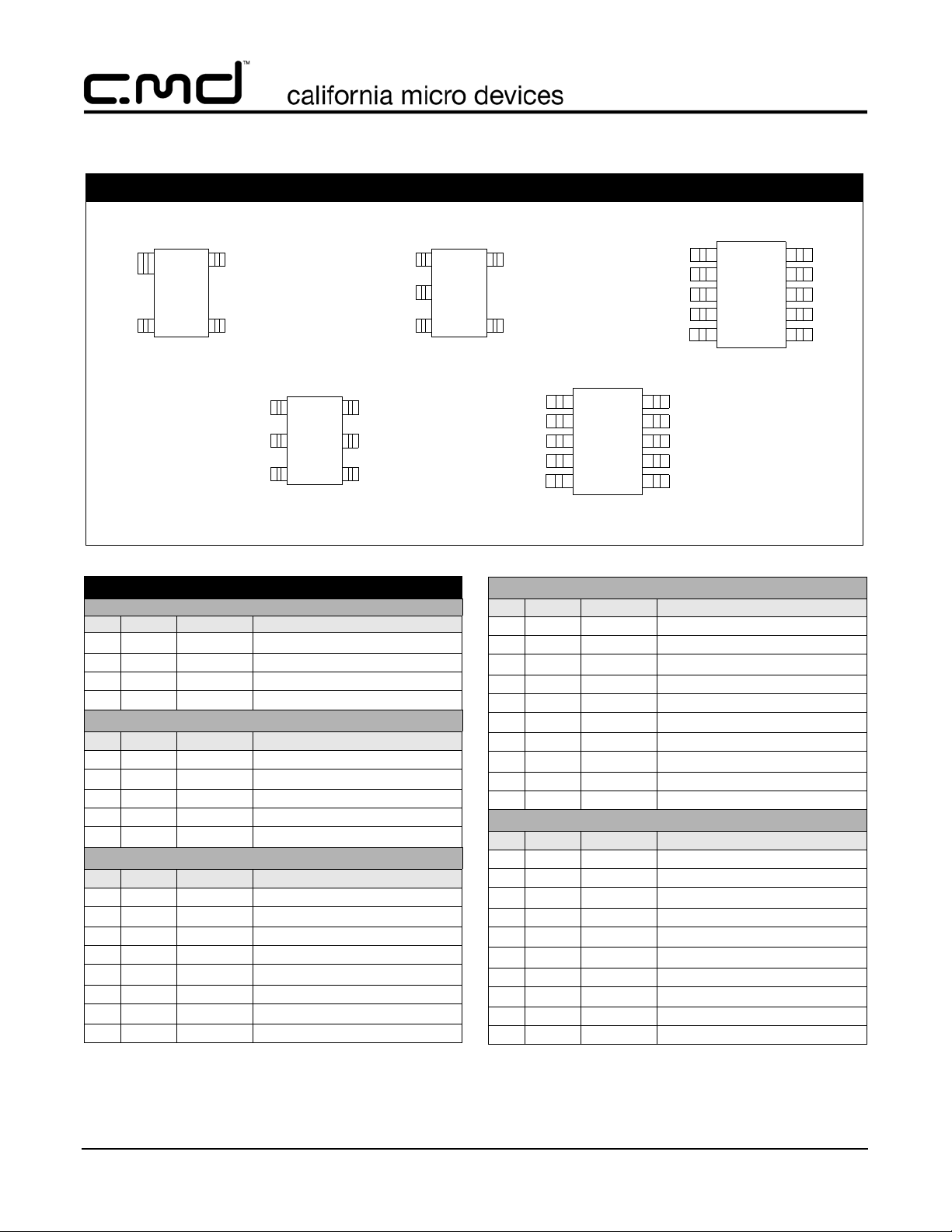
PACKAGE / PINOUT DIAGRAMS
CM1293
Top View
4
V
CH1
1
N
D036
2
V
P
3
CH2
4-Lead SOT143-4
Top View
CH1
CH2
1
D035
V
2
N
3
6-Lead SOT23-6
6
D034 /
5
4
Note: These drawings are not to scale.
PIN DESCRIPTIONS
2-CHANNEL, 4-LEAD SOT143-4 PACKAGE
PIN NAME TYPE PIN
V
1
2 CH1 I/O 2
3 CH2 I/O 3
4
PIN NAME TYPE DESCRIPTION
1 NC No connect
2V
3 CH1 I/O ESD Channel
4 CH2 I/O ESD Channel
5V
PIN NAME TYPE DESCRIPTION
1 CH1 I/O ESD Channel
2V
3 CH2 I/O ESD Channel
4 CH3 I/O ESD Channel
5V
6 CH4 I/O ESD Channel
5V
6 CH4 I/O ESD Channel
N
V
P
N
P
N
P
P
GND 1
PWR
2-CHANNEL, 5-LEAD SOT23-5 PACKAGE
GND Negative voltage supply rail
PWR Positive voltage supply rail
4-CHANNEL, 6-LEAD SOT23-6 PACKAGE
GND Negative voltage supply rail
PWR Positive voltage supply rail
PWR Positive voltage supply rail
Top View
1
NC
2
V
N
CH1
3
5-Lead SOT23-5
D032 /
D033
5
V
P
4
CH2
CH1
CH2
CH3
CH4
V
Top View
1
2
3
4
N
56
10-Lead MSOP-10
D039
10
D038 /
CH8
9
CH7
V
8
7
P
CH6
CH5
Top View
1
CH4
V
P
CH3
CH1
NC
V
CH2
P
10
2
D040 /
D041
3
4
56NC CH3
10-Lead MSOP-10
4-CHANNEL, 10-LEAD MSOP-10 PACKAGE
PIN NAME TYPE DESCRIPTION
1 CH1 I/O ESD Channel
2 NC No connect
3V
4 CH2 I/O ESD Channel
4
5 NC No connect
6 CH3 I/O ESD Channel
7 NC No connect
8V
9 CH4 I/O ESD Channel
10 NC No connect
PIN NAME TYPE DESCRIPTION
1 CH1 I/O ESD Channel
2 CH2 I/O ESD Channel
3 CH3 I/O ESD Channel
4 CH4 I/O ESD Channel
5V
6 CH5 I/O ESD Channel
7 CH6 I/O ESD Channel
8V
9 CH7 I/O ESD Channel
10 CH8 I/O ESD Channel
P
N
N
N
PWR Positive voltage supply rail
GND Negative voltage supply rail
8-CHANNEL, 10-LEAD MSOP-10 PACKAGE
PWR Positive voltage supply rail
GND Negative voltage supply rail
NC
CH4
9
V
8
7
N
NC
© 2006 California Micro Devices Corp. All rights reserved.
2 490 N. McCarthy Blvd., Milpitas, CA 95035-5112 ● Tel: 408.263.3214 ● Fax: 408.263.7846 ● www.cmd.com 01/26/06
Page 3
Ordering Information
PART NUMBERING INFORMATION
# of Channels Leads Package
2 4 SOT143-4 CM1293-02SR D036
2 5 SOT23-5 CM1293-02ST D032 CM1293-02SO D033
4 6 SOT23-6 CM1293-04ST D034 CM1293-04SO D035
4 10 MSOP-10 CM1293-04MS D040 CM1293-04MR D041
8 10 MSOP-10 CM1293-08MS D038 CM1293-08MR D039
Note 1: Parts are shipped in Tape & Reel form unless otherwise specified.
Specifications
Standard Finish Lead-free Finish
Ordering Part
Number
1
Part Marking
Ordering Part
Number
1
CM1293
Part Marking
ABSOLUTE MAXIMUM RATINGS
PARAMETER RATING UNITS
Operating Supply Voltage (V
Operating Temperature Range -40 to +85 °C
Storage Temperature Range -65 to +150 °C
DC Voltage at any channel input (V
- VN)6.0V
P
- 0.5) to (VP + 0.5) V
N
STANDARD OPERATING CONDITIONS
PARAMETER RATING UNITS
Operating Temperature Range -40 to +85 °C
Package Power Rating
SOT143-4 Package (CM1293-02SR)
SOT23-5 Package (CM1293-02ST/SO)
SOT23-6 Package (CM1293-04ST/SO)
MSOP-10 Package (CM1293-04MS/MR)
MSOP-10 Package (CM1293-08MS/MR)
225
225
225
400
400
mW
mW
mW
mW
mW
© 2006 California Micro Devices Corp. All rights reserved.
01/26/06 490 N. McCarthy Blvd., Milpitas, CA 95035-5112 ● Tel: 408.263.3214 ● Fax: 408.263.7846 ● www.cmd.com 3
Page 4
Specifications (cont’d)
CM1293
ELECTRICAL OPERATING CHARACTERISTICS
1
SYMBOL PARAMETER CONDITIONS MIN TYP MAX UNITS
V
I
V
I
LEAK
C
Operating Supply Voltage (VP-VN)3.35.5V
P
Operating Supply Current (VP-VN)=3.3V 8.0 μA
P
Diode Forward Voltage
F
Top Diode
Bottom Diode
IF = 8mA; TA=25°C
0.60
0.60
0.80
0.80
0.95
0.95
V
V
Channel Leakage Current TA=25°C; VP=5V, VN=0V ±0.1 ±1.0 μA
Channel Input Capacitance At 1 MHz, VP=3.3V, VN=0V, VIN=1.65V;
IN
2.0 pF
Note 2
ΔC
V
ESD
Channel I/O to I/O capacitance 1.5 pF
IO
ESD Protection
Peak Discharge Voltage at any
channel input, in system
a) Contact discharge per
Notes 2, 4 & 5; T
=25°C
A
±8
kV
IEC 61000-4-2 standard
b) Human Body Model,
MIL-STD-883, Method
Notes 2, 3 & 5; T
=25°C
A
±15
kV
3015
R
V
DYN
Channel Clamp Voltage
CL
Positive Transients
Negative Transients
Dynamic Resistance
Positive Transients
Negative Transients
At 8kV ESD HBM; TA=25°C; Notes 2 & 3
TA=25°C; Notes 5 & 6
+9.0
-9.0
1.2
0.6
V
V
Ω
Ω
Note 1: All parameters specified at TA = -40°C to +85°C unless otherwise noted.
Note 2: These parameters guaranteed by design and characterization.
Note 3: Human Body Model per MIL-STD-883, Method 3015, C
Note 4: Standard IEC 61000-4-2 with C
Note 5: These measurements performed with no external capacitor on V
Note 6: Measured under pulsed conditions, pulse width = 0.7mS, maximum current = 1.5A.
© 2006 California Micro Devices Corp. All rights reserved.
Discharge
= 150pF, R
Discharge
= 100pF, R
Discharge
= 330Ω, VP = 3.3V, VN grounded.
.
P
Discharge
= 1.5KΩ, VP = 3.3V, VN grounded.
4 490 N. McCarthy Blvd., Milpitas, CA 95035-5112 ● Tel: 408.263.3214 ● Fax: 408.263.7846 ● www.cmd.com 01/26/06
Page 5

CM1293
Performance Information (Cont’d)
Typical Filter Performance (nominal conditions unless specified otherwise, 50 Ohm Environment)
Figure 1. Insertion Loss (S21) VS. Frequency (0V DC Bias, V
Figure 2. Insertion Loss (S21) VS. Frequency (2.5V DC Bias, V
=3.3V)
P
=3.3V)
P
© 2006 California Micro Devices Corp. All rights reserved.
01/26/06 490 N. McCarthy Blvd., Milpitas, CA 95035-5112 ● Tel: 408.263.3214 ● Fax: 408.263.7846 ● www.cmd.com 5
Page 6

Application Information
Design Considerations
CM1293
In order to realize the maximum protection against
ESD pulses, care must be taken in the PCB layout to
minimize parasitic series inductances on the Supply/
Ground rails as well as the signal trace segment
between the signal input (typically a connector) and the
ESD protection device. Refer to Figure 3, which illustrates an example of a positive ESD pulse striking an
input channel. The parasitic series inductance back to
the power supply is represented by L
age V
where I
on the line being protected is:
CL
VCL = Fwd voltage drop of D1 + V
+ L
x d(I
2
is the ESD current pulse, and V
ESD
ESD
) / dt
and L2. The volt-
1
+ L1 x d(I
SUPPLY
) / dt
ESD
SUPPLY
is
the positive supply voltage.
An ESD current pulse can rise from zero to its peak
value in a very short time. As an example, a level 4
contact discharge per the IEC61000-4-2 standard
results in a current pulse that rises from zero to 30
Amps in 1ns. Here d(I
ΔI
/Δt, or 30/(1x10-9). So just 10nH of series induc-
ESD
tance (L
ment in V
and L2 combined) will lead to a 300V incre-
1
!
CL
)/dt can be approximated by
ESD
Similarly for negative ESD pulses, parasitic series
inductance from the V
pin to the ground rail will lead
N
to drastically increased negative voltage on the line
being protected.
The CM1293 has an integrated Zener diode between
V
and VN. This greatly reduces the effect of supply rail
P
inductance L
on VCL by clamping VP at the break-
2
down voltage of the Zener diode. However, for the lowest possible V
, especially when VP is biased at a
CL
voltage significantly below the Zener breakdown voltage, it is recommended that a 0.22μF ceramic chip
capacitor be connected between VP and the ground
plane.
As a general rule, the ESD Protection Array should be
located as close as possible to the point of entry of
expected electrostatic discharges. The power supply
bypass capacitor mentioned above should be as close
to the V
pin of the Protection Array as possible, with
P
minimum PCB trace lengths to the power supply,
ground planes and between the signal input and the
ESD device to minimize stray series inductance.
Additional Information
See also California Micro Devices Application Note
AP209, “Design Considerations for ESD Protection”, in
the Applications section at www.calmicro.com.
V
P
0.22μF
V
N
D
1
D
2
ONE
CHANNEL
OF
CM1213
2
PATH OF ESD CURRENT PULSE I
L
1
CHANNEL
INPUT
25A
0A
POSITIVE SUPPLY RAIL
LINE BEING
PROTECTED
V
CL
GROUND RAIL
ESD
CHASSIS GROUND
SYSTEM OR
CIRCUITRY
BEING
PROTECTED
V
CC
L
Figure 3. Application of Positive ESD Pulse between Input Channel and Ground
© 2006 California Micro Devices Corp. All rights reserved.
6 490 N. McCarthy Blvd., Milpitas, CA 95035-5112 ● Tel: 408.263.3214 ● Fax: 408.263.7846 ● www.cmd.com 01/26/06
Page 7

Mechanical Details
SOT143 Mechanical Specifications
Dimensions for CM1293-02SR devices supplied in 4pin SOT143 packages are presented below.
For complete information on the SOT143, see the California Micro Devices SOT143 Package Information
document.
PACKAGE DIMENSIONS
Package SOT143
Pins 4
Dimensions
A 0.80 1.22 0.031 0.048
A1 0.05 0.15 0.002 0.006
b 0.30 0.50 0.012 0.019
b2 0.76 0.89 0.030 0.035
c 0.08 0.20 0.003 0.008
D 2.80 3.04 0.110 0.119
E 2.10 2.64 0.082 0.103
E1 1.20 1.40 0.047 0.055
e 1.92 BSC 0.075 BSC
e1 0.20 BSC 0.008 BSC
L 0.4 0.6 0.016 0.024
L1 0.54 REF 0.021 REF
# per tape
and reel
Controlling dimension: millimeters
Millimeters Inches
Min Max Min Max
3000 pieces
CM1293
Mechanical Package Diagrams
TOP VIEW
e
43
E
E1
12
e1
SIDE VIEW
D
A
b2
END VIEW
c
b
A1
L
L1
Package Dimensions for SOT143.
© 2006 California Micro Devices Corp. All rights reserved.
01/26/06 490 N. McCarthy Blvd., Milpitas, CA 95035-5112 ● Tel: 408.263.3214 ● Fax: 408.263.7846 ● www.cmd.com 7
Page 8

Mechanical Details (cont’d)
SOT23-5 Mechanical Specifications
Dimensions for CM1293-02ST/SO devices packaged
in 5-pin SOT23 packages are presented below.
CM1293
Mechanical Package Diagrams
For complete information on the SOT23-5 package,
see the California Micro Devices SOT23 Package
Information document.
PACKAGE DIMENSIONS
Package SOT23-5 (JEDEC name is MO-178)
Pins 5
Dimensions
A -- 1.45 -- 0.0571
A1 0.00 0.15 0.0000 0.0059
b 0.30 0.50 0.0118 0.0197
c 0.08 0.22 0.0031 0.0087
D 2.75 3.05 0.1083 0.1201
E 2.60 3.00 0.1024 0.1181
E1 1.45 1.75 0.0571 0.0689
e 0.95 BSC 0.0374 BSC
e1 1.90 BSC 0.0748 BSC
L 0.30 0.60 0.0118 0.0236
L1 0.60 REF 0.0236 REF
# per tape
and reel
Controlling dimension: millimeters
Millimeters Inches
Min Max Min Max
3000 pieces
TOP VIEW
e1
e
54
E1
12 3
b
SIDE VIEW
D
A1
END VIEW
c
L1
L
E
A
© 2006 California Micro Devices Corp. All rights reserved.
8 490 N. McCarthy Blvd., Milpitas, CA 95035-5112 ● Tel: 408.263.3214 ● Fax: 408.263.7846 ● www.cmd.com 01/26/06
Page 9

Mechanical Details (cont’d)
SOT23-6 Mechanical Specifications
CM1293-04ST/SO devices are packaged in 6-pin
SOT23 packages. Dimensions are presented below.
For complete information on the SOT23-6 package,
see the California Micro Devices SOT23 Package
Information document.
CM1293
Mechanical Package Diagrams
TOP VIEW
e1
e
65 4
PACKAGE DIMENSIONS
Package SOT23-6 (JEDEC name is MO-178)
Pins 6
Dimensions
A -- 1.45 -- 0.0571
A1 0.00 0.15 0.0000 0.0059
b 0.30 0.50 0.0118 0.0197
c 0.08 0.22 0.0031 0.0087
D 2.75 3.05 0.1083 0.1201
E 2.60 3.00 0.1024 0.1181
E1 1.45 1.75 0.0571 0.0689
e 0.95 BSC 0.0374 BSC
e1 1.90 BSC 0.0748 BSC
L 0.30 0.60 0.0118 0.0236
L1 0.60 REF 0.0236 REF
# per tape
and reel
Controlling dimension: millimeters
Millimeters Inches
Min Max Min Max
3000 pieces
Pin 1
Marking
12 3
b
SIDE VIEW
D
END VIEW
c
E1
A1
E
A
L1
L
Package Dimensions for SOT23-6.
© 2006 California Micro Devices Corp. All rights reserved.
01/26/06 490 N. McCarthy Blvd., Milpitas, CA 95035-5112 ● Tel: 408.263.3214 ● Fax: 408.263.7846 ● www.cmd.com 9
Page 10

Mechanical Details (cont’d)
MSOP-10 Mechanical Specifications
CM1293-04MS/MR and CM1293-08MS/MR devices
are packaged in 10-pin MSOP packages. Dimensions
are presented below.
For complete information on the MSOP-10 package,
see the California Micro Devices MSOP Package Information document.
PACKAGE DIMENSIONS
CM1293
Mechanical Package Diagrams
TOP VIEW
D
10 9 8 7
6
Package MSOP
Pins 10
Dimensions
A 0.75 0.95 0.028 0.038
A1 0.05 0.15 0.002 0.006
B 0.18 0.40 0.006 0.016
C 0.18 0.007
D 2.90 3.10 0.114 0.122
E 2.90 3.10 0.114 0.122
e 0.50 BSC 0.0196 BSC
H 4.76 5.00 0.187 0.197
L 0.40 0.70 0.0137 0.029
# per tape
and reel
Millimeters Inches
Min Max Min Max
4000
Controlling dimension: inches
SEATING
PLANE
C
H
A
L
Pin 1
Marking
1234
SIDE VIEW
B
END VIEW
E
5
A1
e
Package Dimensions for MSOP-10
© 2006 California Micro Devices Corp. All rights reserved.
10 490 N. McCarthy Blvd., Milpitas, CA 95035-5112 ● Tel: 408.263.3214 ● Fax: 408.263.7846 ● www.cmd.com 01/26/06
Page 11

 Loading...