

Page 1
GaAs FET CLY 5
________________________________________________________________________________________________________
D a t a s h e e t
*Power amplifier for mobile phones
*For frequencies from 400 MHz to 2.5 GHz
*Wide operating voltage range: 2.7 to 6 V
* P
at V
=3V, f=1.8GHz typ. 26.5 dBm
*High efficiency better 55 %
ESD: Electrostatic discharge sensitive device,
observe handling precautions!
Type Marking Ordering code
(taped)
CLY 5 CLY 5 Q62702-L90 G S D S SOT 223
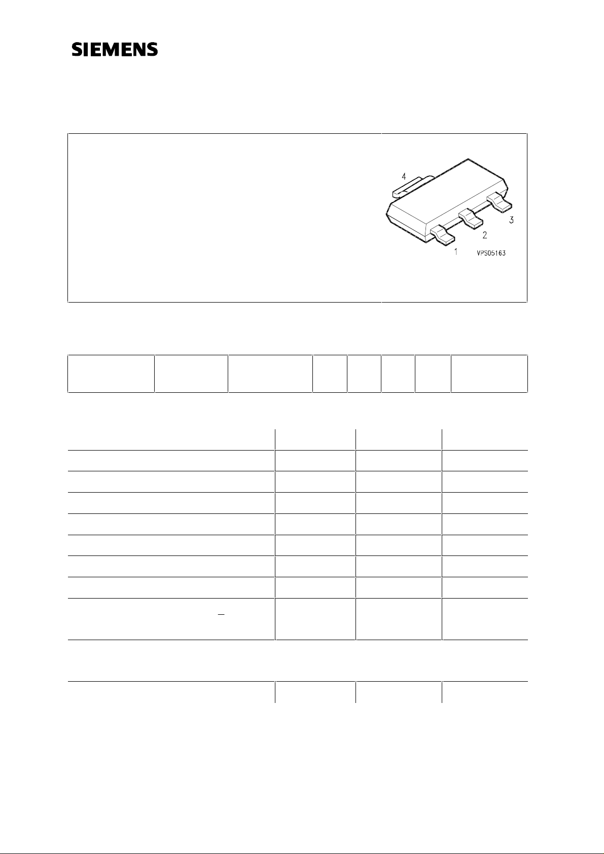
Pin Configuration
1 2 3 4
Package 1)
Maximum ratings Symbol Values Unit
Drain-source voltage V
Drain-gate voltage V
Gate-source voltage V
Drain current I
Channel temperature T
Storage temperature T
Pulse peak power P
Total power dissipation (T
Ts: Temperature at soldering point
< 80 °C)
s
Pulse
P
DS
DG
GS
D
Ch
stg
tot
9V
12 V
-6 V
1.2 A
150 °C
-55...+150 °C
9W
2W
Thermal Resistance
Channel-soldering point R
1) Dimensions see chapter Package Outlines
Siemens Aktiengesellschaft pg. 1/8 17.12.96
thChS
≤35
K/W
HL EH PD21
Page 2

GaAs FET CLY 5
________________________________________________________________________________________________________
Electrical characteristics (TA = 25°C , unless otherwise specified)
Characteristics Symbol min typ max Unit
Drain-source saturation current
V
DS
= 3 V
= 0 V
V
GS
Drain-source pinch-off current
V
DS
= 3 V
V
GS
= -3.8 V
Gate pinch-off current
V
DS
= 3 V
V
GS
= -3.8 V
Pinch-off Voltage
V
DS
= 3 V
=100µA
I
D
Small Signal Gain*)
= 3 V
V
DS
Pin = 0 dBm
= 350 mA f = 1.8 GHz
I
D
Small Signal Gain*)
= 5 V
V
DS
Pin = 0 dBm
= 350 mA f = 1.8 GHz
I
D
Small Signal Gain **)
= 3 V
V
DS
Pin = 0 dBm
= 350 mA f = 1.8 GHz
I
D
I
DSS
I
I
V
GS(p)
G
G
G
D
G
600 800 1200 mA
- 10 100 µA
-520µA
-3.8 -2.8 -1.8 V
10.5 11.0 - dB
11.5 12.0 - dB
p
9.0 9.5 - dB
Output Power
= 3 V
V
DS
Pin = 19 dBm
= 350 mA f = 1.8 GHz
I
D
Output Power
= 5 V
V
DS
Pin = 21 dBm
= 350 mA f = 1.8 GHz
I
D
1dB-Compression Point
V
DS
= 3 V
= 350 mA f = 1.8 GHz
I
D
1dB-Compression Point
V
DS
= 5 V
= 350 mA f = 1.8GHz
I
D
Power Added Efficiency
= 5 V
V
DS
Pin = 21 dBm
*) Matching conditions for maximum small signal gain (not identical with power matching conditions!)
**) Power matching conditions: f=1.8GHz:
Source Match: Γ
= 350 mA f = 1.8 GHz
I
D
: MAG 0.58; ANG -143°; Load Match: Γml : MAG 0.76; ANG -116°
ms
P
P
P
o
P
o
1dB
1dB
26.5 27 - dBm
29.5 30 - dBm
- 26.5 - dBm
- 30 - dBm
PAE 40 55 - %
Siemens Aktiengesellschaft pg. 2/8 17.12.96
HL EH PD21
Page 3
GaAs FET CLY 5
V
V
________________________________________________________________________________________________________
Compression Power vs. Drain-Source Voltage
f = 1.8GHz; IDS=0.5IDSS
P1dB
40
[dBm]
35
30
25
20
15
10
5
0
012345678
Drain-Source Voltage
[V]
ηη
D
80
[%]
70
60
50
40
30
20
10
0
Gain
16
[dB]
14
12
10
8
6
4
2
0
012345678
Drain-Source Voltage
P1dB
2.0
[W]
1.75
1.5
1.25
1.0
0.75
0.5
0.25
0
[V]
Output Characteristics
PtotDC
0,9
0,7
0,5
0,3
0,1
0
0123456
Drain-Source Voltage [V]
Siemens Aktiengesellschaft pg. 3/8 17.12.96
VGS = 0V
VGS = -0.5
VGS = -1V
VGS = -1.5
VGS = -2V
HL EH PD21
Page 4

GaAs FET CLY 5
________________________________________________________________________________________________________
typ. Common Source S-Parameters
VDS = 3 V ID = 350 mA Zo = 50 ΩΩ
f S11 S21 S12 S22
GHz MAG ANG MAG ANG MAG ANG MAG ANG
0,1 0,98 -26,6 11.52 160.7 0.01024 79 0.3 -171.8
0.15 0.96 -39.4 11.15 151.4 0.015 74.3 0.31 -169.3
0.2 0.93 -51.5 10.6 142.8 0.01942 69.9 0.33 -169.2
0.25 0.9 -63.1 10.06 134.9 0.02323 66.1 0.36 -169.4
0.3 0.87 -73.8 9.49 127.4 0.02665 62.3 0.38 -169.4
0.4 0.81 -93.3 8.34 114.1 0.03245 57 0.4 -172.7
0.5 0.77 -110.3 7.33 102.5 0.03711 52.8 0.43 -175.6
0.6 0.73 -125.3 6.47 92.4 0.04138 49.7 0.45 -179.4
0.7 0.71 -138.5 5.75 83.5 0.04528 47.3 0.47 177.5
0.8 0.7 -150.4 5.14 75.2 0.0489 45.2 0.49 174.2
0.9 0.69 -161.1 4.64 67.6 0.05271 43.3 0.5 170.8
1 0.68 -170.8 4.2 60.5 0.05646 41.6 0.51 168.1
1.2 0.69 172.1 3.51 47.2 0.06393 38 0.54 161.8
1.4 0.7 157.3 2.98 35.1 0.07181 34 0.57 155.6
1.5 0.71 150.5 2.76 29.2 0.07569 32 0.58 152.9
1.6 0.72 144.1 2.56 23.6 0.07941 29.7 0.59 149.4
1.8 0.74 132.2 2.22 12.6 0.08684 24.8 0.62 143.2
2 0.76 121.4 1.94 2.1 0.09377 19.7 0.65 137
2.2 0.78 111.5 1.7 -7.9 0.0998 14.6 0.68 130.9
2.4 0.8 102.5 1.49 -17.4 0.10532 9.4 0.7 124.7
2.5 0.81 98 1.39 -21.9 0.1076 6.7 0.71 121.1
3 0.85 79.2 1.01 -42.1 0.11638 -6 0.76 105.6
3.5 0.87 64 0.75 -58.1 0.12148 -17.2 0.8 91.4
4 0.89 51.4 0.59 -70.6 0.12571 -27.3 0.84 78.2
4.5 0.9 39.8 0.48 -82.2 0.12914 -37.2 0.86 65.6
5 0.92 29 0.41 -93.1 0.13429 -47 0.88 53.1
5.5 0.92 18.4 0.35 -103.4 0.13892 -57 0.9 40.3
6 0.92 8.3 0.31 -112.4 0.14142 -66.8 0.91 2 7
Siemens Aktiengesellschaft pg. 4/8 17.12.96
HL EH PD21
Page 5

GaAs FET CLY 5
________________________________________________________________________________________________________
typ. Common Source S-Parameters
VDS = 5 V ID = 350 mA Zo = 50 ΩΩ
f S11 S21 S12 S22
GHz MAG ANG MAG ANG MAG ANG MAG ANG
0.1 0.98 -26.3 13.02 160.1 0.00906 79.1 0.15 -153.9
0.15 0.95 -38.8 12.58 150.7 0.01326 73.7 0.17 -148.4
0.2 0.92 -50.8 11.98 141.9 0.01702 69.3 0.2 -148.5
0.25 0.89 -62.1 11.34 133.7 0.02026 65.6 0.23 -149.9
0.3 0.86 -72.6 10.68 126.1 0.02304 61.8 0.26 -150.6
0.4 0.8 -91.7 9.39 112.4 0.02771 57 0.29 -155.5
0.5 0.76 -108.3 8.24 100.6 0.03151 53.4 0.33 -159.4
0.6 0.72 -122.9 7.27 90.2 0.0348 51.2 0.35 -164.1
0.7 0.7 -135.9 6.45 80.9 0.03798 49.7 0.37 -167.6
0.8 0.69 -147.6 5.77 72.4 0.04099 48.8 0.4 -171.3
0.9 0.68 -158.1 5.2 64.5 0.04435 47.9 0.41 -174.9
1 0.68 -167.7 4.7 5 7 0.04784 47.1 0.44 -177.8
1.2 0.68 175.3 3.92 43 0.05543 45.2 0.47 175.4
1.4 0.7 160.4 3.31 30.1 0.06413 42.2 0.51 168.7
1.5 0.71 153.6 3.06 24 0.06865 40.6 0.54 165.5
1.6 0.72 147.1 2.83 17.9 0.07318 38.5 0.55 161.7
1.8 0.75 135 2.43 6.2 0.08237 33.7 0.6 154.6
2 0.77 123.9 2.1 -5 0.09121 28.3 0.64 147.5
2.2 0.8 113.7 1.82 -15.6 0.09917 22.5 0.67 140.4
2.4 0.82 104.3 1.58 -25.7 0.10617 16.7 0.7 133.3
2.5 0.83 99.7 1.47 -30.4 0.10916 13.6 0.72 129.1
3 0.87 80.1 1.02 -51.4 0.12055 -0.8 0.78 111.6
3.5 0.89 64.4 0.74 -67.4 0.12631 -13.4 0.83 95.8
4 0.91 51.5 0.56 -79.4 0.13053 -24.5 0.86 81.3
4.5 0.92 39.6 0.45 -90.2 0.13384 -35 0.88 67.9
5 0.93 28.8 0.37 -100 0.13894 -45.2 0.91 54.9
5.5 0.93 18.1 0.31 -109.2 0.1434 -55.5 0.92 41.7
6 0.93 8 0.27 -117.1 0.14538 -65.6 0.92 2 8
Additional S-Parameter available on CD
Siemens Aktiengesellschaft pg. 5/8 17.12.96
HL EH PD21
Page 6

GaAs FET CLY 5
________________________________________________________________________________________________________
Total Power Dissipation
P
Ptot
3.2
[W]
2.8
2.4
2.0
1.6
1.2
0.8
0.4
0
0 50 100 150
= f(Ts)
tot
Ts
O
C
Permissible Pulse Load
P
totmax/PtotDC
= f(tp)
Siemens Aktiengesellschaft pg. 6/8 17.12.96
HL EH PD21
Page 7

GaAs FET CLY 5
________________________________________________________________________________________________________
CLY5 Power GaAs-FET Matching Conditions
Definition:
ΓΓ
Measured Data:
Typ f
[GHz]
CLY5
Note: Gain is small signal gain @ Γms and Γ
0.9 3 350 25.8 15.6 0.50 133 0.70 -154
1.5 3 350 26.5 11.0 0.63 -167 0.74 -126
1.8 3 350 26.5 9.5 0.58 -143 0.76 -116
2.4 3 350 25.0 8.4 0.62 -108 0.68 -105
V
DS
[V]
5 350 29.2 16.3 0.52 144 0.61 -156
6 350 29.8 17.2 0.58 143 0.54 -168
5 350 30.0 11.5 0.59 -164 0.69 -126
6 350 30.6 12.6 0.64 -165 0.55 -132
5 350 30.0 10.0 0.56 -140 0.71 -118
6 350 30.5 10.0 0.58 -133 0.69 -119
5 350 29.1 8.7 0.60 -109 0.66 -105
6 350 30.5 8.9 0.65 -112 0.68 -106
I
D
[mA]
P-
1dB
[dBm]
ml
Gain
[dB]
Γ
ms
MAG
Γ
ms
ANG
Γ
ml
MAG
Γ
ml
ANG
Siemens Aktiengesellschaft pg. 7/8 17.12.96
HL EH PD21
Page 8

GaAs FET CLY 5
________________________________________________________________________________________________________
Increased Power Handling Capability Pulsed Applications
GSM/PCN TDMA-Frame:
577µs
Take value
4,615ms
P
tot
max
from diagram permissible pulse load -->
P
tot
DC
D =
t
p
==
T
P
tot
max
1.4
P
≈
tot
DC
ms
0577
4.615ms
0125..
P = 2W 1.4 = 2.8W
tot
DECT TDMA-Frame:
417µs
P
tot
Take value
max
P
from diagram permissible pulse load -->
tot
DC
10ms
×
D =
t
p
==
T
P
tot
max
1.5
P
tot
DC
10
4.615ms
≈
ms
00417.
P = 2W 1.5 = 3W
tot
Siemens Aktiengesellschaft pg. 8/8 17.12.96
×
HL EH PD21
 Loading...