

Page 1
®
CURRENT LIMITED OVER-VOLTAGE PROTECTED
APPLICATIONS
Industrial Automation
■
Programmable Logic Controller
■
Communication field bus nodes
■
Peripheral Input / Output modules
■
Machine tool interface
■
CLT3-4BT6
QUAD DIGITAL TERMINATION
FEATURES
4 channels topology
■
Wide range input DC Voltage:
■
VI= - 0.3 to 30V with RI=0
■
■ V
= - 30 to 35V with RI= 1.2kΩ
I
■ Low side configuration with common ground
Current limiter:
■
■ I
= 3mA
GEN
■ Input current limiter activation voltage < 5V
■
Temperature compensated operation
■
Opto-coupler drive:
■
No coupler activation below 1.5 mA input current
■
Input protection (RI= 1.2KΩ):
■
IEC61000-4-2 electrostatic discharge ESD, Class 3
❏
In contact, ±6kV; in air, ±8kV
❏
Level B: temporary disruption; no change of opto-coupler state
■
IEC61000-4-5 voltage surge, Class 3
❏
± 1000V with 42Ω serial resistor in differential mode
❏
Level B: temporary disruption
■
IEC61000-4-4 transient burst immunity
❏
± 4kV peak voltage; 5kHz repetitive rate
❏
Level A: fully functional
■
Operating ambient temperature: - 25 to 85°C
TSSOP20
BENEFITS
■
Reduced overall dissipation
■
Compact with high integration
■
Enables input to meet type 1 characteristic of IEC61131-2 standard
■
Compatible operation with 2 and 3 wires proximity sensor according EN60947-5-2 standard
■
Insensitive to the on state sensor impedance
■
Surface Mount Package for highly automated assembly
■
Enhanced functional reliability
August 2002 - Ed: 4A
1/10
Page 2
CLT3-4BT6
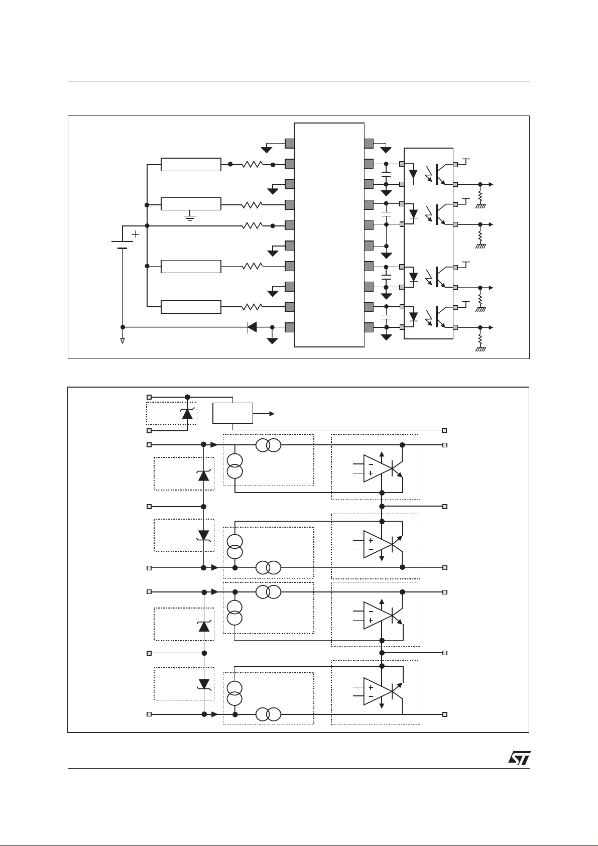
IEC61000-4 STANDARD ROBUST APPLICATION DIAGRAM
1
COM
V
IN
IN
1
1
1
ESD
IN
2
2
2
V
C
V
C
C
C
ESD
IN
3
COM
12
12
12
C
C
C
24V
SUPPLY
V
V
I
I
2 wires sensor
R
I
R
3 wires sensor
V
CC
I
R
C
R
I
Contact switch
COM
OUT
OUT
COM
COM
OUT
1
1
1
12
12
12
2
2
2
3
3
3
2 wires sensor
R
INPUT TERMINATION BLOCK DIAGRAM
Vc
BIASING
CIRCUIT
I
1
I
2
I
3
0.25xI
CURRENT LIMITER I
CURRENT LIMITER I
0.25xI
0.25xI
CURRENT LIMITER I
ESD
ESD
C
IN
1
12
IN
2
IN
3
ESD
Volt Prot
ESD
OVER
VOLTAGE
PROTECTION
ESD
OVER
VOLTAGE
PROTECTION
ESD
OVER
VOLTAGE
PROTECTION
I
TO COMPARATORS
0.75xI
LIM
LIM
LIM
0.75xI
LIM
0.75xI
LIM
LIM
ESD
IN
4
COM
LIM
LIM
LIM
COM
34
OUT
COM
OPTO COUPLER DRIVER
1.5mA
1.5mA
OPTO COUPLER DRIVER
OPTO COUPLER DRIVER
1.5mA
34
4
COM
OUT
1
I
1
COM
12
I
2
OUT
2
OUT
3
I
3
2/10
ESD
34
IN
4
ESD
OVER
VOLTAGE
PROTECTION
I
4
CURRENT LIMITER I
0.25xI
LIM
0.75xI
LIM
COM
34
LIM
1.5mA
I
4
OPTO COUPLER DRIVER
OUT
4
Page 3
CLT3-4BT6
FUNCTIONAL DESCRIPTION
TheCLTx-4isaquadruple input digitalterminationdevicedesignedfor 24 V DCautomationapplications.It
achieves the front-end circuitry of a digital input module (I/O) in industrial automation, and drives an
isolating opto-coupler.
Available in a four channels configuration, it offers a high-density termination by minimizing the external
components count. It is housed in a TSSOP20 surface mount package to reduce the printed board size.
Made of an input voltage protection, a serial current limiting circuit and an opto-coupler driver, each
channel circuit terminates the connection between the logic input and the associated high side sensor or
switch.
The CLT3-4 isa3mAquad channel device compatible the type 1 characteristics of the IEC61131-2
standard.
Each input voltage clamping block protects the module input against electromagnetic interferences such
as those described in the IEC61131-2 standard and IEC61000-4-2 (ESD), 4-4 (transient burst), 4-5
(voltage surge) standards. The supply input is also designed with such a protection structure.
The current limiting circuit connected between the input and the output pins is compensated all over the
temperature range. Thanks to its low tolerance, the current limitation allows reducing drastically the
dissipation of the input compared to a resistive input: the overall module requires less cooling capability
and becomes smaller.
The outputblockofeachterminationchannelcontrolstheoperationof anopto-coupler that is enabled by a
Light Emitting Diode.
When the input current is less than 1.5 mA, this output circuit derivates the input current to maintain the
opto-coupler off.
The original structure of the CLT limiter allows its activation threshold to be low and insensitive to the
output voltage up to a maximum value of 2.0 V.
When the CLT input voltage V
useof a reverse diodeand a serial resistor R
(3/4) is higher than 1.5 mA. The whole termination channel including the opto-coupler is on.
is higher than 5 V, or the module input voltage Vi higher than 11 V with the
IN
=1.2 kΩ, the outputcurrent that is a shareof the input current
I
ABSOLUTE RATINGS (limiting values)
Symbol Pin Parameter name & conditions Value Unit
V
CC
(1)
V
I
I
IN
V
C
IN Input steady state voltage, RI=0kΩ - 0.3 to 30 V
IN Input maximum forward current,
Supply steady state voltage, RC=0kΩ - 0.3 to 30 V
Supply steady state voltage, R
Input steady state voltage, R
Input repetitive pulse voltage, R
Input repetitive pulse voltage,
RI= 1.2kΩ,RC= 4.7kΩ
(2)
= 4.7kΩ - 0.3 to 35 V
C
= 1.2kΩ - 0.3 to 32 V
I
= 1.2kΩ - 0.3 to 35 V
I
-30to30 V
5mA
RI= 1.2kΩ,RC= 4.7kΩ
Input maximum reverse current,
RI= 1.2kΩ,RC= 4.7kΩ
V
OM
I
OM
T
AMB
T
J
Note 1: VI=VIN+RIxIIN;VIN= voltage at the input pin itself
Note 2: according to test diagramon figure 8, this case covers especially the reverse polarity operation of one input.
OUT Maximum output steady state voltage 2.5 V
OUT Output current - 4 to 4 mA
AII Operating ambient temperature - 25 to 85 °C
Operating and storage junction temperature - 25 to 150 °C
(2)
20 mA
3/10
Page 4

CLT3-4BT6
ELECTROMAGNETIC COMPATIBILITY RATINGS
= 1.2kΩ,RC= 4.7kΩ, reverse diode connected as shown on figure 6 (unless otherwise specified)
R
I
Symbol Node Parameter name & conditions Value Unit
V
PP
IN ESD protection, IEC61000-4-2, per input, in air ± 8 kV
ESD protection, IEC61000-4-2, per input, in contact ± 6 kV
ESD protection, IEC61000-4-2, per input, in air, R
ESD protection, IEC61000-4-2, per input, in contact, R
V
PPB
V
PP
V
PP
Note 3: test conditions of IEC standard applied to the application diagram page 2.
Note 4: see test circuit figure 6 or 7.
V
I
Total Peak Pulse Voltage Burst, IEC61000-4-4
CIN= 100pF, C
= 22nF, F = 5kHz (3)
OUT
VI Peak Pulse Voltage Surge, IEC61000-4-5, R = 42Ω, (4) ± 1 kV
V
CC
Peak Pulse Voltage Surge, IEC61000-4-5, R = 2Ω (4) ± 1 kV
=0Ω ±3 kV
I
=0Ω ±3 kV
I
±4 kV
THERMAL RESISTANCE
Symbol Parameter Value Unit
R
th (j-a)
TSSOP20 thermal resistance junction to ambient
90 °C/W
Board copper surface = 2cm², copper thickness = 35µm
ELECTRICAL CHARACTERISTICS
= 25°C, VCC= 24V and COM pin voltage referred unless otherwise specified)
(T
J
Symbol Pin Name Conditions Min. Typ. Max. Unit
Current limitation
I
LIM
IN Input limiting current V
= 0.9 to 2.0V
OUT
VIN=5to27V
T
= - 25 to 85°C
AMB
V
LOW
IN Maximum off state volt-
IIN= 100µA 1.5 V
age
V
TH
IN Activation threshold IIN= 2.1 mA 3.4 5 V
Input & Supply Protection
V
CL
IN Clamping voltage IIN= 7mA; tP=1ms 31 38 - V
Opto-coupler driver operation
V
I
OFF
OFF
I
ON
OUT Off state output current VI= 5V, (5) - 10 40 µA
I
= 1.5mA, (6) - 10 40 µA
IN
OUT Off state output voltage IIN= 1.5 mA 0.15 0.5 V
OUT On state output current VIN= 5V 1.5 2 - mA
Supply & biasing circuit
V
C
I
C
Note 5: According to application diagram on page 2 with use ofaRI=1.2kΩresistor, an opto-coupler (R
verse diode from COM to GND (VF= 0.7V)
Note 6: same as note 5 but RI=0Ω.
4/10
V
C
V
C
Supply voltage T
= - 25 to 85°C 10 V
AMB
Supply current VIN=VC= 30V 550 800 µA
2.1 3 3.7 mA
(0V)=15kΩ,VF=1.2V)and a re-
LED
Page 5

CLT3-4BT6
SWITCHING ELECTRICAL CHARACTERISTICS
= 25°C, VCC= 24V and COM pin voltage referred unless otherwise specified)
(T
J
Symbol Pin Name Conditions Min. Typ. Max. Unit
F
t
t
PLH
PHL
MAX
IN-OUT Input to output running frequency 200 Hz
IN-OUT Input activation propagation time C
IN-OUT Input de-activation propagation
time
INPUT CHARACTERISTICS OF CLT3-4
Fig. 1: Typical input characteristics of each CLT3-4 channel
V (V)
IN
30
30
25
20
15
10
5
5
2.1
= 22nF 6 µs
OUT
C
= 22nF 10 µs
OUT
3.7
0
0 0.5 1 1.5 2 2.5 3 3.5 4
Fig.2: Typical currentlimiter variation versusjunc-
tion temperature 0.9V < V
IIim / IIim (25°C)
102%
100%
98%
96%
94%
92%
90%
88%
86%
84%
-25 0 25 50 75 100 125
OUT
Tj (°C)
<2V
VIN= 27V
VIN= 5V
I (mA)IN
Fig. 3: Typical limiter threshold voltage variation
versus junction temperature for I
VTH (V)
3.6
3.5
3.4
3.3
Tj (°C)
3.2
-25 0 25 50 75 100 125
= 2.1mA
IN
5/10
Page 6

CLT3-4BT6
CLT3-4 INPUT / OUTPUT TRANSFER CHARACTERISTICS (respect to common pin COM)
Fig. 4: Current tranfer characteristic
I (mA)OUT
4
3.5
3
2.5
1.5
0.5
Forbidden
Transition zone
2
1
0.04
0
0 0.5 1 1.5 2 2.5 3 3.5 4
ISOLATOR OFF
I (mA)IN
ISOLATOR ON
2.1
Transition zone
3.7
Fig. 5: Transconductance characteristic
OUT
I (mA)
4
3.5
3
2.5
2
1.5
1
0.5
0
0 5 10 15 20 25 30
V (V)
I
ISOLATOR ON
APPLICATION DESCRIPTION
The CLT device is used between the connector and the opto-coupler of an I/O module. To secure the
coupler off state and the non-conduction of itsdiode, the maximum CLT output current is 40µA with R opto
= 15kΩ. When the CLT input voltage V
is higher than 5 V, a minimum CLT output current of 1.5 mA will
IN
secure the opto-coupler on state.
TheCLT limiter is insensitiveto the outputvoltage up to 2.0V.Therefore, its output isable to driveany state
of the art opto-coupler. Some additional device can be added in series with the opto-coupler if the output
voltage remains within its functional limits.
A stand-alone sensor is normally connected on the CLT input. For a good off state control, its quiescent
current has to be less than 1.5 mA (EN60947-5-2 standard compatible) keeping then the opto-coupler off
thanks to the CLT device (I
< 40µA). And its maximum ON state voltage V
OUT
will be lower than 8 V
S-ON
(EN60947-5-2standard compatible) corresponding to the difference between theminimum supply voltage
(V
I
IN MAX+VD(VI
=19.2V) and the maximumcurrent limitation activationvoltage V
CCMIN
= 11 V when VIN=5V,RI= 1.2 kΩ,IIN< 3.7 mA, VD= 1V).
CCMIN=VS-ON+VI;VI=VIN+RI
x
SURGE VOLTAGE TEST CIRCUIT
The input and supply pins are designed to withstand electromagnetic interferences. As shown on the
device block diagram, each channel input is protected by a clamping diode that is connected to the
commonpin COM. Combined with a serial inputresistance R
=1.2 kΩ, this clamping diode implements an
I
effective protection against transient voltage burst (±4 kV, IEC61000-4-4) and voltage surge (±1 kV,
IEC61000-4-5).
Thiscombination allows the surge voltage tobe applied from each inputto other inputs, the ground andthe
supply contacts in differential or common modes (see figure 6).
Thanks to its high resistance R
clamping diode such as the SM15T39C Transil™, the supply pin V
= 4.7 kΩ and the conventional power supply protection that uses a
C
withstands IEC61000-4-5 with +/-
C
1000 V surge voltage (see figure 7).
Finally, an external output capacitor may be placed in parallel with the opto-coupler diode to filter the
transient disturbances injected in the inputs of the module and secure the immunity of the opto-coupler
itself.
6/10
Page 7

CLT3-4BT6
Fig. 6: Input pin IN voltage surge test circuit.
V = ± 100V with 42PPΩ
V
CC
V
PP
I
V
PP
GND
PE/FE
5 nF
R
C
R
I
R
I
R
I
R
I
V
C
IN
IN
IN
IN
COM
1
2
3
4
CLT3-4
Fig. 7: Supply pin VCvoltage surge test cicuit.
V
C
IN
IN
IN
IN
COM
1
2
3
4
CLT3-4
± 1kV
42Ω
± 1kV
2Ω
CC
V
GND
PE/FE
SM15T39C
5 nF
R
C
R
I
R
I
R
I
R
I
INPUT REVERSE POLARITY ROBUSTNESS
Each input of the CLT device may be biased to a reverse polarity. This case corresponds to a connection
mistake or a reverse biasing that is generated by the demagnetization of a monitored inductive solenoid.
The involved input withstands the high reverse current up to 20 mA; its opto-coupler is OFF and protected
by the conducting input diode. The other inputs remain operational, and some extra dissipation is
generated in their clamping protections.
Considering the supply operation,a reverse blocking diode can be connected between the module ground
and the common pin COM to protect the CLT device against any spurious reverse supply connection.
Then, the whole module supply voltage rating is extended to ± 30V.
Fig. 8: Current sharing in the CLT device when IN4is biased at - 30V and the others at + 30V
C
V
I
V = 38 V
CL
4
REG N
I
REG4
OUT
OUT
N
4
OPTO
OPTO
N
4
CLT3-4
Vcc = + 30V
N
I = + 30V
N = 1,2 or 3
GND (0V)
4
I = -30V
1.1 mA
4.3 mA
1N4007
14 mA
4.7kΩ
IN
N
1.2kΩ
COM
1.2kΩ
IN
7/10
Page 8

CLT3-4BT6
Fig. 9: Typical junction to ambient thermal resis-
tance versus copper surface under common pad
(FR4 epoxy; copper thickness is 35µm).
th(j-a)(
R °C/W)
160
140
120
100
80
60
40
20
0
0.0 0.5 1.0 1.5 2.0 2.5 3.0 3.5 4.0 4.5 5.0
PIN-OUT CONNECTION
S(cm²)
The pins ESD, COM
COM
IN
ESD
12
IN
2
V
C
ESD
C
IN
3
ESD
34
IN
4
COM
, COM (pins # 1, 3, 6, 8, 10, 11, 13, 15, 16, 18, 20) must be connected together
IJ
10
1
2
3
4
5
6
7
8
9
20
19
18
17
16
15
14
13
12
11
COM
OUT
COM
OUT
COM
COM
OUT
COM
OUT
COM
1
12
2
3
34
4
externally. This common pad COM is enlarged to reduce the thermal resistance and improve the device
cooling. The COM and IN pins are designed to minimize the EMI effects on the circuit.
8/10
Page 9

TSSOP20 PRINTED BOARD EXAMPLE
CLT3-4BT6
COMMON PAD
GND COOLING PAD
ORDERING INFORMATION
Typical limited current
value, 3 = 3mA
COM
1
IN
ESD
12
IN
2
V
C
ESD
C
3
IN
ESD
34
IN
4
COM
CLT X - 4 B T6
EMC level
1000V according to IEC61000-4-5
COM
OUT
1
COM
12
OUT
2
COM
COM
OUT
3
COM
34
OUT
4
COM
Package
T6 = TSSOP20
Number of integrated channel
4 channels
OTHER INFORMATION
Ordering code Marking Package Weight Base qty Delivery mode
CLT3-4BT6 CLT3-4B TSSOP20 0.074 g 74 Tube
CLT3-4BT6-TR CLT3-4B TSSOP20 0.074g 2500 Tape & reel
■
Epoxy moulding resine meets UL 94,V0
9/10
Page 10

CLT3-4BT6
PACKAGE MECHANICAL DATA
TSSOP20
DIMENSIONS
REF.
Millimeters Inches
Min. Typ. Max. Min. Typ. Max.
A 1.200 0.047
A1 0.050 0.150 0.002 0.006
A2
A
b
D
20
e
11
E1
101
aaa
L1
L
k
A1
E
A2 0.800 1.000 1.050 0.031 0.039 0.041
b 0.190 0.300 0.007 0.012
c 0.090 0.200 0.003 0.007
D 6.400 6.500 6.600 0.252 0.256 0.259
E 6.200 6.400 6.600 0.244 0.252 0.256
E1 4.300 4.400 4.500 0.169 0.173 0.177
c
e 0.65 0.026
L 0.450 0.600 0.750 0.017 0.023 0.029
L1 1.000 0.039
k0°8°0°8°
aaa 0.100 0.004
TSSOP20 FOOTPRINT (in millimeters)
6.25
4.40 7.10
0.40
1.35
Informationfurnishedis believed to be accurate and reliable. However, STMicroelectronics assumes noresponsibilityforthe consequences of
useof such information nor for any infringement ofpatentsor other rights of third parties which mayresult from its use. No license is granted by
implication or otherwise under any patent or patent rights of STMicroelectronics. Specifications mentioned in this publication are subject to
change without notice. This publication supersedes and replaces all information previously supplied.
STMicroelectronics products are not authorized for use as critical components in life support devices or systems without express written approval of STMicroelectronics.
10/10
0.65
The ST logo is a registered trademark of STMicroelectronics
© 2002 STMicroelectronics - Printed in Italy - All rights reserved.
STMicroelectronics GROUP OF COMPANIES
Australia - Brazil - Canada - China - Finland - France - Germany
Hong Kong - India - Israel - Italy - Japan - Malaysia - Malta - Morocco - Singapore
Spain - Sweden - Switzerland - United Kingdom - United States.
http://www.st.com
 Loading...