

Page 1

®
CLP30-200B1
Application Specific Discretes
A.S.D™
OVERVOLTAGE & OVERCURRENT
PROTECTION FOR TELECOM LINE
MAIN APPLICATIONS
Any telecom equipment submitted to transient
overvoltages and lightning strikes such as :
Analog and ISDN line cards
■
PABX
■
DESCRIPTION
The CLP30-200B1 is designed to protect
telecommunication equipment. It provides both a
transient overvoltage protection and an
overcurrent protection.
The externalcomponents(balanced resistors, ring
relays contact, ...) needed by the CLP30-200B1
protection concept require very low power rating.
This results in a very cost effective protection
solution.
FEATURES
■
Dual bidirectional protection device.
■ High peak pulse current :
= 40A (5/310 µs SURGE)
I
PP
= 30A (10/1000 µs SURGE)
I
PP
■
Max. voltage at switching-on : 290V
■
Min. current at switching-off : 150mA
SO8
SCHEMATIC DIAGRAM (Top view)
TIPL
GND
1
TIPS
GND
BENEFITS
■
Voltage and current controlled suppression.
■
Surface Mounting with SO8 package.
■
Very low power rating of external components
on line card : balanced resistors, ring relay, low
voltage SLIC protection.
July 1999 - Ed: 4
GND
RINGL
GND
RINGS
1/11
Page 2
CLP30-200B1
Standard
Bellcore TR-NWT-1089
First level
Bellcore TR-NWT-1089
Second level
ITU-T-K20 / K21
ITU-T-K20
(IEC61000-4-2)
VDE0433
VDE0878
IEC61000-4-5
FCC Part 68, lightning
surge type A
Peak surge
voltage
(V)
2500
1000
Voltage
waveform
2/10µs
10/100µs
Required peak
current (A)
500
100
Current
waveform
2/10 µs
10/1000 µs
serial resistor to
5000 2/10 µs 500 2/10 µs 40
4000
1000
6000
8000
4000
2000
4000
2000
4000
2000
4000
1500
800
10/700 µs 100
5/310 µs 50
25
1/60 ns ESD contact discharge
ESD air discharge
10/700 µs 100
5/310 µs 50
50
1.2/50 µs 100
1/20 µs 22
50
10/700 µs
1.2/50 µs
1.2/50 µs
10/160 µs
10/560 µs
100
50
100
200
100
5/310 µs
8/20 µs
8/20 µs
10/160 µs
10/560 µs
Minimum
meet
standard (
20
25
0
0
0
5
0
50
0
22
17.5
12
)
FCC Part 68, lightning
surge type B
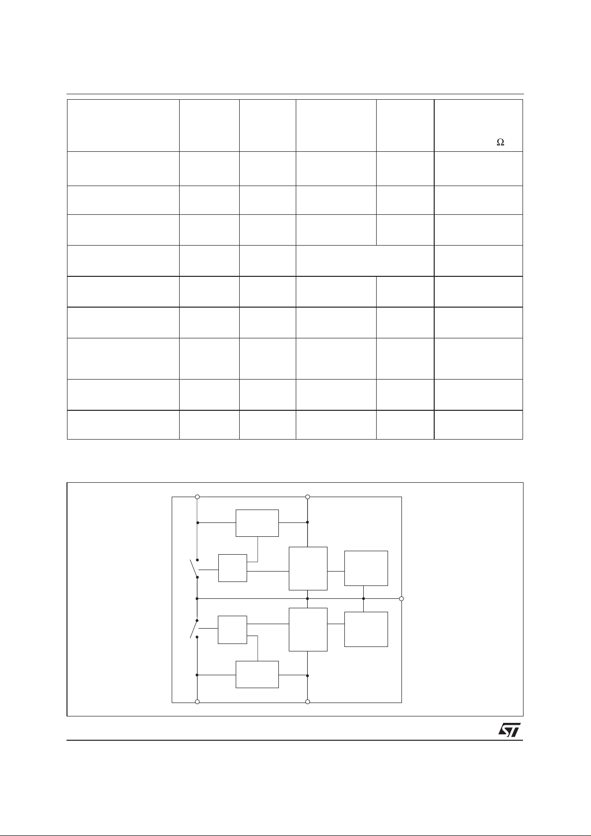
BLOCK DIAGRAM
1000 9/720 µs 25 5/320 µs 0
TIPL TIPS
Overcurrent
detector
OR
SW1
SW2
OR
Overcurrent
detector
RINGL RINGS
Overvoltage
detector
Overvoltage
detector
Overvoltage
reference
(> 200 V)
Overvoltage
reference
(> 200 V)
GND
2/11
Page 3
Pin Symbol Description
1 TIPL TIP (Line side)
2/3/6/7 GND Ground
4 RINGL RING(Line side)
5 RINGS RING(SLIC side)
8 TIPS TIP (SLIC side)
APPLICATION NOTE
CLP30-200B1
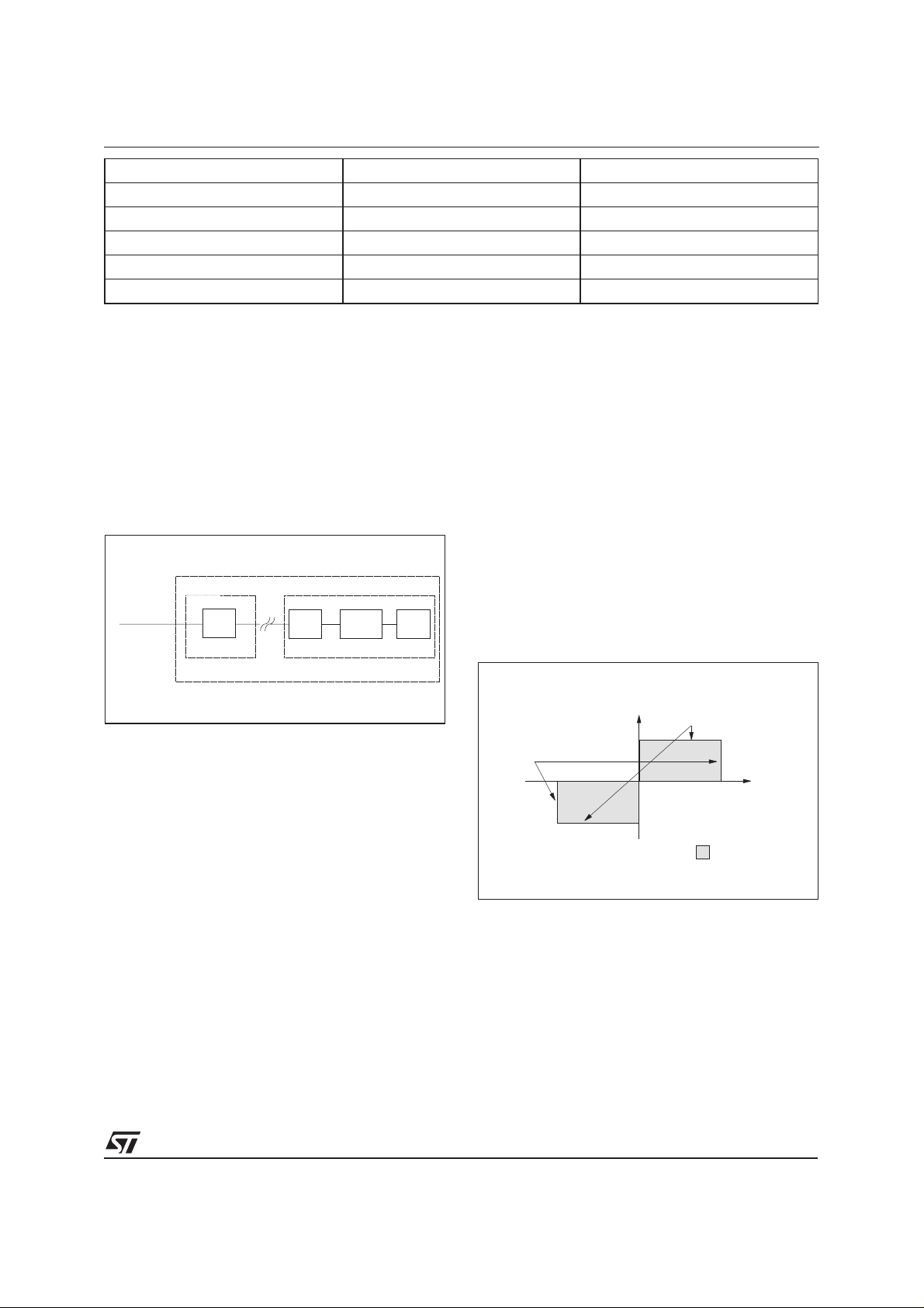
1.INTRODUCTION
The aim of this section is to show the behavior of
our new telecom line protection device.
Fig.1 : Suscriber line protection topology
telecommunication
"PRIMARY PROTECTION"
line
MDF LINE CARD
"SECONDARYPROTECTION"
CLP30200B1
EXCHANGE
VOLTAGE
REFERENCE
SLIC
Figure 1 is a simplified block diagram of a
subscriber line protection that is mainly used so
far.
This shows two different things :
■
A “primary protection” located on the Main Distribution Frame (MDF) eliminates coarsely the
high energy environmental disturbances (lightning transients and AC power mains disturbances) for which theITU-T-K20 requires a 4kV
10/700 µs test. This can be assumed either by
gas-tubes or silicon protection such as the
TLPxxM.
■
A “secondary protection” located on the line
card eliminates finely the remaining transients
that have not been totally suppressed by the
first stage. The ITU-T-K20 requires a 1 kV
10/700 µs test. At this stage, the protection is
managed by the CLP30-200B1.
2.STMicroelectronics CLP30-200B1CONCEPT
2.1 Evolution of the SLIC protection
Over the years, the performances of the SLICs
considerably increased and therefore the need of
the protection has also evolved.
The CLP30-200B1 is especially designed for the
protection of this new generation of SLIC. For this,
it is based on both overvoltage and overcurrent
protection modes.
Fig.2 : Line card protection
I
Programmable thanksto
an external resistor
+I
Programmable thanksto
any external voltage reference
-V
SWON
SWON
+V
-I
SWON
V
SWON
Line Card operating conditions
The figure 2 summarises the performance of the
CLP30-200B1 which basically holds the SLIC
inside its correct voltage and current values.
3/11
Page 4
CLP30-200B1
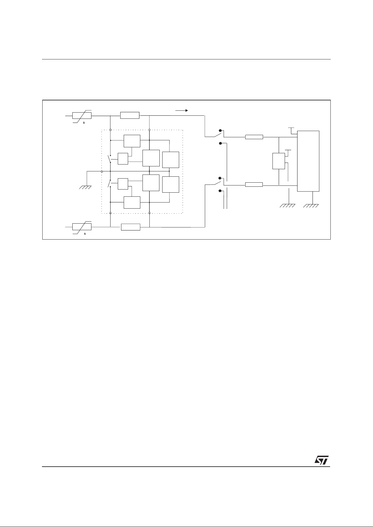
APPLICATION CIRCUIT : CLP30-200B1 in line card
Fig.3 : CLP30-200B1 in line card
PTC
TIP
R
GND
PTC
RING
R
R sense
R sense
TIPL TIPS
Overcurrent
detector
Overvoltage
detector
Overvoltage
detector
SW1
SW2
RINGL
OR
OR
Overcurrent
R sense
detector
RINGS
Overvoltage
reference
(> 200 V)
Overvoltage
reference
(> 200 V)
Figure above shows the topology of a protected
analog subscriber line at the line card side.
■ A first stage based on CLP30-200B1 manages
the high power issued from the external surges.
When used in ringing mode, the CLP30-200B1
operates in voltage mode and provides a
symmetrical and bidirectional overvoltage
protection above 200 V on both TIP and RING
lines. When used in speech mode, the
CLP30-200B1 operates in current mode and
the activation current of the CLP30-200B1 is
adjusted by R
■
A second stage which is the external voltage
SENSE
.
reference device defines the firing threshold
voltage during the speech mode and also
assumes a residual power overvoltage
suppression. This stage can be either a fixed or
programmable device such as LCP1511D.
I
External
voltage
reference
-Vbat
TIP
-Vbat
SLIC
RING
1
2
1
2
Ring
Generator
Rp
Rp
4/11
Page 5

2.3 Ringing mode
Fig.4 : Switching by voltage during ringing mode.
LG
I
TIP
GND
R sense
TIPL TIPS
Overcurrent
detector
Overvoltage
OR
SW1
detector
1/2 CLP200M
Overvoltage
reference
(>200V)
LG
V
CLP30-200B1
ILG
1
2
2
-200
1
3
A1
1
V
+200
LG
In ringing mode (Ring relay in position 2), the only
protection device involved is the CLP30-200B1.
In normal conditions, the CLP30-200B1 operates
in region 1 of A1 curve, and is idle.
If an overvoltage occurring between TIP (or RING)
and GND reaches the internal overvoltage
reference (+/- 200V), the CLP30-200B1 acts and
the line is short-circuited to GND. At this time the
operating point moves to region 2 for positive
surges (region 3 for negative surges). Once the
surge current disappears, the device returns to its
initial state (region 1).
Fig.5 : Methode to adjust the reference voltage.
TIP
R sense
TIPL TIPS
Overcurrent
detector
OR
SW1
SW2
OR
Overvoltage
detector
Overvoltage
detector
For surges occurring between TIP and RING, the
CLP30-200B1 acts in the same way. This means
that the CLP30-200B1 ensures a tripolar
protection.
When used alone, the CLP30-200B1 acts at the
internal overvoltage reference level (+/- 200 V).
Furthermore, it is possible to adjust this threshold
level to a lower voltage by using up to 4 fixed
external voltage reference (V
VZ1
Overvoltage
reference
(>200V)
Overvoltage
reference
(>200V)
GND
VZ2
VZ3
to VZ4) (see fig.5).
Z1
1
2
RING
RINGL
Overcurrent
detector
R sense
RINGS
VZ4
1
2
5/11
Page 6

CLP30-200B1
2.4 Speech mode
Fig.6 : Switching by current during speech mode.
I
LG
TIP
GND
R sense
TIPL TIPS
Overcurrent
detector
Overvoltage
OR
SW1
detector
Overvoltage
reference
(>200V)
1
2
V
LG
ILG
Rp
External
voltage
reference
-Vbat
-VBAT
6
4
5
V
LG
In speech mode (Ring relay in position 1), the
protection is provided by the combination of both
CLP30-200B1 and the external voltage reference
device (for example LCP1511D).
In normal conditions, the working point of this
circuit is located in region 4 of A2 curve :
the CLP30-200B1 is idle.
When a surge occurs on the line, the external
voltage reference device clamps at GND or -V
bat
respectively for positive and negative surges. This
generates a current which is detected by R
SENSE
and causes the protection to act : the line is
short-circuited to GND. The operating point moves
to region 6 for positive surges or region 5 for
negative surges.
Once the surge current falls below the
switching-off current I
, the CLP30-200B1
SWOFF
returns to its initial state (region 4).
Furthermore, the CLP30-200B1 switches when an
overvoltage, either positive or negative, occurs
either :
■ simultaneously on both TIP and RING lines
versus GND.
■
between TIP and RING.
■
on TIP (or RING) versus GND.
6/11
Page 7

CLP30-200B1
The choice of the switching-on current is function of the R
Fig . 7a and 7b : Switching-on current versus R
Iswon negative surge ( mA )
1000
100
1.6 3 6
Iswon - @ 0°C Iswon - @ +25°C Iswon - @ +70°C
Rsense ( Ohms )
SENSE
1000
resistors.
SENSE
Iswon @ 25°C ( mA )
Iswon + min Iswon + max Iswon - min Iswon - max
100
1.6 3 6
Rsense ( Ohms )
This current (typically above 150 mA) should not activate the protection device CLP30-200B1.
Thereforethe levelof activationis tobe chosenjust belowthis limit(typically 200mA).This levelis adjusted
through R
Figures 7a and 7b enable the designers to choose the right R
Example: The choice of R
SENSE
.
value.
SENSE
=3Ωensures a negative triggering of -280 mA min and -380mA max.
SENSE
In this case, the positive triggering will be 220mA min and 320mA max.
Thanks to the CLP30-200B1 topology, the surge current in the line is reduced after it.
Because the remaining surge energy is low, the power ratings of RP, the relay contacts and the external
voltagereference devicemay be keptlow. Thisresultsin asignificant cost reductionfor thewhole system.
7/11
Page 8

CLP30-200B1
ABSOLUTE MAXIMUM RATINGS (R
SENSE
=3Ω,T
amb
= 25°C)
Symbol Parameter Value Unit
I
PP
I
TSM
T
stg
T
j
T
L
ELECTRICAL CHARACTERISTICS (R
Line to GND peak pulse current
10/1000 µs (open circuit voltage wave shape 10/1000 µs)
5/310 µs (open circuit voltage wave shape 10/700 µs)
Non repetitive surge peak on-state current
F=50Hz
t
Storage temperature range
Maximum junction temperature
Lead temperature for soldering during 10 s.
SENSE
= 3 Ω, and T
amb
= 25 °C)
=10ms
t
p
= 200 ms
p
=1s
t
p
30
45
8.5
4.5
3.5
-40 to +150
150
260 °C
Symbol Parameter Test condtions Min Max Unit
I
LGL
Line to GND leakage current VLG= 200 V
10 µA
Measured between TIP (or
RING) and GND
V
V
SWON
LG
Line to GND operating voltage
Line to GND voltage at SW1 or
SW2 switching-on
Measured at 50 Hz between TIPL
(or RINGL) and GND,one cycle
200 V
290 V
A
A
°C
I
SWOFF
Line to GND negative current
Refer to test circuit fig 9
150 mA
at SW1 or SW2 switching-off
I
SWON
C
Line current at SW1 or SW2
switching-on
Line to GND capacitance V
Positive surge
Negative surge
=0V V
LG
OSC
= 200mV
RMS
220
370
320
470
100 pF
F = 1MHz
THERMAL RESISTANCE
Symbol Parameter Value Unit
R
th(j-a)
Junction to ambient
170 °C/W
mA
8/11
Page 9

CLP30-200B1
Fig.8 : TEST CIRCUIT FOR I
PARAMETER : GO - NO GO TEST
SWOFF
TIPL or RINGL
R
-V
D.U.T.
- 48 V
BAT
=
GND
Surge
generator
This is a GO-NO GO test which allows to confirm the switch-off current (IH) level in functional test
circuit.
TEST PROCEDURE
- Adjust the current level at the I
- Fire the D.U.T with a surge current : I
value by short circuiting the D.U.T
SWOFF
= 10 A, 10/1000 µs
PP
- The D.U.T will come back to the off-state within a duration of 50 ms max.
Fig. 9 : Typical variation of switching-on current
(positive or negative) versus R
SENSE
resistor and
Fig. 10 : Variation of switching-on current versus
SENSE
at 25 °C.
R
junction temperature (see test condition Fig. 11).
Iswon negative surge ( mA )
1000
Iswon - @ 0°C Iswon - @ +25°C Iswon - @ +70°C
Iswon @ 25°C ( mA )
1000
Iswon + min Iswon + max Iswon - min Iswon - max
100
1.6 3 6
Fig. 11 : I
SWON
Rsense ( Ohms )
MEASUREMENT
- ISWON = l1 when the CLP30-200B1 switches on (l1 is
progressively increased using R)
- Both TIP and RING sides of the CLP30-200B1 are
checked
48 V
.
R
L
Rsense
TIPL TIPS
DUT
L RINGS
RING
I1
GND
-RL=10Ω
±
100
1.6 3 6
Rsense ( Ohms )
fig. 12 : Relative variation of switching-off current
versus junction temperature (for R
SENSE
3 and 10 Ω).
I [Tj°C] / I [25°C]SWOFF SWOFF
1.4
1.2
1
0.8
R
0.6
0.4
020406080
Temperature (°C)
between
9/11
Page 10

CLP30-200B1
Fig. 13 : Relative variation of switching-off current
versus R
I [Rsense] / I [4 ]SWOFF SWOFF Ω
(between 3 and 10 Ω).
SENSE
1.6
1.4
1.2
1.0
0.8
0.6
0.4
46810
Rsense ( )Ω
Fig. 15 : Relative variation of internal reference
voltage versus junction temperature (I
V
REF [Tj°C] / V [25°C]REF
1.10
1.05
=1mA).
LG
Fig. 14 : Relative variation of switching-on voltage
versus dV/dt with an external resistor of 3 Ω.
V
SWON / REFV
1.12
1.10
1.08
1.06
1.04
1.02
1.00
0.98
0.1 0.3 1 3 10 30 100 300 1000
dV/dt (V/µs)
Fig. 16 : Capacitance (TIP/GND) versus applied
voltage (typical values).
C (pF)
70
50
1.00
0.95
0.90
0.85
-40 -20 0 20 40 60
Tj (°C)
Fig. 17 : Surge peak current versus overload
duration (maximum values).
TSM
I (A)
10
8
6
4
2
0
0.01 0.1 1 10 100 1000
t(s)
30
20
10
1 2 3 5 10 20 30 50 100
V (V)R
10/11
Page 11

PACKAGE MECANICAL DATA
SO8 plastic
CLP30-200B1
DIMENSIONS
REF.
Millimetres Inches
Min. Typ. Max. Min. Typ. Max.
L
A
a2
b
8
e
e3
D
M
5
S
F
c1
C
a3
a
1
E
b
A 1.75 0.069
a1 0.1 0.25 0.004 0.010
a2 1.65 0.065
a3 0.65 0.85 0.025 0.033
1
b 0.35 0.48 0.014 0.019
b1 0.19 0.25 0.007 0.010
C 0.25 0.50 0.50 0.010 0.020
c1 45° (typ)
D 4.8 5.0 0.189 0.197
E 5.8 6.2 0.228 0.244
1
4
e 1.27 0.050
e3 3.81 0.150
F 3.8 4.0 0.15 0.157
L 0.4 1.27 0.016 0.050
M 0.6 0.024
S 8° (max)
MARKING
Ordering code Marking Package Weight Base qty Delivery mode
CLP30-200B1 CLP30 SO-8 0.08g 100 Tube
CLP30-200B1RL CLP30 SO-8 0.08g 2500 Tape & Reel
Informationfurnishedisbelieved to be accurate and reliable. However, STMicroelectronicsassumesnoresponsibility for the consequences of
useofsuchinformationnor for any infringement of patents or other rights of third partieswhichmayresultfromits use. No license is granted by
implication or otherwise under any patent or patent rights of STMicroelectronics. Specifications mentioned in this publication are subject to
change without notice. This publication supersedes and replaces all information previously supplied.
STMicroelectronics products are not authorized for use as critical components in life support devices or systems without express written approval of STMicroelectronics.
The ST logo is a registered trademark of STMicroelectronics
© 1999 STMicroelectronics - Printed in Italy - All rights reserved.
STMicroelectronics GROUP OF COMPANIES
Australia - Brazil - China - Finland - France - Germany - Hong Kong - India - Italy - Japan - Malaysia
Malta - Morocco - Singapore - Spain - Sweden - Switzerland - United Kingdom - U.S.A.
http://www.st.com
11/11
 Loading...