

Page 1

CLP200M
ApplicationSpecific Discretes
A.S.D.
OVERVOLTAGE AND OVERCURRENT
PROTECTION FOR TELECOM LINE
MAINAPPLICATIONS
Any telecom equipment submitted to transient
overvoltagesandlightningstrikes suchas:
Analogand ISDNline cards
PABX
MainDistribution Frames
Primaryprotection modules
DESCRIPTION
TheCLP200Mis designedtoprotecttelecommunicationequipment.It providesbothatransientovervoltageprotectionand an overcurrentprotection.
It is housedin a PowerSO-10
TM
package.
FEATURES
DUALBIDIRECTIONALPROTECTIONDEVICE.
HIGHPEAKPULSE CURRENT:
Ipp = 100A(10/1000µs SURGE)
MAX.VOLTAGEAT SWITCHING-ON: 290V
MIN.CURRENT AT SWITCHING-OFF : 150mA
FAILURESTATUSOUTPUTPIN
BENEFITS
Both primary and secondaryprotectionlevelsin
onedevice.
Voltageand current controlledsuppression.
SurfaceMountingwithPowerSO-10
TM
package.
Line card cost reduction thanks to the very low
power rating of external components required :
balanced resistors, ring relay, low voltage SLIC
protection.
PowerSO-10
SCHEMATICDIAGRAM
1
TIP
S
TIP
L
TIP
L
TIP
L
TABis connected to GND
TM
NCFS
RING
RING
RING
RING
S
L
L
L
COMPLIESWITH THEFOLLOWINGSTANDARDS :
CCITTK20: 10/ 700µs 4kV
5 / 310µs 100A
BELLCORETR-NWT-000974
10/ 1000µs 1kV
10/ 1000µs 100A
February 1998 Ed : 3
1/21
Page 2

CLP200M
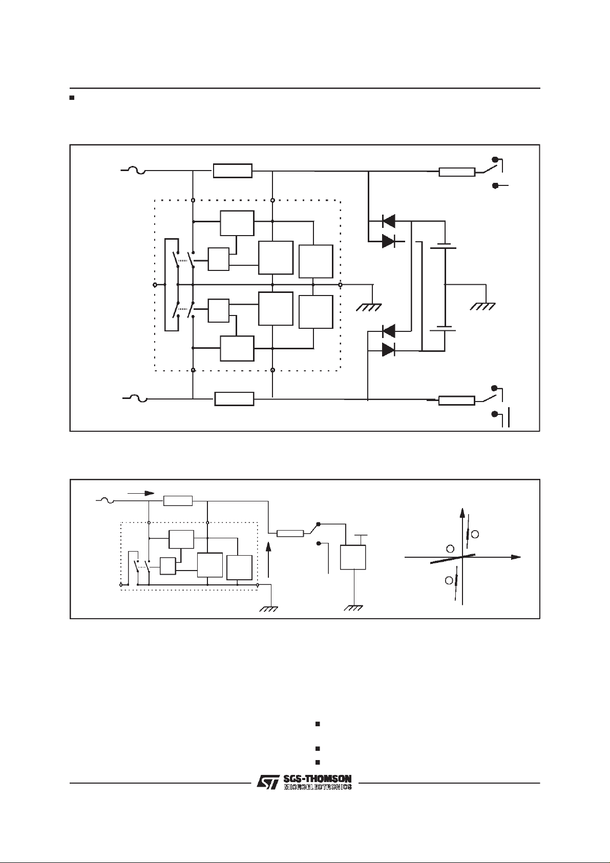
BLOCKDIAGRAM
TIPL TIPS
Overcurrent
detector
OR
SW3 SW1
FS GND
SW4 SW2
OR
Overcurrent
detector
RINGL RINGS
Overvoltage
detector
Overvoltage
detector
Overvoltage
reference
(+/- 215 V)
Overvoltage
reference
(+/- 215 V)
Pin Symbol Description
1 FS FailureStatus
2 TIPS TIP(SLICside)
3 / 4 / 5 TIPL
TIP(Lineside)
6 / 7 / 8 RINGL RING(Lineside)
2/21
9 RINGS RING(SLICside)
10 NC Not connected
TAB GND Ground
Page 3

APPLICATION NOTE
1. INTRODUCTION
The aim of this section is to show the behaviorof
ournewtelecomlineprotectiondevice.Thisdevice
includes a primary protection level and is suitable
for main distribution frames and line cards. This
protection concept is explained and, in addition,
the CLP200M performances are analysed when
facing different surgesas described in the CCITT
recommendations.
Fig.1 :
Subscriberline protectiontopology
telecommunication
line
”PRIMARYPROTECTION” ”SECONDARYPROTECTION”
MDF LINECARD
EXCHANGE
SLICCLP200M
CLP200M
2. SGS-THOMSONCLP200M CONCEPT
2.1Evolution of the SLIC protection
Over the years, the silicon protection performances have considerably changed .
The first generation of products like SMTHBTxx
and SMTHDTxx offered fixed overvoltage protection against surges on either TIP or RING line in
fourpackages.
The following generation like THBTxx and
THDTxx still offered fixed overvoltageprotection
againstsurgeson both TIP andRINGlines in two
packages.
The next step was the introduction of the
LCP1511D which brought the advantage of full
programmablevoltage.
Today, the CLP200M combines the features of all
the previous generations.In addition to that, it offers an overcurrent detection when operating in
speechmode and also a FailureStatusoutputsignal.
telecommunication
line
MDF LINECARD
”SECONDARYPROTECTION”
THDTxx or
EXCHANGE
LPC1511D
or LB200B
CLP200M SLIC
Figure 1 is a simplified block diagram of a subscriberline protectionthat ismainlyused sofar.
Thisshows two differentthings:
A ”primaryprotection”locatedon theMain DistributionFrame(MDF)eliminatescoarselythehigh
energy environmental disturbances (lightning
transientsand AC powermainsdisturbances)
A ”secondaryprotection”locatedon the line card
includesa primaryprotectionlevel(firststage)and
a residualprotection(secondstage)which eliminatesfinelytheremainingtransientsthathavenot
beentotallysuppressedby thefirststage.
The CLP200M can be used both in MDFs and in
line cards. In that case, any line card may be
swappedfrom one MDFtoanotherone withoutreducing the efficiency of the whole system protection.
The CCITT requirements are different for these
two protection locations (MDFs and line cards).
Concerningthe”primaryprotection”,theCCITTrequires a 4kV, 10/700µs surge test whereas the
”secondary protection” has to withstand a 1kV,
10/700µs surge test.
The explanations which follow are basically
coveringthelinecardapplication.
Fig. 2 :
Programmablethanks to
any external voltagereference
Linecard protection
I
+I
SWON
-I
Programmablethanks to
an external resistor
SWON
V
Line card operating conditions
The figure 2 summarizes the performance of the
CLP200MwhichbasicallyholdstheSLICinside its
correctvoltageandcurrentvalues.
3/21
Page 4

CLP200M
APPLICATION CIRCUIT : CLP200Min linecard
Fig.3 : CLP200Min line card
Fuse
TIP
RING
SW3 SW1
FS GND
SW4 SW2
Fuse
R sense
TIPL TIPS
Overcurrent
detector
Overvoltage
detector
Overvoltage
detector
RINGS
RINGL
OR
OR
Overcurrent
R sense
detector
Overvoltage
reference
(+/- 215 V)
Overvoltage
reference
(+/- 215 V)
I
1
Rp
2
1
Rp
2
Ring
Generator
External
voltage
reference
-Vbat
TIP
-Vbat
(*)
SLIC
RING
(*) LCP1511D orTHDT series
Figure 3 above showsthe topology of a protected
analog subscriber line at the exchange side. The
CLP200M is connected to the ring relay via two
balancedRp resistors, and to the SubscriberLine
Interface Circuit. A second device is located near
theSLIC : it canbe either a LCP1511Dor a THDT
series.
These two devices are complementary and their
functionsare explainedbelow:
The first stage based on CLP200M manages
the high power issued from the external
surges. When used in ringing mode, the
CLP200M operates in voltage mode and provides a symmetrical and bidirectional
overvoltage protection at +/-215 V on both TIP
and RING lines. When used in speech mode,
the CLP200M operates in current mode and
the activation current of the CLP200M is adjusted by R
SENSE
.
The second stage is the external voltage reference device which defines the firing threshold
voltage during the speech mode and also assumes a residual power overvoltage
suppression.This protectionstagecan be either
a fixed or programmable breakover device. The
THDTxxfamilyacts as a fixed breakover device
whilethe LCP1511Doperatesas a programmableprotection.
Thanks to this topology, thesurge current in the
line is reduced after the CLP200M. Because the
remainingsurgeenergyis low,thepowerratingsof
Rp,the ringrelaycontactsand theexternalvoltage
referencecircuit maybe downsized.This resultsin
a significantcostreduction.
4/21
Page 5

2.3 Ringingmode
Fig.4 : Switchingbyvoltage duringringingmode.
ILG
Fuse
TIP
FS
Rsense
TIPL TIPS
Overcurrent
detector
OR
SW3 SW1
Overvoltage
detector
1/2 CLP200M
Overvoltage
reference
(+/- 215 V)
VLG
GND
CLP200M
ILG
1
Rp
2
-215
3
A1
2
1
VLG
+215
In ringing mode (Ring relay in position 2), the only
protectiondeviceinvolvedis theCLP200M.
Innormalconditions,theCLP200Moperatesin region1 of A1 curve,andisidle.
If an overvoltageoccuringbetween TIP(or RING)
and GND reaches the internal overvoltage reference(+/- 215V),theCLP200Mactsand thelineis
short-circuited to GND. At this time the operating
pointmovestoregion2 for positive surges(region
3 for negativesurges).Oncethe surgecurrentdisappears, the device returns to its initial state (region1).
Fig.5a : Methodto adjustthereferencevoltage.
Fuse
TIP
SW3 SW1
R sense
TIPL TIPS
Overcurrent
detector
Overvoltage
OR
detector
For surges occuring between TIP and RING, the
CLP200M acts in the same way. This means that
theCLP200M ensuresa tripolarprotection.
Whenused alone, theCLP200M acts at the internalovervoltagereferencelevel(+/-215V).Furthermore,it is possible to adjust this thresholdlevel to
a lowervoltageby using :
.up to 4 fixed external voltage reference (V
V
) (seefig.5a).
Z4
1
Rp
2
VZ1
Overvoltage
reference
(+/- 215 V)
VZ2
Z1
to
RING
FS GND
Fuse
SW4 SW2
RINGL
OR
Overcurrent
detector
R sense
Overvoltage
detector
RINGS
Overvoltage
reference
(+/- 215 V)
VZ3
VZ4
1
Rp
2
5/21
Page 6
CLP200M
externalreferencesupplies,Vb1andVb2(seefig.5b)..
Fig. 5b: Methodto adjustthe referencevoltage.
TIP
RING
Fuse
R sense
TIPL TIPS
Overcurrent
detector
Overvoltage
OR
SW3 SW1
FS GND
Fuse
SW4 SW2
RINGL
OR
Overcurrent
R sense
detector
detector
Overvoltage
detector
RINGS
Overvoltage
reference
(+/- 215 V)
Overvoltage
reference
(+/- 215 V)
1
Rp
2
VB1
VB2
1
Rp
2
2.4 Speechmode
Fig.6 : Switchingby currentduring speechmode.
ILG
Fuse
TIP
FS
R sense
TIPL TIPS
Overcurrent
detector
OR
SW3 SW1
Overvoltage
detector
Overvoltage
reference
(+/- 215V)
VLG
GND
In speech mode(Ringrelayin position1),the protection is provided by the combination of both
CLP200M and the external voltage reference device.
In normal conditions, the working point of this circuit is located in region 4 of A2 curve : the
CLP200Mis idle.
Whena surgeoccurs on the line,theexternal voltage reference device clamps at GND or -V
bat
respectivelyforpositiveand negativesurges.
This generates a current which is detected by
R
andcausestheprotectiontoact: theline is
SENSE
short-circuitedto GND.
6/21
ILG
1
External
voltage
reference
-Vbat
-VREF2
5
4
VREF1
6
Rp
2
The operatingpoint moves to region 5 for positive
surgesor region6 fornegative surges.
Once the surge current falls below the switchingoff current I
, the CLP200M returns to its in-
SWOFF
itialstate (region 4).
Furthermore, the CLP200M switches when an
overvoltage, either positive or negative, occurs
either:
simultaneouslyon bothTIP and RING lines versusGND.
betweenTIP andRING.
onTIP (orRING)versus GND.
A2
V
LG
Page 7

CLP200M
Fig. 7a and 7b : Switching-on current versus
R
.
SENSE
ISWON (mA)
500
300
200
100
3 5 7 9 11 13
Iswon@ 25°C (mA)
500
300
200
100
357911
-20°C25°C75°C
Rsense ( )Ω
Iswonmin Iswon max Iswonmin Iswonmin
negative negative positive positive
Rsense ( )Ω
The choice of the switching-on current is function
oftheR
SENSE
resistors.
In normal operating condition, only the negative
currentofthesignalisof interest.Thiscurrent(typically below -150 mA) should not activate the protection device CLP200M. Therefore the level of
activationis to be chosenjustabove thislimit (typically -200 mA). This level is adjusted through
SENSE
.
R
Figures7a and 7b enablethe designersto choose
theright R
SENSE
value.
2.5. FailureStatus
The CLP200M has an internal feature that allows
the user to get a Failure Status (FS) indication.
When the CLP200M is short-circuiting the line to
GND,a signalcanbemanagedthrough pin 1.This
signalcan beusedto turna LEDon inordertoprovide a surge indication. It mayalsobe used with a
logic circuitryto count the number of disturbances
appearingon the lines.
Fig. 8 : FailureStatus circuit anddiagnostic.
Rsense
1
FAILURE
STATUS
1k
+12V
CLP200M
Rsense
If a surge exceeding the maximum ratings of the
CLP200Moccurson the line, the devicewill fail in
a short-circuit state.
Fig.9 :
Operationlimitsanddestructionzoneof the
CLP200M.
Ipp (A)
1000
100
10
0.01 0.1 1 10
t (ms)
EXAMPLE :
The choice of R
=4Ωensures a negative
SENSE
triggeringof -220mAmin and-320mAmax.In this
case,thepositivetriggeringwillbe 180mAminand
280mAmax.
Thefigure 9 showstwo differentcurves:
Theloweroneindicatesthe maximumguaranted
workinglimits of the CLP200M.
Theupper curveshowsthelimit abovewhichthe
CLP200Miscompletelydestructed. Inthiscase,
theFail Diagnosticpin is on.
7/21
Page 8

CLP200M
3. CLP200MTESTSRESULTSACCORDINGTO
CCITTK20RECOMMENDATIONS
3.1CCITT K20 Recommendations
In respect with the CCITT recommendations, the
CLP200M has to withstand three kinds of disturbances.
3.1.1. Lightning simulation
(Test2, table2/K20)
Thistest shallbe donein transversaland longitudinalmodesas shown in figure10.
Fig.10 : Transversaland longitudinaltest
topologies.
AorB
ITEM
UNDER
BorA
TEST
E
A
25
25
ITEM
UNDER
B
TEST
E
4kv
4kv
15 25
0.2µF5020µF
TRANSVERSAL TEST
15
0.2µF5020µF
Fig. 11 :
Powerinduction testcircuit.
1µF
S2
1µF
100
S1
R1
R2
A
ITEM
UNDER
TEST
B
E
3.1.3.Powercontact(Test 3, table1/K20)
Thistest shall be donewith the testcircuitof figure
12.
Vac(max)= 220V
, with switchS in each posi-
RMS
tionand duration 15 min.
Fig. 12 : Powercontact testcircuit.
<10
600
<10
600
A
UNDER
B
ITEM
TEST
E
LONGITUDINAL TEST
The test generator is the 10/700µs with 4kV of
peakvoltage.
3.1.2. Powerinduction
(Test3a and3b, table2/K20)
Twokinds of testsusing thesame circuittopology
(seefig.11) are definedin the CCITTK20.
Test3a :
Vac(max)= 300V
, R1= R2= 600
RMS
Ω
S2operatingand test duration= 200ms.
Test3b :
Vac(max)= 300V
(*),R1 = R2 = 200Ω
RMS
S2operatingand test durationnot defined.
(*)Recommended value.
8/21
3.1.4.Acceptance criteriaand numberof tests
Forthetestsdescribedin chapter3.1.1.,3.1.2.and
3.1.3.two criteria aredefined:
A:Equipmentshallwithstandthetestwithoutdam-
ageand shalloperateproperly withinthespecified
limits.
B:A fire hazard shouldnot occur in the equipment
asa resultof thetests.
The criteria are affected to the different tests as
mentionedin the table 1.
Page 9

CLP200M
Table1 : Acceptancecriteriaand numberof tests.
TEST ACCEPTANCE
NUMBERTO TESTS
CRITERIA
2 A 10 forlongitudinalA
10 forlongitudinalB
and 10 fortransversal
3a A 5
3b B 1
3 B 1 foreach positionof s
3.2.Ringingmode
3.2.1. Lightningsimulationtest
Lightningphenomenaare themostcommon surge
causes.The purpose of thistest isto checkthe robustnessof the CLP200M against these lightning
strikes.
Fig.13 : Lightningsimulationtest.
10/700µs
I
GENERATOR
+/- 4kV
Rsense
TIPL
1/2 CLP200M
GND
4Ω
TIPS
Rp
V
Fig.15 :
CLP200Mresponseto a negativesurge.
Figures 14 and 15 show that the remaining overvoltagedoesnot exceed+/- 260V. The CLP200M
switcheson within0.7µsandwithstandsthe 100A
givenby theCCITTK20 generator.
Consequently,the CLP200Mtotally fulfillsthistest.
3.2.2Power induction
(Test3a and 3b table2/K20)
Surgesof longdurationwithmediumvoltagevalue
are mainly produced by the proximity of a subscriber line with an AC mains line or equipment.
Thepurpose of this testisto checkthe robustness
ofthe CLP200Magainst these capacitivecoupling
disturbances.
Fig. 16 : Powerinductancetest.
Fig.14 :
CLP200Mresponseto a positivesurge.
TEST V
(RMS)
R(Ω) Duration
3a 300 600 0.2s
3b 300 200 ?
9/21
Page 10

CLP200M
Fig. 17 : CLP200Mresponseto the induction test
(Test3a).
Fig. 18 : CLP200M reponse to the induction test
(Test3b).
The test 3 of CCITT K20 requiresa serial PTC (or
fuse)which is insertedin the test circuit to limit the
currentrate. ThisPTCactslikean open-circuitin a
non-instantaneous way when a surge occurs on
the line. Meanwhile, the CLP200M has to withstandthe surge.
Fig.19 : Powercontact test.
600 < 10ΩΩ
or
15min
V(RMS)
50Hz
I
PTC
4
Rsense Rp
TIPL TIPS
1/2 CLP200M
GND
V
Fig. 20 : Powercontacttest 3 (With10Ωseries).
Figures17 and18 showthat theremainingvoltage
doesnotexceed 270 V.
Consequently,the CLP200Mtotally fulfillsthistest.
The test duration is not specified in test 3b. If the
duration exceeds 5s we do suggest to follow the
soldering and mounting recommendations given
onpage17ofthis document.
3.2.3Power contact(Test3 table1/K20)
This long duration surge is produced when connecting a subscriber line to an AC mains line or
equipment.Thepurposeof thistestis tocheckthe
robustnessof the CLP200M against these disturbances.
10/21
Figure 20 shows that the remaining overvoltage
does not exceed 250 V and shows that the PTC
actslike anopen-circuit after60 ms.
Consequently,the CLP200Mtotally fulfillsthistest.
3.3.Speechmode
3.3.1.Lightningsimulation test
(Test2, table2/K20)
Fig.21: Lightningtest in speechmode.
10/700µs
GENERATOR
+/- 4kV
I
1
4
Rsense
TIPL TIPS
1/2 CLP200M
GND
V1
I2
50
Rp
-48V
LCP1511D
SLIC
V2
Page 11

CLP200M
Fig.22 : CLP200Mresponseto a positivesurge.
Fig. 23 : CLP200Mresponseto a negativesurge.
3.3.2Power inductiontest
(Test3a and 3b, table 2/K20)
Fig.24 : Powerinductiontest.
I
1
V(RMS)
50 Hz
TEST V
TIPL
1/2 CLP200M
(RMS)
4Ω
Rsense
TIPS
GND
V1
R(Ω) Duration
I2
50
Rp
-48V
LCP1511D
SLIC
V2
3a 300 600 0.2s
3b 300 200 ?
Figures25 and26 showthat themaximumremaining voltage does not exceed +2V for positive
surgesand -55V for negativesurges.
Consequently,the CLP200Mtotally fulfillsthistest.
The test duration is not specified in test 3b. If the
duration exceeds 5s we do suggest to follow the
soldering and mounting recommendations given
onpage17of this document.
Figures22 and23 givethe voltageandcurrentbehaviorduringpositiveandnegative4kV,10/700µs,
surge tests using a LCP1511D as second stage
protection device. The firing threshold values are
now adjusted to GND and to -Vbat (-48V) by the
actionof thesecondstageprotectionwhichactsas
anexternalvoltage reference.
As shown on these figures, the maximumremaining voltage does not exceed +2.5V for positive
surgesand -60V for negativesurges.
Consequently,the CLP200Mtotally fulfillsthistest.
Fig.25 :
Inductiontest behavior(Test3a).
11/21
Page 12

CLP200M
Fig.26 : Inductiontest behavior(Test3b).
3.3.3- Powercontact test (Test3 table1/K20)
The test 3 of CCITT K20 requires a serial PTC (or
fuse)which isinsertedinthe test circuitto limit the
currentrate. This PTC acts like an open-circuitafter 60 mswhen a surge occurs on the line. Meanwhile,theCLP200Mhasto withstandthe surge.
The protection device CLP200M totally fulfills this
test.
Fig.28 :Powercontacttest3 (withR≤10Ωseries).
Fig. 27 : Power contacttest.
600 or < 10
12/21
V(RMS)
50Hz
I
PTC
15min
4Ω
Rsense Rp
TIPL TIPS
1/2 CLP200M
GND
I2
SLIC
-48V
V
LCP1511D
V2
Page 13

CLP200M
ABSOLUTEMAXIMUMRATINGS (R
SENSE
=4Ω, and T
Symbol Parameter Test Conditions Value Unit
I
PP
Line to GNDpeak surge
current
10/1000µs (open circuitvoltage
wave shape10/1000µs)
5/310µs(opencircuit voltage
wave shape10/700µs)
I
TSM
Mainspowerinduction
current
Mainspowercontact current V
V
=300V,R= 600Ω
RMS
t =200ms
=220V,R= 10Ω
RMS
(failurestatus threshold)
t =200 ms
= 220V,R =600
V
RMS
t =15 mn
T
stg
T
j
T
L
Storagetemperature range
Maximumjunctiontemperature
Maximumleadtemperatureforsolderingduring10 s
amb
=25°C)
Ω
100 A
130 A
0.5 A
22 A
0.30 A
- 40 to + 150
150
260 °C
°C
ELECTRICAL CHARACTERISTICS
(R
SENSE
=4Ω, andT
amb
=25°C)
Symbol Parameter Test Conditions
I
LGL
Line to GNDleakage
current
. VLG= 200V
.
MeasuredbetweenTIP
(orRING)and GND
V
ref
Overvoltageinternal
reference
.
=1mA
I
LG
.MeasuredbetweenTIP
(orRING)and GND
V
SWON
I
SWOFF
Line to GNDvoltage at SW1
or SW2switching-on
Line to GNDcurrent at SW1
. Measuredat50 Hzbetween
TIPL(or RINGL)and GND
.
Refertotest circuit page 14 150 mA
or SW2switching-off
I
SWON
Line currentat SW1or SW2
switching-on
C LinetoGNDcapacitance
.
Positivepulse
. Negativepulse
.
=-1V+1V
V
LG
RMS
. F = 1 MHz
Value
Min. Max.
Unit
10
215 V
290 V
180
220
280
320
200 pF
A
µ
mA
13/21
Page 14

CLP200M
TEST CIRCUITFORI
PARAMETER: GO-NOGO TEST
SWOFF
R
D.U.T.
V
BAT
This is a GO-NOGOtest whichallows to confirmthe switch-off(I
TESTPROCEDURE:
- Adjust the currentlevel at the I
- Firethe D.U.T.witha surgecurrent : I
- The D.U.T.will comebacktotheOFF-statewithin a durationof 50msmax.
Fig. 29 : Typical variation of switching-on current
(positive or negative) versus R
junctiontemperature(seetestconditionFig31).
ISWON (mA)
500
=
-48V
-20°C25°C75°C
SWOFF
SENSE
SWOFF
valueby shortcircuitingthe D.U.T.
=10A, 10/1000µs.
PP
Fig. 30 : Variation of switching-oncurrent versus
resistor and
R
at25°C.
SENSE
Iswon@ 25°C (mA)
500
) levelina functionaltest circuit.
-V
Surge
generator
Iswonmin Iswon max Iswonmin Iswonmin
negative negative positive positive
P
300
200
100
3 5 7 9 11 13
Rsense ( )Ω
Fig. 31 : I
MEASUREMENT
SWON
- Iswon = I1 when the CLP200M switches on (I1 is
progressivelyincreasedusing R)
- Both TIP and RING sides of the CLP200M are
checked
.
=10
-R
Ω
L
RL
±
48 V
R sense
TIPL TIPS
DUT
RINGL RINGS
I1
GND
300
200
100
357911
Rsense ( )Ω
Fig. 32 : Relativevariationof switching-offcurrent
versusjunctiontemperatureforR
SENSE
and 10Ω.
ISWOFF [Tj°C] / ISWOFF [25°C]
2.0
1.8
1.6
1.4
1.2
1.0
R
0.8
0.6
0.4
-40 -20 0 20 40 60 80
Tj (°C)
between3
14/21
Page 15

CLP200M
Fig. 33 : Relativevariationof switching-offcurrent
versusR
(between3 and10Ω).
SENSE
ISWOFF[Rsense] / ISWOFF[4 Ω]
1.6
1.4
1.2
1.0
0.8
0.6
0.4
46810
Rsense ( )Ω
Fig.34 : Residualcurrent l1 after theCLP200M.
The residualcurrentl1 is defined by its peakvalue
(I
) and its duration(τ)@IP/2 .
P
Currentsurge input
waveform(µs)
I
(A)
PP
5/310
130A
SURGE
GENERATOR
positivesurge
negativesurge
TIPL TIPS
DUT
RINGL RINGS
R sense
Residual current
after theCLP200M
Peak
waveform
current
I
(A)
P
4.2
1.1
R = 50 Ohms
I1
GND
t(µs)
1
0.5
-48V
Fig.35 : Relativevariation of switching-onvoltage
versusdV/dt with an externalresistor of 4 Ω.
SWON / REFV
V
1.12
1.10
1.08
1.06
1.04
1.02
1.00
0.98
0.1 0.3 1 3 10 30 100 300 1000
dV/dt (V/µs)
Fig. 36 : Relative variation of internal reference
voltageversusjunctiontemperature (I
REF [Tj°C] /V [25°C]REF
V
1.10
1.05
1.00
0.95
0.90
0.85
-40 -20 0 20 40 60
Tj (°C)
=1mA).
LG
15/21
Page 16

CLP200M
Fig.37 : Junctioncapacitance(TIPL/GND)versus
appliedvoltage
C (pF)
220
200
180
160
140
120
100
80
60
40
0 102030405060
(V)
V
R
Fig. 39 : Maximum non repetitive surge RMS on
state current versus overload duration (with 50Hz
sinusoidal wave and initial junction temperature
equal to 25°C)
ITSM (A)
100
10
Fig. 38 : Typical and maximal capacitance
between TIPL, RINGL and GND.
V TIPL= - 48V
V RINGL# 0V
V GND= 0 V
Capacitance
between
RINGLand
GND
Capacitance
between
TIPL and
GND
Capacitance
between
TIPLand
RINGL
Typ. 195 62 57
Max. 200
Fig. 40 : Maximum peak pulse current versus
surgeduration
Ipp (A)
300
200
100
1
t (s)
0.1
0.1 1 10 100 1000
16/21
50
30
20
0.01 0.02 0.05 0.1 0.2 0.5 1 2 5 10
t (ms)
Page 17

CLP200M
SOLDERINGRECOMMENDATION
The soldering process causes considerable thermal stress to a semiconductor component. This
has to be minimized to assure a reliable and extended lifetime of the device. The PowerSO-10
TM
packagecan be exposed to a maximum temperature of 260°C for 10 seconds. However a proper
soldering of the packagecould be done at 215°C
for 3 seconds. Any solder temperature profile
shouldbe within these limits. As reflowtechniques
are most common in surface mounting, typical
heating profiles are given in Figure 1,either for
mountingon FR4 or on metal-backedboards. For
each particular board, the appropriateheat profile
has to be adjusted experimentally. The present
proposalisjustastartingpoint.Inanycase,the followingprecautionshaveto be considered:
- alwayspreheat the device
- peaktemperatureshouldbeat least30 °C
higherthan the meltingpointof the solder
alloychosen
- thermalcapacityof the basesubstrate
Voids pose a difficult reliability problem for large
Fig1 : Typical reflowsoldering heat profile
Temperature ( C)
250
o
o
245 C
surfacemountdevices.Suchvoidsunderthe package result in poor thermal contact and the high
thermal resistance leads to component failures.
The PowerSO-10 is designed from scratch to be
solely a surfacemount package,hencesymmetry
in the x- and y-axis gives the package excellent
weightbalance.Moreover, the PowerSO-10offers
the unique possibility to control easily the flatness
and quality of the soldering process. Both the top
and the bottomsolderededges of the packageare
accessible for visual inspection (soldering meniscus).
Coplanarity between the substrate and the packagecanbeeasilyverified.The quality of the solder
joints is very important for two reasons : (I) poor
qualitysolder jointsresultdirectlyin poor reliability
and (II) solder thickness affects the thermal resistance significantly. Thus a tight control of this parameter results in thermally efficient and reliable
solderjoints.
o
215 C
200
Soldering
Cooli ng
150
Epoxy FR4
board
Preheating
100
Metal-backed
50
board
0
0 40 80 120 1 60 200 240 280 320 360
Time (s )
17/21
Page 18

CLP200M
SUBSTRATES ANDMOUNTINGINFORMATION
The use of epoxy FR4 boardsis quite commonfor
surface mounting techniques, however, their poor
thermalconductioncompromises the otherwise
outstandingthermalperformanceof the PowerSO-
10. Some methods to overcomethis limitation are
discussedbelow.
One possibility to improvethe thermal conduction
is the use of large heat spreaderareasat thecopperlayerof the PCboard.Thisleadsto a reduction
of thermal resistance to 35 °C for 6 cm
2
of the
boardheatsink(seefig. 2).
Use ofcopper-filledthroughholesonconventional
FR4 techniqueswill increase the metallizationand
Fig2 :
Mountingon epoxyFR4 headdissipationbyextendingthe areaof the copperlayer
Copper foil
decrease thermal resistance accordingly. Using
a configurationwith 16holesunderthe spreaderof
thepackage with a pitchof1.8mmanda diameter
of 0.7 mm, the thermal resistance (junction heatsink) can be reduced to 12°C/W (see fig. 3).
Besidethe thermaladvantage,thissolutionallows
multi-layer boards to be used. However, a drawback of this traditional material prevent its use in
veryhighpower, highcurrentcircuits.For instance,
it is not advisable to surface mount devices with
currents greater than 10 A on FR4 boards. A
PowerMosfetor Schottkydiodeinasurfacemount
power package can handle up to around 50 A if
bettersubstratesareused.
FR4 board
Fig3 :
18/21
Mountingon epoxy FR4 by usingcopper-filledthroughholes for heat transfer
Copperfoil
heattransferheatsink
FR4board
Page 19

CLP200M
A newtechnologyavailabletodayis IMS - anInsulated Metallic Substrate. This offers greatly enhanced thermal characteristics for surface
mount components.IMS is a substrate consisting
of threedifferentlayers,(I)thebasematerialwhich
is availableas an aluminiumor a copper plate, (II)
a thermal conductive dielectrical layer and (III) a
copper foil, which can be etched as a circuitlayer.
Using this material a thermal resistance of 8°C/W
with 40 cm
2
of board floating in air is achievable
(seefig.4). If evenhigherpoweristobe dissipated
Fig 4 : Mounting onmetalbacked board
Copper foil
Aluminium
Insulation
an externalheatsink could be appliedwhich leads
to an R
that R
(j-a) of 3.5°C/W (see Fig. 5), assuming
th
(heatsink-air) is equal to Rth(junction-
th
heatsink). This is commonly applied in practice,
leading to reasonable heatsink dimensions. Often
power devices are defined by considering the
maximum junction temperature of the device. In
practice, however,this is farfrombeingexploited.
A summary of various power management capabilities is made in table 1 based on a reasonable
delta T of 70°Cjunctionto air.
Fig 5 :
Mounting on metal backed board with an
externalheatsinkapplied
Copperfoil
Aluminium
heatsink
FR4boar d
The PowerSO-10 concept also represents an attractive alternative to C.O.B. techniques. PowerSO-10offers devices fully testedat lowand high
temperature. Mounting is simple - only conventionalSMTisrequired- enablingtheuserstoget rid
thehigh temperaturesoft solderingaswell.Anoptimized thermal management is guaranteed
through PowerSO-10 as the power chips must in
any case be mounted on heat spreaders before
beingmounted onto the substrate.
of bond wire problems and the problem to control
TABLE1 : THERMALIMPEDANCEVERSUS SUBSTRATE
PowerSo-10packagemountedon Rth(j-a) PDiss (*)
1.FR4usingtherecommendedpad-layout 50°C/W 1.5 W
2
2.FR4withheatsink on board (6cm
3.FR4withcopper-filledthroughholes and externalheatsink applied
2
4. IMSfloatinginair (40cm
)8°C/W 8.8W
)35°C/W 2.0 W
12°C/W 5.8 W
5. IMSwithexternalheatsinkapplied 3.5 °C/W 20 W
(*)Basedon a delta Tof70 °Cjunction train.
19/21
Page 20

CLP200M
PACKAGEMECHANICALDATA
10
B
0.10 A B
6
H
A1
Q
E3 E1
SEATING
PLANE
A
C
a
SEATING
PLANE
A1
L
E2E
1
eB
0.25 M
h
A
F
E4
5
DETAIL”A”
D
D1
DETAIL”A”
DIMENSIONS
REF.
Millimeters Inches
Min. Typ. Max. Min. Typ. Max.
A 3.35 3.65 0.131 0.143
A1 0.00 0.10 0.00 0.0039
B 0.40 0.60 0.0157 0.0236
C 0.35 0.55 0.0137 0.0217
D 9.40 9.60 0.370 0.378
D1 7.40 7.60 0.291 0.299
E 9.30 9.50 0.366 0.374
E1 7.20 7.40 0.283 0.291
E2 7.20 7.60 0.283 0.299
MARKING
Package Type Marking
Power SO-10
20/21
TM
CLP200M CLP200M
DIMENSIONS
REF.
Millimeters Inches
Min. Typ. Max. Min. Typ. Max.
E3 6.10 6.35 0.240 0.250
E4 5.90 6.10 0.232 0.240
e 1.27 0.05
F 1.25 1.35 0.0492 0.0531
H 13.80 14.40 0.543 0.567
h 0.50 0.019
L 1.20 1.80 0.0472 0.0708
Q 1.70 0.067
a0° 8°0° 8°
Page 21

ORDERCODE
CurrentLimiting Protection
FOOTPRINT
MOUNTINGPAD LAYOUT
RECOMMENDED
CLP200M
CLP 200 M - TR
TR = tapeand reel
= tube
Package: PowerSO-10
Minimumoperation voltage
HEADERSHAPE
Dimensionsin millimeters Dimensionsinmillimeters
SHIPPINGTUBE
C
DIMENSIONS(mm)
TYP
B
A
Information furnished is believed to be accurate and reliable. However, SGS-THOMSON Microelectronicsassumes no responsibility for the
consequences of use of such information nor forany infringement of patents or other rights of thirdparties which may result from its use. No
license is granted by implication orotherwise under any patentor patentrights ofSGS-THOMSON Microelectronics.Specifications mentioned
in this publication are subject tochange withoutnotice.This publication supersedesand replaces all information previouslysupplied.
SGS-THOMSONMicroelectronics products are notauthorized for useas criticalcomponentsin lifesupportdevices orsystemswithoutexpress
writtenapproval of SGS-THOMSON Microelectronics.
1998SGS-THOMSON Microelectronics - Printedin Italy -All rights reserved.
SGS-THOMSON Microelectronics GROUP OF COMPANIES
Australia- Brazil- Canada -China - France -Germany - Italy- Japan - Korea -Malaysia - Malta - Morocco
The Netherlands - Singapore - Spain- Sweden - Switzerland - Taiwan- Thailand - UnitedKingdom - U.S.A.
A
B
C
Lengthtube
18
12
0,8
532
Quantityper tube 50
21/21
 Loading...