

Page 1
CORPORATION
High Speed Buffer
CLM6121 / CLM6321
FEATURES
Slew Rate . . . . . . . . . . . . . . . . . . . . . . . . . . . . . . 12 00V/µs
••
Wide Ban dw idt h. . . . . . . . . . . . . . . . . . . . . . . . . . 100MHz
••
Output current . . . . . . . . . . . . . . . . . . . . . . . . . . . . 230mA
••
High Input Impedance. . . . . . . . . . . . . . . . . . . . . . . . 2MΩ
••
No Oscillations w it h Capacitive Lo ads
••
5V to ±15V O per ation Gua r anteed
••
Current and Thermal Limiting
••
Fully S p e ci fi e d to Drive 50Ω Lines
••
APPLICATIONS
Line Driving
••
Radar
••
Sonar
••
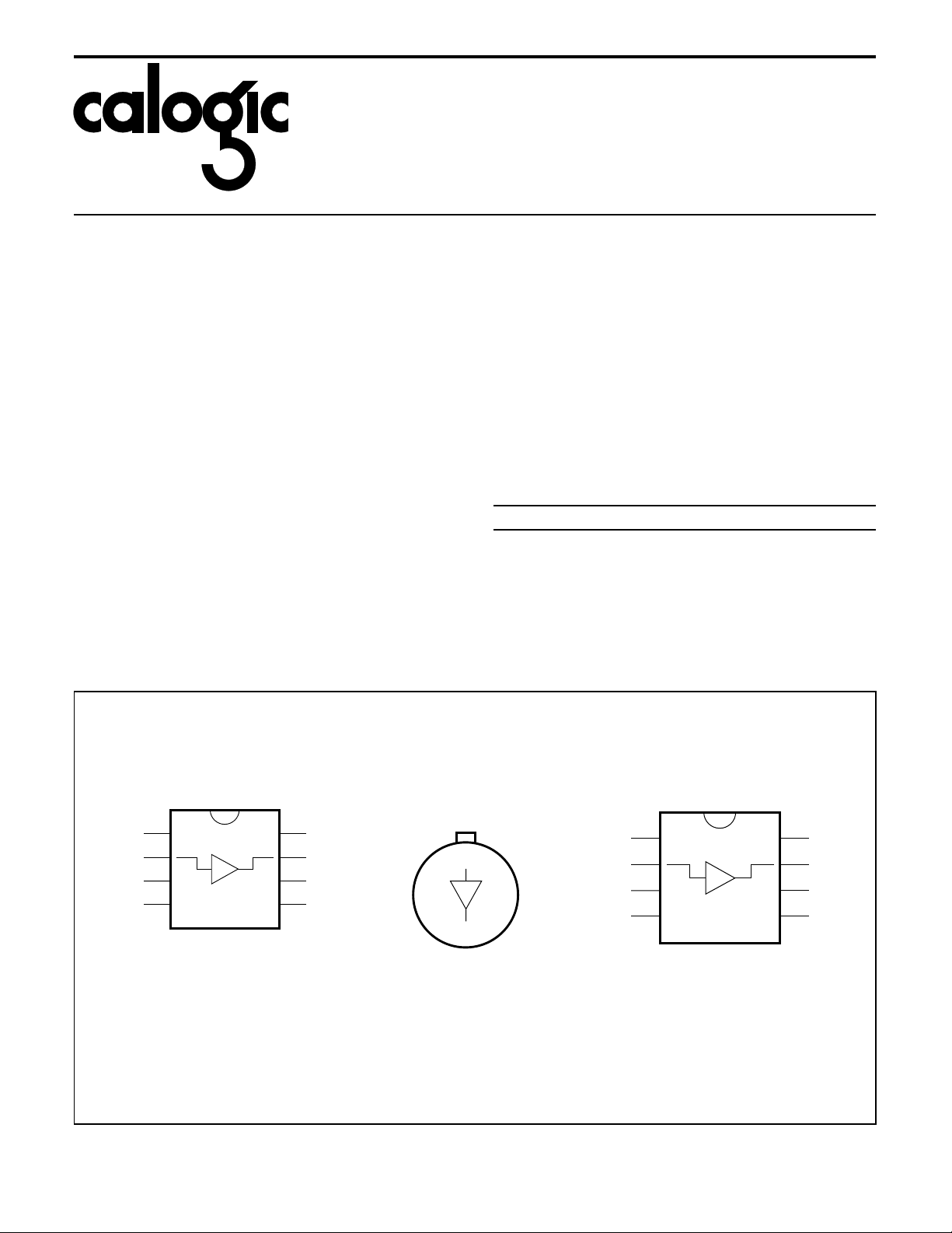
CONNECTION DIAGRAMS
GENERAL DESCRIPTION
The CLM6121 family are high speed unity gain buffers that slew
at 1200 V/ µs, having a small signal bandwidth of 100MHz, and
capable of providi ng a continuous output current of ±200mA.
They are monolithic ICs which are pin to pin compatible with
the LH0002H/CH with the additional feature of current limiting.
The internal output short circuit current limiting feature has
been designed in the device such that when the junction
temperat ur e reac hes 1 7 0
o
C, the current is limited to 100mA.
ORDERING INFORMATION
Part Package Temperature Range
o
CLM6121 H Hermetic TO5 8 Lead -55
CLM6321 H Hermetic TO5 8 Lead -40
CLM6121 N Plastic P Dip 8 Lead -40
CLM6321 N Plastic P Dip 8 Lead -40
CLM6121 M SOIC 8 Lead -25
CLM6321 M SOIC 8 Lead -25
C to 125oC
o
C to 85oC
o
C to 85oC
o
C to 85oC
o
C to 70oC
o
C to 70oC
Plastic DIP
1
*V-
2
V
IN
3
N/C
45
*V-
*Heat-sinking pins. Pin 1 and Pin 8
must be connected to the negative supply.
Package NO8A Package HO8A Package MO8A
8
V-*
7
V
OUT
6
V+
V-*
V
2+
V
1+
N/C
Metal Can
1
2
3
Top View
Plastic SO
V
IN
8
4
V
OUT
V
1-
7
6
V
2-
5
N/C
must be connected to the negative supply.
1
*V- V-*
2
V
IN OUT
3
N/C
45
*V- V-*
*Heat-sinking pins. Pin 1 and Pin 8
8
7
V
6
V+
CALOGIC CORPORATION, 237 Whitney P lac e, Fremont, California 94539, Telephone: 510- 65 6- 2 900, F AX: 510-651- 10 76
Page 2
CLM6121 / CLM6321
ABSOLUTE MAXIMUM RATINGS (Note 1)
If Military/Aerospace specified devices are required, please
contact the Calogic Sales Office for availability and
specifications.
Supply Voltage. . . . . . . . . . . . . . . . . . . . . . . . . . . . . . . . . . ±18
Input Voltage . . . . . . . . . . . . . . . . . . . . . . . . . . . . . . ±Vsupply
Short Circuit to GND (Not e 2) . . . . . . . . . . . . . . . . Continuous
Storage Temperatur e Ra nge. . . . . . . . . . . . -65
Lead Temperature
(Soldering 10 se conds) . . . . . . . . . . . . . . . . . . . . . . 260
DC ELECTRICAL CHARACTERISTICS
The following specifications apply for Supply Vo ltag e = ±15V, V
Boldface limits apply for T
= TJ = T
A
SYMBOL CHARACTERISTICS TYP
MIN
to T
o
C to +150oC
o
C
; all other limits TA = TJ = 25oC.
MAX
CLM6121 CLM6321
Limit
(Note 6)
CORPORATION
ESD Tolerance (Note 4). . . . . . . . . . . . . . . . . . . . . . . ±2000V
Therma l Re sistance (θ
) (Note 7)
JA
H Package . . . . . . . . . . . . . . . . . . . . . . . . . . . . . . 125
N Package . . . . . . . . . . . . . . . . . . . . . . . . . . . . . . . 50
M Package. . . . . . . . . . . . . . . . . . . . . . . . . . . . . . . 60
Therma l Re sistance (θ
JC
)
H Package . . . . . . . . . . . . . . . . . . . . . . . . . . . . . . . 15
= 0, RL ≥ 100kΩ and RS = 50Ω unless otherwise no ted.
CM
Limit
(Note 6)
UNITS CONDITIONS
o
C/W
o
C/W
o
C/W
o
C/W
A
V1
A
V2
A
V3
V
OS
I
B
R
IN
C
IN
R
O
I
S1
I
S2
V
O1
V
O2
Voltage Gain 1 0.990
Voltage Gain 2 0.900
Voltage Gain 3 0.840
Offset Voltage 15
Input Bias Current 1
Input Resistance 5 MΩ RL = 50Ω
Input Capacitance 3.5 pF
Output Resistance 3
Supply Current 1 15
Supply Current 2 14
Output Swing 1 13.5
Output Swing 2 12.7
0.980
0.970
0.860
0.800
0.780
0.750
30
50
4
7
5
10
18
20
16
18
13.3
13
11.5
10
0.970
0.950
0.850
0.820
0.750
0.700
50
100
5
7
5
6
20
22
18
20
13.2
13
11
10
V/V Min
mV Max R
µA Max R
Ω Max I
mA Max
±V Min
RL = 1kΩ, VIN = ±10V
R
= 50Ω, VIN = ±10V
L
R
= 50Ω, V+ = 5V
L
V
= 2V
IN
PP
= 1kΩ
L
= 1kΩ, RS = 10kΩ,
L
= ±10mA
OUT
R
= ∞
L
R
= ∞, V+ = 5V
L
R
= 1k
L
R
= 100Ω
L
V
O3
V
O4
PSSR
Output Swing 3 12
Output Swing 4 1.8
Power Supply
Rejection Ratio
70
11
9
1.6
1.3
60
55
10
1.6
1.5
60
50
R
= 50Ω
9
V
Min RL = 50Ω, V+ = 5V (Note 6)
PP
dB Min V
L
±
= ±5V to ±15V
CALOGIC CORPORATION, 237 Whitney P lac e, Fremont, California 94539, Telephone: 510 - 65 6- 2 900, F AX: 510-651- 10 76
Page 3

CORPORATION
CLM6121 / CLM6321
AC ELECTRICAL CHARACTERISTICS
The following specifications apply for Supply Vo ltag e = ±15V, V
Boldface limits apply for T
= TJ = T
A
SYMBOL CHARACTERISTICS TYP
SR
SR
SR
1
2
3
Slew Rate 1 1200 550 550 V/µsVIN = ±11V, RL = 1kΩ
Slew Rate 2 800 550 550 V/µsVIN = ±5V, RL = 50Ω (Note 3)
Slew Rate 3 650 550 550 V/µs
BW -3 dB Bandwidth 50 30 30 MHz
, t
t
r
f
t
pd
O
S
Rise Time
Fall Time
Propagation Delay Time 4.0 ns
Overshoot 10 %
Note 1: Absolute Maximu m Rating s indicate limits beyond which dama ge to the device may occur. DC and AC electrical specification s do no t
apply when operating the device beyond its rated operati ng conditi on s.
Note 2: The CLM6121 series buffers contain current limit and thermal shutdown to protect against fault conditions.
Note 3: Slew rate is measured with a ±11V input pulse and 50Ω source impedance at 25
should be at least 1700V/µs.
Note 4: The test circuit consists of the human body model of 120pF in series with 1500Ω.
Note 5: The maximum power dissipation is a function of T
temperature is P
D
= (T
J(max)
- TA)/θJA.
Note 6: Limits are guaranteed by testing, correlation or periodic characterization.
Note 7: For M & N package, θ
is measured by soldering the unit directly on a printed circuit board and V- pins are connected to 2 square
JA
inches of 2 oz copper.
MIN
to T
; all other limits TA = TJ = 25oC.
MAX
CLM6121 CLM6321
Limit (Note 6) Limit (Note 6)
7.0 ns
J(max), θJA
= 0, RL ≥ 100kΩ and RS = 50Ω unless otherwise no ted.
CM
UNITS CONDITIONS
V
= 2 VPP, RL = 50Ω
IN
+
V
= 5V
V
= ±100 mVPP, RL = 50Ω
IN
C
≤ 10pF
L
R
= 50Ω, CL ≤ 10pF
L
V
= 100mV
O
R
= 50Ω, CL ≤ 10pF
L
V
= 100mV
O
R
= 50Ω, CL ≤ 10pF
L
V
= 100mV
O
o
C. For accurate measurements, the input slew rate
PP
PP
PP
and TA. The maximum allowable power dissipation at any ambient
CALOGIC CORPORATION, 237 Whitney P lac e, Fremont, California 94539, Telephone: 510 - 65 6- 2 900, F AX: 510-651- 10 76
Page 4

CLM6121 / CLM6321
CORPORATION
PSSR
NEGATIVE
SUPPLY
vs Frequency
V
RIPPLE
R
S
FREQUENCY (Hz)
V = ±15V
= R
T
POSITIVE
SUPPLY
+80
+70
+60
+50
+40
+30
+20
+10
0
POWER SUPPLY REJECTION RATIO (dB)
100k 1M 10M 100M
Slew Rate
vs Temperature
= 1kR
L
= ±10V
V
IN
R
L
V
IN
V = ±15V
S
-25 25 75 125
JUNCTION TEMPERATURE (˚C)
s)
µ
SLEW RATE (V/
1250
1000
750
500
250
0
S
= 100mV
= 50Ω
L
= 25˚C
J
= 50Ω
= ±5V
Rise Time
10
8
6
4
RISE TIME (ns)
2
0
vs Temperature
V = ±5V
S
V = ±15V
S
= 50Ω
R
L
= 1kR
L
= 100mV
V
OUT
f = 1MHz
-25 25 75 125
TEMPERATURE (˚C)
Slew Rate
vs Capacitive Load
= 1kR
L
= ±10V
V
IN
= 50Ω
R
L
V
= ±5V
IN
0
10 40 100 400
CAPACITIVE LOAD (pF)
s)
µ
SLEW RATE (V/
1250
1000
750
500
250
pp
SR =
200mA
C
L
V = ±5V
S
V = ±15V
S
V = ±15V
S
T
= 25˚C
J
10002000
175
SLEW RATE (V/µs)
OUTPUT RESISTANCE (Ω)
1250
1000
750
500
250
0
50
40
30
20
10
0
Slew Rate
vs Supply Voltage
TJ= 25˚C
±5
SUPPLY VOLTAGE (±V)
Output Resistance
vs Supply Voltage
TJ= -55˚C
±5
SUPPLY VOLTAGE (±V)
±10 ±15 ±200
±10 ±15 ±200
R
I
OUT AC
I
OUT DC
T
= +125˚C
J
T
= +25˚C
J
= 50Ω
L
= 1kR
L
= 1mA
= 0
OUTPUT IMPEDANCE (Ω)
1000
100
10
1
Output Impedance
vs Frequency
V = ±15V
S
T
= 25˚C
J
= 100µA
I
OUT AC
R = 100k
S
1M
FREQUENCY (Hz)
Supply Current
20
18
16
14
12
10
8
6
4
= 50Ω
R
S
10M 100M100k
SUPPLY CURRENT (mA)
2
0
vs Supply Voltage
TJ= -55˚C
±5
SUPPLY VOLTAGE (V)
T
±10 ±15 ±200
= +25˚C
J
I
OUT
= +125˚C
T
J
= 0mA
+50
+40
+30
A)
µ
+20
+10
0
-10
-20
INPUT CURRENT (
-30
-40
-50
Input Current
vs Supply Voltage
T
= +125˚C
J
±5
SUPPLY VOLTAGE (V)
TJ= +25˚C
TJ= -55˚C
±10 ±15 ±200
= 0V
V
IN
CALOGIC CORPORATION, 237 Whitney P lac e, Fremont, California 94539, Telephone: 510 - 65 6- 2 900, F AX: 510-651- 10 76
Page 5

CORPORATION
CLM6121 / CLM6321
Input Resistance
100
40
)
Ω
20
10
4.0
2.0
1.0
0.4
INPUT RESISTANCE (M
0.2
0.1
vs Temperature
V = ±15V
S
= ±12V
V
IN
= 100Ω
R
L
-25 25 75 125
JUNCTION TEMPERATURE (˚C)
Voltage Gain vs Frequency
50Ω Resistive Load -
25
20
15
10
5
0
-5
-10
VOLTAGE GAIN (dB)
-15
-20
-25
Different Capacitive Loads
V = ±15V
S
= 50Ω
R
L
T
= 25˚C
J
VO< 100mV
= 0.01µF
C
L
C
= 1000pF
L
C
1 4 10 40 100 200
FREQUENCY (MHz)
= 500pF
L
C
L
= 100pF
VOLTAGE GAIN (dB)
175
PHASE SHIFT (DEGREES)
Voltage Gain vs Frequency
Different Resistive Loads -
25
20
15
10
Fixed Capacitive Load
V = ±15V
S
C
< 10pF
L
T
= 25˚C
J
VO= 100mV
R
L
R> 1k
L
= 100Ω
5
0
-5
-10
-15
-20
-25
1 4 10 40 100 200
= 50Ω
R
L
= 10Ω
R
L
FREQUENCY (MHz)
Phase Shift vs Frequency
Different Resistive Loads
= ∞
R
0
-10
-20
= 10Ω
R
-30
L
-40
-50
V = ±15V
-60
R
-70
T
-80
VO< 100mV
-90
1 4 10 40 100 200
S
= 50Ω
S
= 25˚C
J
R
L
= 50Ω
FREQUENCY (MHz)
L
Voltage Gain vs Frequency
No Resistive Load -
25
20
15
10
Different Capacitive Loads
= 0.01µF
C
L
C
= 500pF
L
CL= 100pF
CL= 1000pF
5
0
-5
V = ±15V
-10
S
VOLTAGE GAIN (dB)
= 10MΩ
R
L
-15
T
= 25˚C
J
-20
VO< 100mV
-25
1 4 10 40 100 200
FREQUENCY (MHz)
Phase Shift vs Frequency
0
-10
-20
-30
-40
-50
-60
-70
PHASE SHIFT (DEGREES)
-80
-90
100k 1M 10M 100M
Different Source Resisters
R= 1k
S
R = 10k
S
V = ±15V
S
= 50Ω
R
L
T
= 25˚C
J
VO< 100mV
FREQUENCY (Hz)
R
S
= 50Ω
Small Signal Bandwidth
vs Supply Voltage
= 100mV
V
IN
= 50Ω
R
L
= 50Ω
R
S
±5
SUPPLY VOLTAGE (±V)
TJ= -55˚C
= +25˚C
T
J
±10 ±15 ±200
= +125˚C
T
J
-3 dB BANDWIDTH (MHz)
200
150
100
50
0
CALOGIC CORPORATION, 237 Whitney P lac e, Fremont, California 94539, Telephone: 510 - 65 6- 2 900, F AX: 510-651- 10 76
 Loading...