

Datasheet CLM4426EP, CLM4426CY, CLM4426CP, CLM4428EY, CLM4428EP Datasheet (Calogic LLC)
...Page 1
CORPORATION
EFFECTIVE
INPUT
C = 12pF
300mV
OUTPUT
INPUT
GND
4.7V
V
DD
1L-11
INVERTING
OUTPUTS
2mA
NONINVERTING
OUTPUTS
CLM4426/CLM4427/CLM4428
1. CA4428 has one inverting and one noninvert i ng driver.
2. Ground any unused driver input.
NOTES:
1.5A Dual High Speed
MOSFET Drivers
CLM4426 / CLM4427 / CLM4428
FEATURES
•• High Peak Out put Curr ent . . . . . . . . . . . . . . . . . . . >1.5A
•• Fast Switching . . . . . . . . . . . . . . . . . . . . . . . . . . t
= 40ns
D
•• Wide Operating Range . . . . . . . . . . . . . . . . . 4.5V to 18V
•• Matched Rise and Fall Times
•• ESD Protected . . . . . . . . . . . . . . . . . . . . . . . . . . . . . . . 4kV
APPLICATIONS
•• Motor Cont ro ls
•• Switch Mode Power Supplies
•• Pulse Transformer Driver
•• Class D Sw i tc hing Amplifie rs
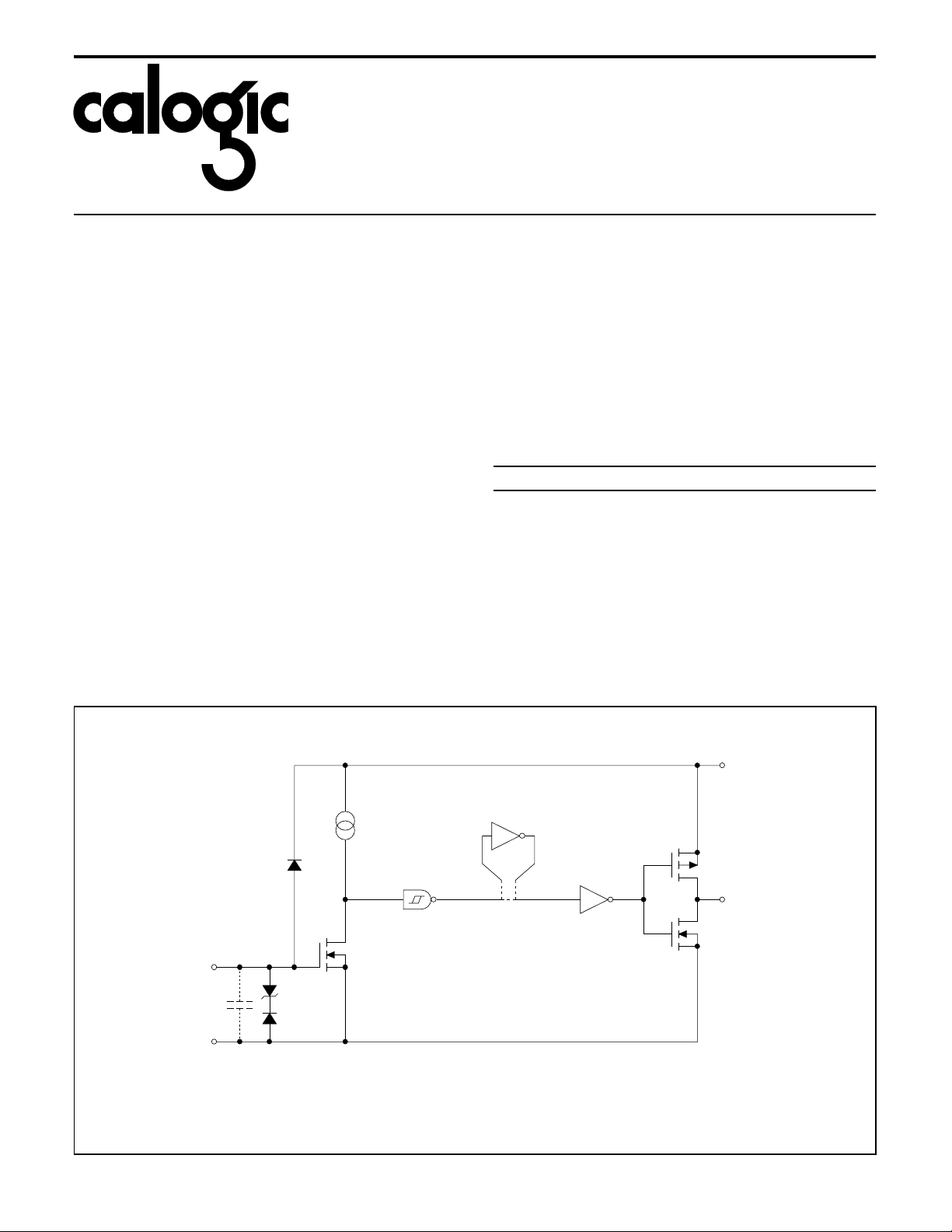
FUNCTIONAL DIAGRAM
DESCRIPTION
The CLM4426 series are dual CMOS drivers are designed to
drive capacitive, resistive and inductive loads switching
1000pF gate capacitances in under 30ns while providing low
impedances in both the ON and OFF states to insure the
MOSFET’s intended state will not be affected. All termi nals
are fully protect ed up to 4kV of ESD.
ORDERING INFORMATION
Part Logic Package Temperature
o
CLM4426CP Inverting 8 Pin PDIP 0
CLM4426EP Inverting 8 Pin PDIP -40
CLM4426CY Inverting 8 Pin SOIC 0
CLM4426EY Inverting 8 Pin SOIC -40
CLM4427CP Noninverting 8 Pin PDIP 0
CLM4427EP Noninverting 8 Pin PDIP -40
CLM4427CY Noninverting 8 Pin SOIC 0
CLM4427EY Noninverting 8 Pin SOIC -40
CLM4428CP Differential 8 Pin PDIP 0
CLM4428EP Differential 8 Pin PDIP -40
CLM4428CY Differential 8 Pin SOIC 0
CLM4428EY Differential 8 Pin SOIC -40
C to 70oC
o
C to 85oC
o
C to 70oC
o
C to 85oC
o
C to 70oC
o
C to 85oC
o
C to 70oC
o
C to 85oC
o
C to 70oC
o
C to 85oC
o
C to 70oC
o
C to 85oC
CALOG IC CO RP OR ATION, 237 Whitney Place, Fremont, California 94539, T elephone: 510-656-2900, FAX: 510-651-3025
Page 2
CLM4426 / CLM4427 / CLM4428
ABSOLUTE MAXIMUM RATINGS
Supply Voltage. . . . . . . . . . . . . . . . . . . . . . . . . . . . . . . . . +22V
Input Voltage, IN A or IN B. . . . . . . . . V
Maximum Ch ip Tem perature . . . . . . . . . . . . . . . . . . . . +150
Storage Tem per at ure Ra nge. . . . . . . . . . . . . -6 5
Lead Temperature (Soldering , 10 sec) . . . . . . . . . . . . +300
Package Ther mal Resist an ce
PDIP R
PDIP R
SOIC R
SOIC R
. . . . . . . . . . . . . . . . . . . . . . . . . . . . . . . 125oC/W
θJ-A
. . . . . . . . . . . . . . . . . . . . . . . . . . . . . . . . 42oC/W
θJ-C
. . . . . . . . . . . . . . . . . . . . . . . . . . . . . . . 250oC/W
θJ-A
. . . . . . . . . . . . . . . . . . . . . . . . . . . . . . . . 75oC/W
θJ-C
Operating Temperatur e Ra nge
C Version. . . . . . . . . . . . . . . . . . . . . . . . . . . . 0
E Version . . . . . . . . . . . . . . . . . . . . . . . . . . . -40
Power Dissipation
Plastic. . . . . . . . . . . . . . . . . . . . . . . . . . . . . . . . . . . 1000mW
SOIC . . . . . . . . . . . . . . . . . . . . . . . . . . . . . . . . . . . . 500mW
Static-sensitive device. Unused devices must be stored in conductive
material. Protect devices from static discharge and static fields.
Stresses above t hose listed under "Ab solute Maximum Ratings" m ay
cause permanent damage to the device. These are stress ratings
only and functional operation of the device at these or any other
conditions above those indicated in the operation sections of the
specifications is not implie d. Exposure to absolute maximum rating
conditions for extended periods ma y aff ect device reliability.
+0.3V to GND-5.0V
DD
o
C to +150oC
o
C to +70oC
o
C to +85oC
o
o
CORPORATION
C
C
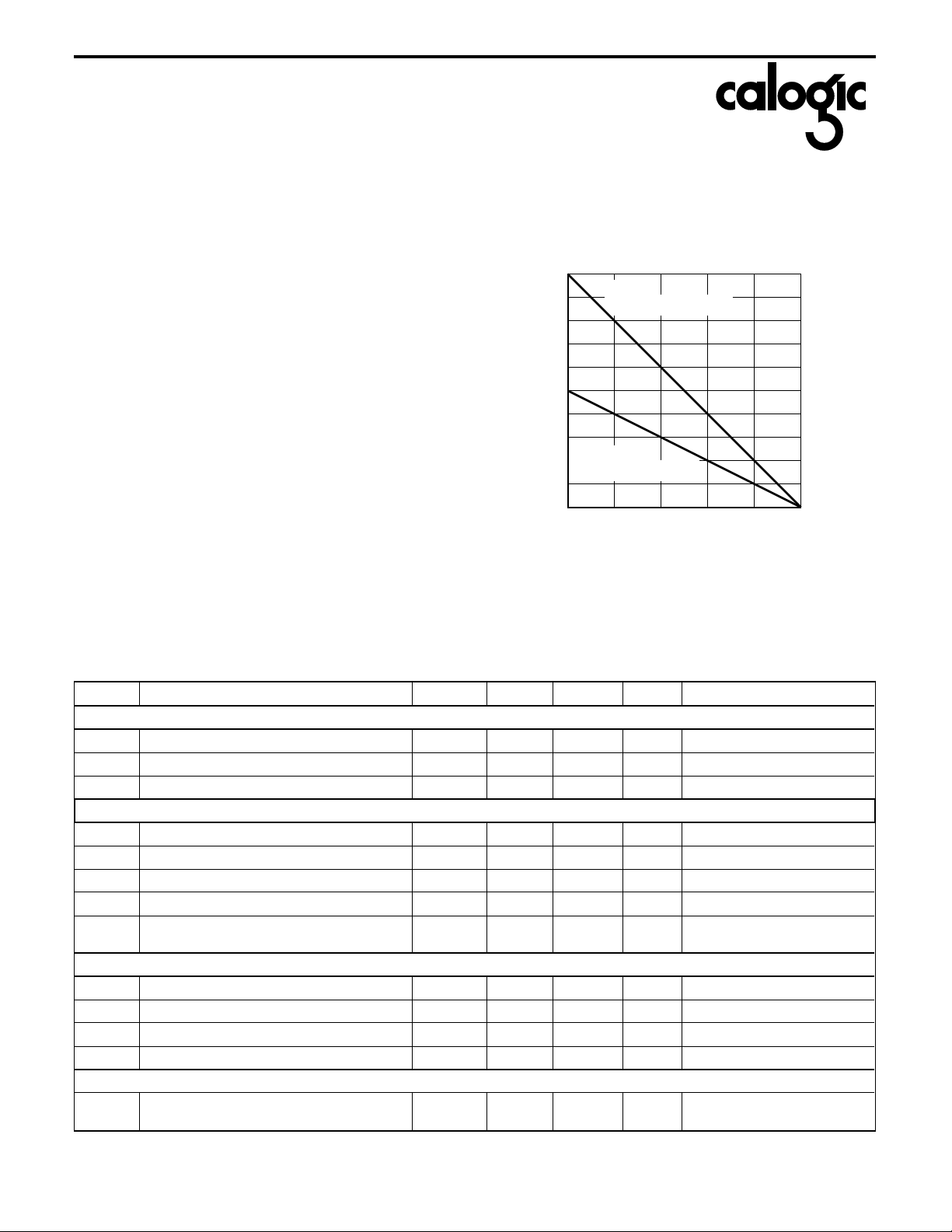
1000
PACKAGE POWER
DISSIPATION
PDIP
SLOPE = –8mW/˚C
800
600
(mW)P
D
400
SOIC
200
SLOPE = –4mW/˚C
0
25 150
AMBIENT TEMPERATURE (˚C)
1251007550
1B-38
ELECTRICAL CHARACTERISTIC S T
SYMBOL PARAMETER MIN TYP MAX UNIT TEST CONDITIONS
INPUT
V
IH
V
IL
I
IN
OUTPUT
V
OH
V
OL
R
O
I
PK
I
REV
SWITCHING TIME (Note 1)
t
R
t
F
t
D1
t
D2
POWER SUPPLY
I
S
Note: 1. Switching times are guaranteed by design.
Logic 1 High Input Voltage 2.4 - - V
Logic 0 Low Input Voltage - - 0.8 V
Input Current -1 - 1 µA 0V ≤ VIN ≤ V
High Output Voltage VDD-0.025 - - V
Low Output Voltage - - 0.025 V
Output Resistance - 7 10 Ω VDD = 18V, IO = 10mA
Peak Output Current - 1.5 - A
Latch-Up Protection
Withstand Reverse Current
Rise Time - 25 30 ns Figure 1
Fall Time - 25 30 ns Figure 1
Delay Time - - 30 ns Figure 1
Delay Time - - 50 ns Figure 1
Power Supply Current -
= +25oC with 4.5V ≤ VDD ≤ 18V , unles s ot herwise spe cified.
A
>0.5 - - A Duty Cycle ≤ 2%
-
-
-
4.5
0.4
mAmAVIN = 3V (Both Inputs)
DD
t ≤ 300µs
V
= 0V (Both Inputs)
IN
CALOG IC CORPORATION, 237 Whitney Place, Fremont, California 94539, Telephone: 510-656-2900, FAX: 510-651-3025
Page 3

CORPORATION
!L-12
NC 1
2
3
8
7
6
4
5
IN A
GND
IN B
OUT A
NC
V
DD
OUT B
NC 1
2
3
8
7
6
4
5
IN A
GND
IN B
OUT A
NC
V
DD
OUT B
NC
1
2
3
8
7
6
45
IN A
GND
IN B
OUT A
NC
V
DD
OUT B
2,4 7,5
INVERTING
NC = NO INTERNAL CONNECTION
2,4 7,5
NONINVERTING
NOTE: SOIC pinout is identical to DIP.
27
45
DIFFERENTIAL
CLM4426 CLM4427 CLM4428
PIN CONFIGU R ATIONS
CLM4426 / CLM4427 / CLM4428
ELECTRICAL CHARACTERISTIC S
Specifications measur ed over te mper at ure ra nge with 4. 5V ≤ V
SYMBOL PARAMETER MIN TYP MAX UNIT TEST CONDITIONS
INPUT
V
IH
V
IL
I
IN
OUTPUT
V
OH
V
OL
R
O
I
PK
I
REV
SWITCHING TIME (Note 1)
t
R
t
F
t
D1
t
D2
POWER SUPPLY
I
S
Note: 1. Switching times are guaranteed by design.
Logic 1 High Input Voltage 2.4 - - V
Logic 0 Low Input Voltage - - 0.8 V
Input Current -1 - 1 µA 0V ≤ VIN ≤ V
High Output Voltage VDD-0.025 - - V
Low Output Voltage - - 0.025 V
Output Resistance - 9 12 Ω VDD = 18V, IO = 10mA
Peak Output Current - 1.5 - A
Latch-Up Protection
Withstand Reverse Current
Rise Time - - 40 ns Figure 1
Fall Time - - 40 ns Figure 1
Delay Time - - 40 ns Figure 1
Delay Time - - 60 ns Figure 1
Power Supply Current -
>0.5 - - A Duty Cycle ≤ 2%
≤ 18V, unless othe rwise specified.
DD
-
-
-
8
0.6
DD
t ≤ 300µs
mAmAVIN = 3V (Both Inputs)
V
= 0V (Both Inputs)
IN
CALOG IC CORPORATION, 237 Whitney Place, Fremont, California 94539, Telephone: 510-656-2900, FAX: 510-651-3025
Page 4

CLM4426 / CLM4427 / CLM4428
FIGURE 1. SWITCHING TIME TEST CIRCUI T
CORPORATION
INPUT
+5V
INPUT
10%
= 18V
V
DD
0.1
4.7
µF
6
2,4
5,7
3
µF
C
= 1000pF
L
OUTPUT
≈0.4V
V
OUTPUT
+5V
INPUT
≈0.4V
V
OUTPUT
DD
0V
10%
DD
0V
90%
t
t
F
D1
10%
INVERTING DRIVER
90%
t
D1
t
NONINVERTING DRIVER
90%
t
D2
t
R
90%
10%
90%
R
t
90%
D2
10%10%
1B-40
t
F
10
–8
9
8
7
6
CROSSOVER ENERGY LOSS
5
4
sec
3
•
A
2
–9
10
418
V
DD
NOTE:
The values on this graph represent the loss seen by both
1614121086
drivers in a package during one complete cycle. For a single
driver, divide the stated values by 2. For a single transition of a
single driver, divide the stated value by 4.
1B-41
CALOG IC CORPORATION, 237 Whitney Place, Fremont, California 94539, Telephone: 510-656-2900, FAX: 510-651-3025
 Loading...