

Page 1
CORPORATION
High Speed Buffer
CLM4121 / CLM4321
FEATURES
High Slew Rat e. . . . . . . . . . . . . . . . . . . . . . . . . . 2000V/µs
••
Wide Ban dw idt h. . . . . . . . . . . . . . . . . . . . . . . . . . 180MHz
••
Peak Output Current. . . . . . . . . . . . . . . . . . . . . . . 300m A
••
Low Supply Current . . . . . . . . . . . . . . . . . . . . . . . . . 7mA
••
No Oscillations w it h Capacitive Lo ads
••
5V to ±15V O per ation Gua r anteed
••
Fully S p e ci fi e d to Drive 50Ω Lines
••
APPLICATIONS
Coaxial Ca ble Driv er
••
Flash A/D Converter Driver
••
Video DAC Buffer
••
OP Amp Booster
••
Video Am pl ifier
••
High Frequency Filter
••
Wide Ban dwi dt h Signal Condi t ioni ng
••
Radar
••
Sonar
••
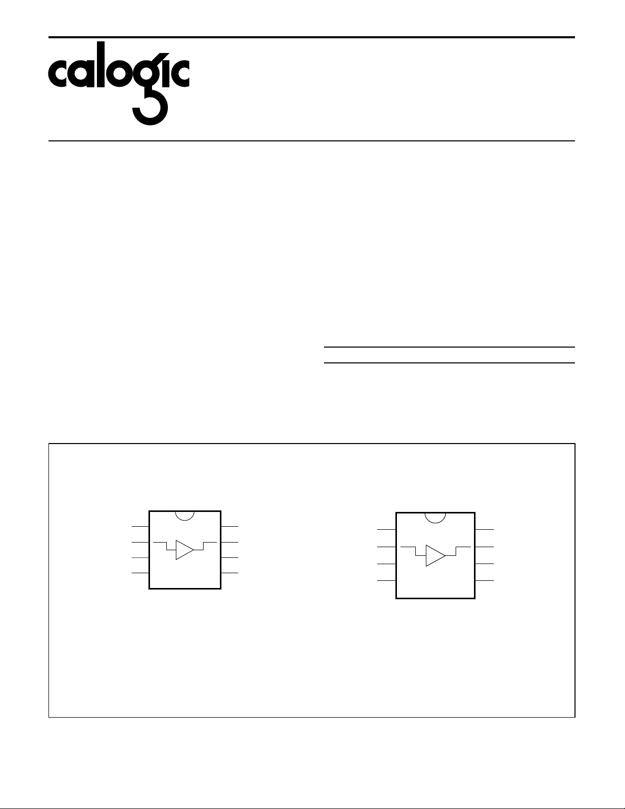
CONNECTION DIAGRAMS
Plastic DIP
GENERAL DESCRIPTION
The CLM4121 family are high speed unity gain buffers that
slew at 2000V/µs, having a small signal bandwidth of
180MHz, del ivers 150m A, yet dr aws on ly 7mA supply curren t.
The fast slew rate, wide bandwidth, and high output drive
make the CLM4121 family the ideal choice for closed loop
buffer appl ications with wide band op amps.
These same characteristics are the excellent choices for ope n
loop applications such as driving coaxial and switched pair
cables.
ORDERING INFORMATION
Part Package Temperature Range
o
CLM4121 N NO8A (Plas tic P Dip 8 Lead) -40
CLM41 21 M MO8B (SO I C 8 Le a d) -40
CLM4321 N NO8A (Plas tic P Dip 8 Lead) -25
CLM43 21 M MO8B (SO I C 8 Le a d) -25
Plastic SO
C to 85oC
o
C to 85oC
o
C to 70oC
o
C to 70oC
1
*V-
2
V
IN
3
N/C
45
*V-
*Heat-sinking pins. Pin 1 and Pin 8
must be connected to the negative supply.
Package NO8A Package MO8B
CALOGIC CORPORATION, 237 Whitney P lac e, Fremont, California 94 53 9, Telephone: 510-656-2 90 0, FAX: 510-651- 10 76
8
V-*
7
V
OUT
6
V+
V-*
must be connected to the negative supply.
1
*V- V-*
2
V
IN OUT
3
N/C
45
*V- V-*
*Heat-sinking pins. Pin 1 and Pin 8
8
7
V
6
V+
Page 2
CLM4121 / CLM4321
ABSOLUTE MAXIMUM RATINGS (Note 1)
Supply Voltage. . . . . . . . . . . . . . . . . . . . . . . . . . . . . . . . . . ±20
Input Voltage . . . . . . . . . . . . . . . . . . . . . . . . . . . . . . ±Vsupply
Storage Temperature Ra nge. . . . . . . . . . . . -65
Lead Temper at ure
(Soldering 10 seconds) . . . . . . . . . . . . . . . . . . . . . . 260
Power Dissipation . . . . . . . . . . . . . . . . . . . . . . . . . . . (Note 4)
DC ELECTRICAL CHARACTERISTICS
The following specifications apply for Supply Vo ltag e = ±15V, V
Boldface limits apply for T
= TJ = T
A
SYMBOL CHARACTERISTICS TYP
MIN
to T
o
C to +150oC
o
C
; all other limits TA = TJ = 25oC.
MAX
CLM4121 CLM4321
Limit
(Note 5)
CORPORATION
ESD Tolerance (Not e 3). . . . . . . . . . . . . . . . . . . . . . . ±2000V
Therma l Re sistance (θ
) (Note 6)
JA
N Package . . . . . . . . . . . . . . . . . . . . . . . . . . . . . . . 50
M Package . . . . . . . . . . . . . . . . . . . . . . . . . . . . . . . 60
Maximum J unction Temperature . . . . . . . . . . . . . . . . . . 150
= 0, RL ≥ 100KΩ and RS = 50Ω unless otherwise noted.
CM
Limit
(Note 5)
UNITS CONDITIONS
o
C/W
o
C/W
o
C
A
V1
A
V2
A
V3
V
OS
I
B
R
IN
C
IN
R
O
I
S1
I
S2
V
O1
V
O2
Voltage Gain 1 0.970
Voltage Gain 2 0.900
Voltage Gain 3 0.840
Offset Voltage 15
Input Bias Current 1
Input Resistance 0.5 .2 .2 MΩ RL = 50Ω
Input Capacitance 3.5 pF
Output Resistance 3
Supply Current 1 7.5
Supply Current 2 2.5
Output Swing 1 13.5
Output Swing 2 12.7
0.950
0.950
0.800
0.800
0.780
0.750
20
30
5
7
5
10
10
10
5
5
13.3
13
10
9
0.950
0.950
0.800
0.800
0.750
0.700
30
30
10
10
5
6
10
10
5
5
13.2
13
10
9
V/V Min
mV Max R
µA Max R
Ω Max I
mA Max
±V Min
RL = 1KΩ, VIN = ±10V
R
= 50Ω, VIN = ±6V
L
R
= 50Ω, V+ = 5V
L
V
= 2V
IN
PP
= 1KΩ
L
= 1KΩ, RS = 10kΩ,
L
= ±10mA
OUT
RL = ∞
R
= ∞, V+ = 5V
L
R
= 1K
L
R
= 100Ω
L
V
O3
I
OUT
PSSR
Output Swing 3 1.8
1.6
1.3
Output Current 200 140 140 mA VIN = ±13V
Power Supply
Rejection Ratio
70
60
60
1.6
1.5
60
60
V
Min RL = 50Ω, V+ = 5V (Note 5)
PP
dB Min V
±
= ±5V to ±15V
CALOGIC CORPORATION, 237 Whitney P lac e, Fremont, California 94 53 9, Telephone: 510-656-2 90 0, FAX: 510-651- 10 76
Page 3

CORPORATION
AC ELECTRICAL CHARACTERISTICS
The following specifications apply for Supply Vo ltag e = ±15V, V
Boldface limits apply for T
= TJ = T
A
MIN
to T
; all other limits TA = TJ = 25oC.
MAX
CLM4121 / CLM4321
= 0, RL ≥ 100KΩ and RS = 50Ω unless otherwise noted.
CM
SYMBOL CHARACTERISTICS TYP
CLM4121 CLM4321
UNITS CONDITIONS
Limit (Note 5) Limit (Note 5)
SR
SR
SS
LS
P
t
r
t
pd
O
BW
, t
S
1
2
BW
BW
f
Slew Rate 1 4000 3500 2500
V/µs
VIN = ±11V, RL = 1KΩ (Note 2)
Slew Rate 2 2000 1500 1000 VIN = ±5V, RL = 50Ω (Note 2)
V
= ±100mVPP, RL = 50Ω
Small Signal Bandwidth 180 140 100
Large Signal Bandwidth 65 55 40
MHz
Power Bandwidth 40 30 20
Rise Time
Fall Time
2.0 2.5 3.5 ns
Propagation Delay Time 3.0 ns
Overshoot 10 %
IN
C
≤ 10pF
L
V
= ±11V, RL = 1K
IN
C
≤ 10pF
L
V
= ±8V, RL = 50Ω
IN
C
≤ 10pF
L
R
= 50Ω, CL ≤ 10pF
L
V
= 100mV
O
R
= 50Ω, CL ≤ 10pF
L
V
= 100mV
O
R
= 50Ω, CL ≤ 10pF
L
V
= 100mV
O
PP
PP
PP
Note 1: Absolute Maximu m Rating s indicate limits beyond which dama ge to the device may occur. DC and AC electrical specification s do no t
apply when operating the device beyond its rated operati ng conditi on s.
o
Note 2: Slew rate is measured with 50Ω source imped an ce at 25
C. For accurate measurements, the input slew rate should be at least
5000V/µs.
Note 3: The test circuit consists of the human body model of 120pF in series with 1500Ω.
Note 4: The maximum power dissipation is a function of T
temperature is P
D
= (T
J(max)
- TA)/θJA.
J(max), θJA
and TA. The maximum allowable power dissipation at any ambient
Note 5: Limits are guaranteed by testing, correlation or periodic characterization.
Note 6: For M & N package, θ
is measured by soldering the unit directly on a printed circuit board and V- pins are connected to 2 square
JA
inches of 2 oz copper.
CALOGIC CORPORATION, 237 Whitney P lac e, Fremont, California 94 53 9, Telephone: 510-656-2 90 0, FAX: 510-651- 10 76
Page 4

CLM4121 / CLM4321
TYPICAL PERFORMANCE CHARACTERI STI CS
CORPORATION
GAIN (dB)
30
24
18
P-P
(V )
IN
12
V
0
-2
-4
-6
-8
6
0
FREQUENCY RESPONSE
RL= 1K
V
≤ 100mV
IN
C
≤ 10pF
L
T
= 25˚C
j
11025
20 50 400100 200
FREQUENCY (MHz)
BANDWIDTH
(LARGE SIGNAL & POWER)
R
L
RL= 50Ω
11025
20 50 400100 200
FREQUENCY (MHz)
= 10K
80
64
48
32
16
0
FREQUENCY RESPONSE
PHASE LAG (DEGREES)
GAIN (dB)
0
-2
-4
-6
-8
RL= 50Ω
V
≤ 100mV
IN
C
≤ 10pF
L
T
= 25˚C
j
11025
FREQUENCY (MHz)
20 50 400100 200
80
60
40
20
0
PHASE LAG (DEGREES)
SUPPLY VOLTAGE
vs BANDWIDTH
RL= 1K
RL= 50Ω
2
4 6 8 10 12 14 16 18 20
SUPPLY VOLTAGE (±V)
-3dB BANDWIDTH (MHz)
300
280
260
240
220
200
180
160
140
120
100
80
60
40
20
0
SUPPLY VOLTAGE
vs SUPPLY CURRENT
11
10
9
8
7
6
5
4
SUPPLY CURRENT (±mA)
3
2
1
0
1
357911131517
SUPPLY VOLTAGE (±V)
19
s)
µ
SLEW RATE (V/
4500
4000
3500
3000
2500
2000
1500
1000
500
0.0
INPUT VOLTAGE
vs SLEW RATE
= 1K
R
L
RL= 50Ω
2 6 10 14 18 22
VIN(V )
P-P
CALOGIC CORPORATION, 237 Whitney P lac e, Fremont, California 94 53 9, Telephone: 510-656-2 90 0, FAX: 510-651- 10 76
Page 5

CORPORATION
MO8B DIMENSION S
12
.050
(1.27)
5678
34
.020
.013
.213
.205
(5.4)
(5.2)
(TOP VIEW)
MO8B-8 LEAD SOIC
(.50)
(.33)
.210
.205
(5.32)
(5.19)
.010
.004
.074
.070
(1.87)
(1.77)
(.25)
(.10)
.318
.302
(8.10)
(7.64)
.023
.019
.010
.006
(.25)
(.15)
(.58)
(.48)
CALOGIC CORPORATION, 237 Whitney P lac e, Fremont, California 94 53 9, Telephone: 510-656-2 90 0, FAX: 510-651- 10 76
Page 6

CORPORATION
NO8A DIMENSIONS
0.405 MAX
0.150
(3.81)
MIN
0.023
0.014
0.005
(1.13)
MAX
(0.58)
(0.36)
(10.29)
0.06
0.15
(1.52)
(0.38)
0.070
0.030
8-Pin Plastic Dip
0.055
(1.40)
MAX
0.200
(5.08)
MAX
0.200
(5.08)
0.125
(3.18)
(1.78)
(0.76)
0.320
(8.13)
0.290
(7.37)
0.310
(7.87)
0.220
(5.59)
0.015
o
15 MAX
All Dimensions in
inches and
0.290
(millimeters)
(0.38)
(0.20)
CALOGIC CORPORATION, 237 Whitney P lac e, Fremont, California 94 53 9, Telephone: 510-656-2 90 0, FAX: 510-651- 10 76
 Loading...