

Datasheet CLM2815AT-3.3, CLM2815AT-2.5, CLM2815AT-1.5, CLM2815AT, CLM2815AAU-5 Datasheet (Calogic LLC)
...Page 1
1.5A Low Dropout Voltage Regulator
Adjustable & Fixed Output
Fast Response
CLM2815
FEATURES
•• Adjustable Output . . . . . . . . . . . . . . . . . . . Down To 1.2V
•• Fixed Output Voltages. . . . . . . . . . . . . . 1.5, 2.5, 3.3, 5.0V
•• Output Current. . . . . . . . . . . . . . . . . . . . . . . . . . . . . . 1.5A
•• Low Dropout Voltage. . . . . . . . . . . . . . . . . . . . . 1.1V Ty p.
•• Extremely T ig ht Load And Line Regulation
•• Current & Thermal Limiting
•• Standard 3-Te rm i nal Low Cost T O -2 20, TO - 2 6 3 &
TO-252
•• Similar To Industr y Sta ndard LT10 86/ LT15 86
APPLICATIONS
•• Powering VGA & Soun d Card
•• Power PC Supplies
•• SMPS Post-Regula tor
•• High Effic ie ncy "Gr een " Co m put er System s
•• High Efficie ncy Line ar Powe r Supp lies
•• Portable I nst ru me nt atio n
•• Constant Curr ent Regulators
•• Adjusta ble Power Supplies
•• Battery charger
PRODUCT DESCRIPTION
Calogic’s CLM2815 is a low power 1.5A adjustable and fixed
voltage regulator. The device requires 2 external resistors to
set the output for the adjustable version. The CLM2815 has
been designed for low voltage applications that require lower
dropout and faster transient responses. The device is well
suited to power a low voltage microprocessor that requires a
low dropout and a fast transient response to regulate from
+2.85V to 3.8V. The device is adjustable t o 1.2 volts.
The product family offers full protection against over-current
faults, reversed input polarity, reversed load insertion, and
positive and negative transient voltage. On-chip trimming
adjusts the reference voltage to 1% while delivering 1.5A
output current.
Encapsulated in a 3-pin TO-22 0, TO-26 3 & T O-252 pa ckag es.
ORDERING INFORMATION
Part Package Temperature Range
CLM2815AU TO-220 -45 to +125
o
C
CLM2815AAU TO-220 -45 to +125
o
C
CLM2815AU-X TO-220 -45 to +125
o
C
CLM2815AAU-X TO-220 -45 to +125
o
C
CLM2815AT TO-263 (DD) -45 to +125
o
C
CLM2815AAT TO-263 (DD) -45 to +125
o
C
CLM2815AT - X TO-263 (DD) -45 to +125
o
C
CLM2815AAT -X TO-263 (DD) -45 to +125
o
C
CORPORATION
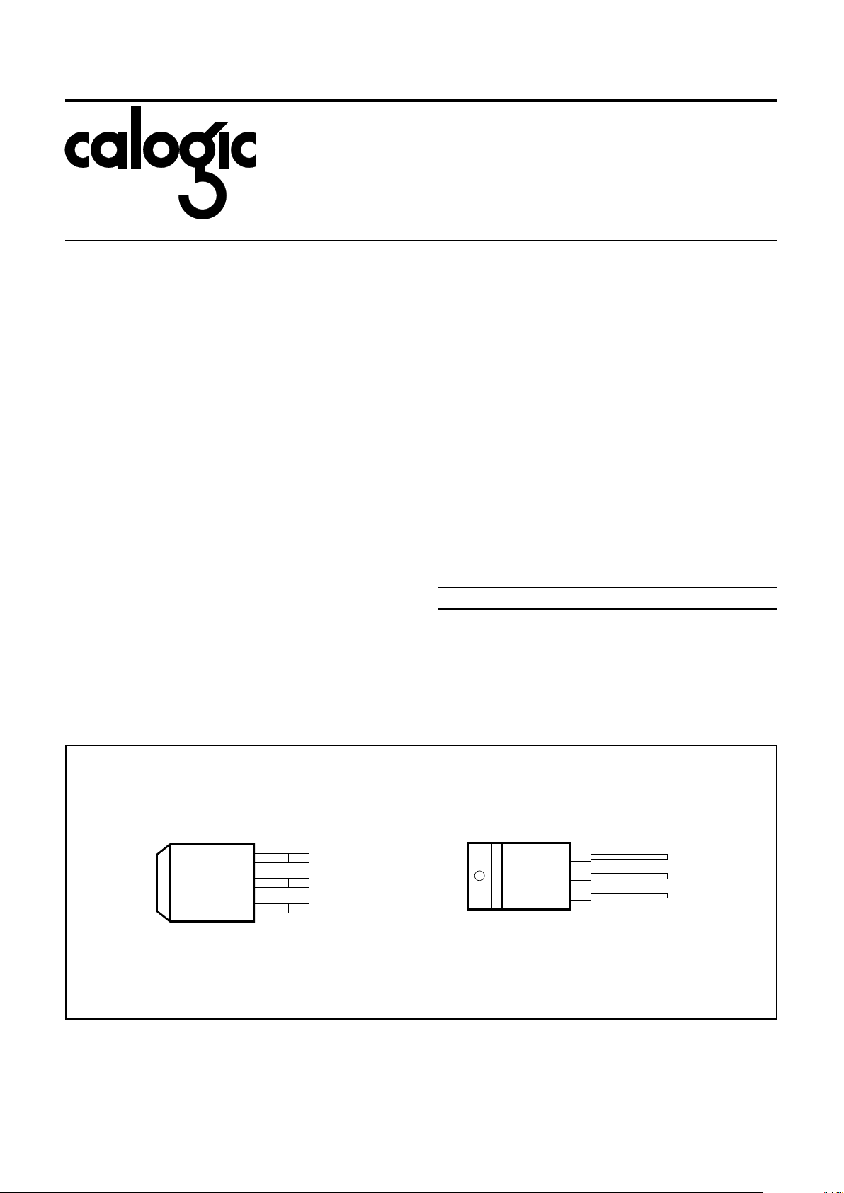
PIN CONNECTIONS
1E-30A
FRONT VIEW
V
IN
V
OUT
CLM2815
PLASTI C T O - 220 P A CK AG E
V
ADJ/GND
1E-29A
PLASTI C T O - 263 P A CK AGE
FRONT VIEW
CLM2815
3
2
1V
ADJ/GND
V
OUT
V
IN
CALOGIC CORPORATION, 237 Whitney Place, Fremont, California 94539, Telephone: 510 -656-290 0, FAX: 510-651-3025
Page 2
ABSOLUTE MAXIMUM RATINGS
Lead Temp. (Solder ing, 10 Se cond s) . . . . . . . . . . . . . . 300
o
C
Storage Te m per atur e Range . . . . . . . . . . . . -65
o
C to +150oC
Operating Junct ion Temperat ure Ran ge
CLM2815 Control Sectio n . . . . . . . . . . . . . . -45
o
C +125oC
CLM2815 Power Tr ans isto r . . . . . . . . . . . . . . -45
o
C +150oC
Input Voltage . . . . . . . . . . . . . . . . . . . . . . . . . . . . . . . . . . . 10V
Input to Output Voltage Differentia l . . . . . . . . . . . . . . . . . . 10V
Maximum Out pu t Current . . . . . . . . . . . . . . . . . . . . . . . . . . 2A
CALOGIC CORPORATION, 237 Whitney Place, Fremont, California 94539, Telephone: 510 -656-290 0, FAX: 510-651-3025
ELECTRICAL CHARACTERISTIC S (Note 1) at I
OUT
= 10mA, TA = 25oC, unless otherwise specified .
PARAMETER TYP
CLM2815A CLM2815
UNITS CONDITIONS
MIN MAX MIN MAX
1.5V VERSION
Output Voltage (Note 2)
1.5
1.5
1.485
1.470
1.515
1.530
1.470
1.455
1.530
1.545
V CLM2815-1.5V , 0 ≤ I
OUT
≤ 1.5A, 2.75V ≤ VIN ≤ 7V
2.5V VERSION
Output Voltage (Note 2)
2.5
2.5
2.475
2.450
2.525
2.550
2.450
2.425
2.550
2.575
V CLM2815-2.5V , 0 ≤ I
OUT
≤ 1.5A, 3.5V ≤ VIN ≤ 7V
3.3V VERSION
Output Voltage (Note 2)
3.3
3.3
3.270
3.240
3.330
3.360
3.230
3.201
3.370
3.399
V CLM2815-3.3V , 0 ≤ I
OUT
≤ 1.5A, 4.75V ≤ VIN ≤ 7V
5.0V VERSION
Output Voltage (Note 2)
5.0
5.0
4.95
4.90
5.05
5.10
4.900
4.850
5.100
5.150
V CLM2815-5.0V , 0 ≤ I
OUT
≤ 1.5A, 5.5V ≤ VIN ≤ 7V
ALL VOLTAGE OPTIONS
Reference Voltage
(V
REF
)
1.250 1.225 1.270 1.225 1.270 V
V
IN
≤ 7V, P ≤ P
MAX
1.5V ≤ (VIN - V
OUT
) ≤ 5.75V, 10mA ≤ I
OUT
≤ I
OUT
≤ 5.75
Min. Load Current (Note 3) 51010mA 1.5V ≤ (V
IN
- V
OUT
) ≤ 5.75V
Line Regulation
(∆V
REF
(IIN))
0.005 0.2 0.2
%
2.75V ≤ V
IN
≤ 7V, I
OUT
= 10mA, TJ = 125oC (Note 3)
0.005 0.2 0.2 V
IN
≤ 7V, I
OUT
= 0mA, TJ = 125oC (Note 2)
Load Regulation
(∆V
REF
(I
OUT
))
0.05 0.3 0.3
%
10mA ≤ I
OUT
≤ 1.5A, (VIN - V
OUT
) = 3V, TJ = 25oC
0.05 0.3 0.3 0 ≤ I
OUT
≤ 1.5A, VIN = 7V, TJ = 125oC (Note 2)
Dropout Voltage 1.1 1.2 1.2 V ∆V
REF
= 1%, I
OUT
= 1.5A (Note 3), I
OUT
≤ 1.5A (Note 2)
Current Limit
(I
OUT(MAX)
)
2.5 1.7 1.7 A
V
IN
= 7V ≤ 1.5A
1.4V ≤ (V
IN
- V
OUT
) (Note 3)
Long Term Stability
0.3
(Note 2)
11%T
A
= 125oC, 1000 Hrs.
Thermal Regulation
(∆V
OUT
(PWR))
0.01 0.020 0.020 %/W T
A
= 25oC, 20ms pulse
T emperature Stability
(∆V
OUT
(T))
0.25 %
Output Noise, RMS 0.003 %V
O
10Hz to 10kHz, TA = 25oC
Thermal Resistance
3.0
60
3.0
60
3.0
60
3.0
60
3.0
60
3.0
60
o
C/W
TO-220 Junction to Tab
Junction to Ambient
DD Package Junction to Tab
Junction to Ambient
The Bold specifications apply to the over full opera ting tem p era ture rang e.
Note 1: Changes in output voltage due to heating effects are covered under the specification for thermal regulation.
Note 2: Fixed version only.
Note 3: Adustable version only.
CLM2815
CORPORATION
Page 3

APPLICATION HINTS
The Calogic Semiconductor CLM2815 incorporates protect ion
against over-current faults, reversed load insertion, over
temperature operation, and positive and negative transient
voltage. However, the use of an output capacitor i s required
in order to insure the stability and the performances.
Stabilit y
The output capacitor is part of the regulator’s frequency
compensation system. Either a 220µF aluminum electrolytic
capacitor or a 47µF solid tantalum capacitor between the
output terminal and ground guarantees sta ble operat ion f or all
operating conditions.
However, in order to minimize overshoot and undershoot, and
therefore optimize the design, please refer to the section
’Ripple Rejection’.
Ripple Reject i on
Ripple rejection can be improved by adding a capacitor
between the ADJ pin and ground. When ADJ pin bypas sing is
used, the value of the output capacitor required increases to
its maximum (220µF for an aluminum electrolytic capacitor, or
47µF for a soli d tantalum capacitor). If the ADJ pin is not
bypass, the value of the output capacitor can be lowered to
100µF for an electrolytic aluminum capacitor or 15µF for a
solid tantalum capacit or.
However the value of the ADJ-bypass capacitor should be
chosen with respec t to the f ollo wing equa tion :
C = 1 / ( 6.28
•
FR • R1 )
Where C = value of the capacitor in Fara d s (select an equal or
larger standa rd value) ,
F
R
= ripple frequency in Hz,
R
1
= value of resistor R1 in Ohms.
If an ADJ-bypass capacitor is used, the amplitude of the
output ripple will be independent of the output voltage. If an
ADJ-bypass capacitor is not used, the output ripple will be
proportional to the ratio of the output voltage to the reference
voltage:
M = V
OUT
/ V
REF
Where M = multiplier for the ripple seen when the ADJ pin is
optimally bypassed .
V
REF
= Reference Voltage
Reducing parasit ic resis tance an d induct an ce
One solution to minimize parasitic resistance and inductance
is to connect in parallel capacitors. This arrangement will
improve the transient response of the power supply if your
system require s rapidly chan ging curr ent load condit io n.
Thermal Consideratio n
Although the CLM2815 offers some limiting circuitry for
overload conditions, it is necessary not to exceed the
maximum junction temperature, and therefore to be careful
about thermal resistance. The heat flow will follow the lowest
resistance path, which is the Junction-to-case thermal
resistance. In order to insure the best thermal flow of the
component, a proper mo unting is required. Note that the case
of the device is electrically connected to the output. In case
the case has to be electrically isolated, a thermally condu ct ive
spacer can be used. However do not forget to consider its
contribution to ther m al resist ance .
Assuming:
V
IN
= 10V, V
OUT
= 5V, I
OUT
= 1.5A, TA = 90oC, Θ
CASE
= 1oC/W
(no external heat sink, no wind)
Power dissipation under t hese conditions
P
D
= (VIN - V
OUT
) • I
OUT
= 7.5W
Junct io n Tem perature
T
J
= TA + PD • (Θ
CASE
+ ΘJC)
For the Control Sect i on
T
J
= 90oC + 7.5W • (1oC/W + 0.6oC/W) = 10 2oC
114
o
C T
JUNCTION MAX
for the contr ol s ect ion.
For the Power Section
T
J
= 90oC + 7.5W • (1oC/W + 1.6oC/W) = 104. 5oC
109.5
o
C T
JUNCTION MAX
for the power t ra nsist or.
In both cases reliable operation is insured by adequate
junction tempe ratu re .
CALOGIC CORPORATION, 237 Whitney Place, Fremont, California 94539, Telephone: 510 -656-290 0, FAX: 510-651-3025
CLM2815
CORPORATION
Page 4

Output Voltage
Consider Figure 2. The resistance R
1
generates a constant
current flow, normally the specified load current of 10mA.
This current will go through the resista nce R
2
to set the overall
output voltage. The current I
ADJ
is very small and constant.
Therefore its contribution to the overall output voltage is very
small and can generally be ignor ed.
Load Regulation
Parasitic line resistance can degrade load r egulat ion. In order
not to affect the behavior of the regulator, it is best to connect
directly the R
1
resistance from the resistor divider to the case,
and not to the load. For the same reason, it is best to connect
the resistor R
2
to the Negative side of the lo ad.
CORPORATION
CLM2815
CORPORATION
CALOGIC CORPORATION, 237 Whitney Place, Fremont, California 94539, Telephone: 510 -656-290 0, FAX: 510-651-3025
FIGURE 3. BASIC ADJUSTABLE REGULAT OR
1U-24
CLM2815
R
1
R
2
V
OUT
R PARASITIC LINE
RESISTANCE
P
CONNECT R
TO CASE OF
REGULATOR
CONNECT
R TO
LOAD
1
2
R
L
FIGURE 2. BASIC ADJUSTABLE REGULAT OR
1U-23
CLM2815
R
1
R
2
V
OUT
V
OUT
V
REF
I
ADJ
50mA
) + I
ADJ
(1 + R1/R
2
= V
REF
V
OUT
R
2
Page 5
CLM2815
CORPORATION
CALOGIC CORPORATION, 237 Whitney Place, Fremont, California 94539, Telephone: 510 -656-290 0, FAX: 510-651-3025
TYPICAL APPLICA TION S
1E-37
CLM2815
OUT
ADJ
1.5A CURRENT OUTPUT REGULATOR
V
IN
R
1
C
1
IN
LOAD
1E-38
CLM2815
OUT
ADJ
TYPICAL ADJUSTABLE REGULATOR
OUT
) + I
ADJ
(1 + R1/R
2
= V
REF
V
OUT
V
IN
R
2
R
1
C
2
V
C
1
IN
R
2
1U-26
CLM2815
OUT
ADJ
5V REGULATOR WITH SHUTDOWN
OUT
V
IN
5V
IN
+
+
10mF
100mF
TTL
OUTPUT
1k
1k
121
W
1%
365
W
1%
(NOTE A)
V
IN (MIN)
= (INTENDED V ) + (V
DROPOUT (MAX)
)NOTE A:
2N3904
1U-25
CLM2815
OUT
ADJ
IMPROVING RIPPLE REJECTION
OUT
V
IN
IN
+
10mF
150mF
121
W
1%
365
W
1%
(NOTE A)
V
IN (MIN)
= (INTENDED V ) + (V
DROPOUT (MAX)
)
NOTE A:
R
1
R
2
+
10mF
C
1
V
OUT
5V
*C IMPROVES RIPPLE REJECTION.
X SHOULD BE - R AT RIPPLE
FREQUENCY.
1
1C
Page 6

OUTPUT CURRENT (A)
1U-27
DROPOUT VOLTAGE
0
4
1 2 3
2
0
1
MINIMUM INPUT/OUTPUT DIFFERENTIAL (V)
0˚C T
J
120˚C
TJ= 25˚C
T
J
= –55˚C
T
J
= 150˚C
–40˚C T
J
150˚C
5
6
7
8
9
10
INDICATES GUARANTEED TEST POINT
TEMPERATURE (˚C)
0.10
–0.20
–50 150
1E-31A
LOAD REGULATION
OUTPUT VOLTAGE DEVIATION (%)
0.05
0
–0.05
–0.10
–0.15
–25
0 25 50 75 100 125
TYPICAL PERFORMANCE CHARACTERI STIC S
INPUT/OUTPUT DIFFERENTIAL (V)
12
0
035
1E-32A
SHORT CIRCUIT CURRENT
SHORT CIRCUIT CURRENT (A)
10
8
6
4
2
5 1015202530
25˚C
150˚C
–55˚C
I
FULL LOAD
INPUT/OUTPUT DIFFERENTIAL (V)
10
0
035
1U-28
MINIMUM
OPERATING CURRENT
MINIMUM OPERATING CURRENT (mA)
1
2
3
4
5
6
7
8
9
5 1015202530
TJ= –55˚C
TJ= 25˚C
TJ= 150˚C
TEMPERATURE (˚C)
1E-33
ADJUSTMENT PIN CURRENT
–50 150–25 0 25 50 75 100 125
100
0
10
20
30
40
50
60
70
80
90
ADJUSTMENT PIN CURRENT (µA)
TEMPERATURE (˚C)
1.270
1.230
–50 150
1U-29
TEMPERATURE STABILITY
OUTPUT VOLTAGE CHANGE (%)
–25 0 25 50 75 100 125
1.240
1.260
1.250
CLM2815
CORPORATION
Information furnished by Calogi c is believed to be accurate and reliable. Howeve r, no responsibility is assumed for its use: no r for any infring eme nt of pate nts or other
rights of third parties which may result from its use. No license is granted by implication or otherwise under any patent rights of Calogic.
CALOGIC CORPORATION, 237 Whitney Place, Fremont, California 94539, Telephone: 510-656-2900, FAX: 510-651-3025
 Loading...