

Datasheet CLM1117M-5, CLM1117M-3.3, CLM1117M-3, CLM1117M-2.85, CLM1117M-12 Datasheet (Calogic LLC)
...Page 1
800mA Low Dropout Regulator
SCSI-I I Active Terminator
CLM1117
FEATURES
•• Guaran te ed 800mA Ou tp ut
•• Three Terminal Adjustable or Fixed 2.85V, 3V, 3.3V, 5V,
10V & 12V
•• Ver y Low Q ui e s cent Current
•• Low Dropout Voltage of 1.2 Volts at Full Load
•• Extremely Tig h t Load and Line Regul ati on
•• Ver y Low Tempe rat ur e Coeff i cient
•• Fixed 2.8V Device for SCSI- II Acti ve Terminat or
•• Logic-Controlled Electronic Shutdown
•• Internal Overcurrent Limiting & Thermal Overload
Protection
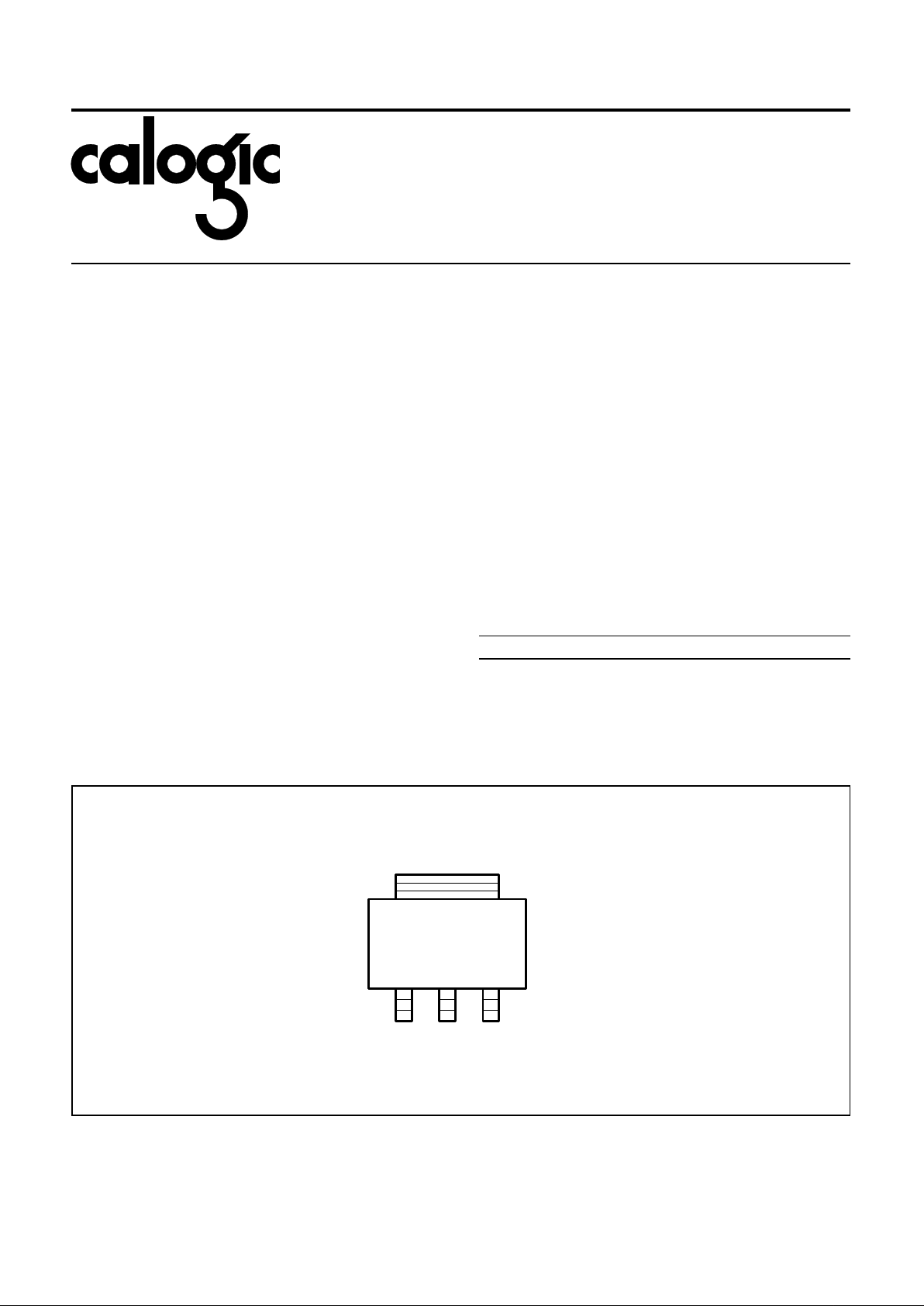
•• Surface Mou nt Packag e SO T-223
APPLICATIONS
•• SCSI-II Active Termin ator
•• Portabl e/ Pal m Top / Notebo ok C om put er s
•• Battery Charger s
•• Disk Driv es
•• Portable Consumer Equipment
•• Portable I nst ru me nt atio n
•• SMPS Post-Regula tor
PRODUCT DESCRIPTION
The Calogic CLM1117 is a low power positive voltage
regulator designed to meet 800mA output current and comply
with SCSI-II specifications with a fixed output voltage of
2.85V. This device is an excellent choi ce for use i n batterypowered applications, as active terminators for the SCSI bus,
and portable computers. The CLM1117 features very low
quiescent current and very low dropout voltage of 1.2V at a
full load and lower as output current decreases. This product
is available as an adjustable or fixed 2.85V, 3V, 3.3V, and 5V
output voltages.
The device is offered in a 3-pin surface mount package
SOT-223. The output capacitor of 10µF or larger is needed
for output stability of CLM1117 as required by most of the
other regulat or circuits.
ORDERING INFORMATION
Part Package Temperature
CLM1117M SOT-223 Industrial
CLM1117M-X SOT-223 Industrial
X = Output Voltage. 5V = Standard.
Contact factory f or 2. 8 5V, 3.0 V, 3.3 V, 10V and 12V .
CORPORATION
PIN CONNECTIONS
SOT-223
TAB IS
GND
CLM1117
ADJ./GND V
OUTVIN
123
1N-12
FRONT VIEW
CALOG IC CORPOR ATION, 237 Whitney Place, Fremont, California 94539, Telephone: 510-656-2900, FAX: 510-651-3025
Page 2
ABSOLUTE MAXIMUM RATINGS
Power Dissipation . . . . . . . . . . . . . . . . . . . . . Internally Limited
Lead Temp. (Solder ing, 5 Seconds) . . . . . . . . . . . . . . . 260
o
C
Storage Temperatur e Ra nge. . . . . . . . . . . . -65
o
C to +150oC
Operating Junct ion Temperatur e Ran ge
CLM1117 . . . . . . . . . . . . . . . . . . . . . . . . . . -40
o
C to +125oC
Input V olt age . . . . . . . . . . . . . . . . . . . . . . . . . . . . . . 2.5V to 6V
Input Supply Vo ltag e . . . . . . . . . . . . . . . . . . . . . . -20V to +20V
ESD Rating . . . . . . . . . . . . . . . . . . . . . . . . . . . . . . . . 2KV Min
CLM1117
CALOG IC CORPOR ATION, 237 Whitney Place, Fremont, California 94539, Telephone: 510-656-2900, FAX: 510-651-3025
CORPORATION
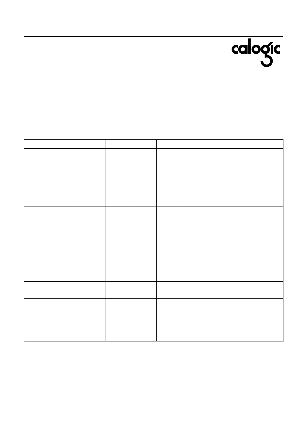
ELECTRICAL CHARACTERISTICS: VIN = V
OUT
+1, TA = 25oC, CL = 3.3µf, unless otherwise noted. Boldface apply over full
operating temperature range.
PARAMETER TYP MIN MAX UNITS CONDITIONS
Output Voltage
2.85
2.85
2.85
3.0
3.0
3.30
3.30
5.0
5.0
2.82
2.79
2.79
2.97
2.94
3.27
3.24
4.95
4.90
2.88
2.91
2.91
3.03
3.06
3.33
3.36
5.05
5.10
V
I
OUT
= 10mA, IIN = 4.8 5V
0 ≤ I
OUT
≤ 800mA, 4.25 ≤ VIN ≤ 10V
0 ≤ I
OUT
≤ 500mA, VIN = 4.05V
I
OUT
= 10mA, VIN = 5.00V
0 ≤ I
OUT
≤ 800mA, 4.50 ≤ VIN ≤ 10V
I
OUT
= 10mA, IIN = 5.3 0V
0 ≤ I
OUT
≤ 800mA, 4.80 ≤ VIN ≤ 10V
I
OUT
= 10mA, IIN = 7.0 0V
0 ≤ I
OUT
≤ 800mA, 6.50 ≤ VIN ≤ 12V
Output Voltage
T emperature Stability
0.05 % (Note 1)
Line Regulation
1.00
1.00
1.00
1.00
6.00
7.00
7.00
10.00
mV
4.25V ≤ V
IN
≤ 10V, V
OUT
= 2.85, I
OUT
= 0
4.50V ≤ V
IN
≤ 12V, V
OUT
= 3.00, I
OUT
= 0
4.80V ≤ V
IN
≤ 12V, V
OUT
= 3.30, I
OUT
= 0
4.50V ≤ V
IN
≤ 15V, V
OUT
= 5.00, I
OUT
= 0
Load Regulation
1.00
1.00
1.00
1.00
10.00
12.00
12.00
15.00
mV
0 ≤ I
OUT
≤ 800mA, VIN = 4.25V, V
OUT
= 2.8 5
0 ≤ I
OUT
≤ 800mA, VIN = 4.50V, V
OUT
= 3.0 0
0 ≤ I
OUT
≤ 800mA, VIN = 4.80V, V
OUT
= 3.3 0
0 ≤ I
OUT
≤ 800mA, VIN = 6.50V, V
OUT
= 5.0 0
Dropout Voltage
(Note 2)
1.00
1.05
1.10
1.10
1.15
1.20
V
I
L
= 100m A
I
L
= 500m A
I
L
= 800m A
Quiescent Voltage 5.00 10.00 mA 4.25V ≤ V
IN
≤ 6.5V
Current Limit 800 950 1200 mA (V
IN
- V
OUT
) = 5V
Thermal Regulation 0.01 0.1 %/W 25
o
C, 30mS Pulse
Ripple Rejection 60 75 dB f
RIPPLE
= 12 0H z, (VIN - V
OUT
) = 3V, V
RIPPLE
= 1V
p-p
Long Term Stability 0.03 % 125oC, 1000Hrs
RMS Output Noiase 0.003 % % of V
OUT
, 10Hz ≤ f ≤ 10kHz
Thermal Resistance 15
o
C/WoJunction to case, at tab
Note 1: Output temperature coeffic ien t is define d as the worst case volta ge change divid ed by the total tempe rature range .
Note 2: Dropout voltage is defined as the input to output differential at which the output voltage drops 100mV below its nominal value measured
at 1V differential at very low values of programmed output voltage, the minimum input supply voltage of 2V (2.3V over temperature) must be
taken input account.
Note 3: Thermal regulation is defined as the change in output voltage at a time T after a change in power dissipation is applied,
excluding load or line regulation effect.
Page 3

APPLICATION NOTES
EXTERNAL CAPACITOR
To ensure the stability of the CLM1117 an output capacitor of
at least 10µF (tantalum) or 50µF (aluminum) is required. The
value may change based on the application requirements on
the output lo ad or te mperature range. The cap acitor equivalent
series resistance (ESR) will effect the CLM1117 stability. The
value of the ESR can vary from the type of capacitor used in
the appli cations. The recommended value for ESR is 0.5Ω.
The output capacitance could increase in size to above the
minimum value. The larger value of output capacitance as
high as 100µF can improve the load tran sient respon se.
SOLDERING METHO D S
The CLM1 117 SOT-223 package is des igned t o be compat ible
with infrar ed refl ow or vapo r-ph ase refl ow sol dering t echniques.
During soldering the non-active or mildly active fluxes may be
used. The CLM1117 die is attached to the heatsink lead
which exits opposite the input , out put , and grou nd pins.
Hand soldering and wave soldering should be avoided since
these methods can cause damage to the device with
excessive thermal gradients on the package. The SOT-223
recommended soldering method are as follows: vapor phase
reflow and infrared reflow with the component preheated to
within 65
o
C of the soldering temper atur e rang e.
THERMAL CHARACTERISTIC S
The thermal resistance of CLM1117 is C
o
/W from junction to
tab and 31 C
o
/W from tab to ambient for a total of 46 Co/W
from junction to ambient. The CLM1117 features the internal
thermal limiting to protect the device during overload
conditions. Special care needs to be taken during continuous
load conditions to insure the maximum junction temperature
does not exceed 125
o
C.
Taking the FR-4 printed circuit board and 1/16 thick with 1
ounce copper foil as an experiment (fig.1 & fig.2), the PCB
material is effective at transmitting heat with the tab attached
to the pad area and a ground plane layer on the backside of
the substrate. Refer to table 1 for the results of the
experiment.
The thermal interaction from other components in the
application can effect the thermal resistance of the CLM1117.
The actual thermal resistance can be determined with
experimentation. CLM1117 power dissipation is calculated as
follows:
P
D
= (VIN - V
OUT
) (I
OUT
)
Maximum Junct ion Temperat ure Ra n ge:
T
J
= T
ambient
(max) + PD (thermal resistance (Junction-to-ambient))
Maximum Ju nction Temperature must not exceed 1 2 5
o
C.
P
O
= (10V - 2.85) (105mA) = (7 .15) (105mA) = 750mW
CLM1117
CORPORATION
FIGURE 1. CIRCUIT LAYOUT, THERMAL EXPERIMENTS
10V
+
10
µ
F
2.85V
27K
Ω
10µF
CLM1117 - 2.85
1N-13
CALOG IC CORPOR ATION, 237 Whitney Place, Fremont, California 94539, Telephone: 510-656-2900, FAX: 510-651-3025
FIGURE 2. SUBSTRATE LA YOUT FOR SOT-223
50 X 50mm
35 X 17mm
16 X 10mm
1N-14
T ABLE 1.
TOTAL PC BOARD AREA TOPSIDE COPPER AREA BACKSIDE COPPER AREA
THERMAL RESISTANCE
JUNCTION TO AMBIENT
2500mm
2500mm
2500mm
2500mm
2500mm
1600mm
2500mm
2500mm
1600mm
900mm
900mm
2500mm
1250mm
950mm
2500mm
1800mm
600mm
1250mm
915mm
600mm
240mm
240mm
2500mm
2500mm
2500mm
0
0
1600mm
0
0
0
900mm
0
46
o
C/W
o
47oC/W
o
49oC/W
o
51oC/W
o
53oC/W
o
55oC/W
o
58oC/W
o
59oC/W
o
67oC/W
o
72oC/W
o
85oC/W
o
Page 4

ACTIVE VS PASSI VE TERM IN ATION
The improvement in noise immunity and low quiescent power
of the terminator of less than 1W is the key advantage of
active termination compared to passive termination. The
CLM1 117 significantly improves the noise level and s ignals o n
the bus by the terminating point due to variations in voltage at
the terminat io n point due to var iat ion in th e V
term
power line.
Another advantage of active ter minat ion is t he im provem ent in
the impedance matching. The low impedance of the device
makes the termination res istance more closely m atched to th e
impedance of the cable. This improvement increases the
data rate by 10 times, from 1mbyte/s to 10mbyte/s. The
CLM1117 increases the protection and the reliability of the
application since it features internal current limiting,
overvoltage pr ot ect ion, and thermal protection.
CLM1117
ACTIVE TERMINATION CONFIGURATION
5V
IN5817
TERMPWR
CLM1117-2.85
10
µ
F
2.85V
110K
Ω
+
6 METERS MAX
10µF
5V
IN5817
CLM1117-2.85
10
µ
F
2.85V
110K
Ω
+
10µF
110K
Ω
6 METERS MAX
110K
Ω
110K
Ω
110K
Ω
UP TO 27 LINES
+ +
1N-15
CORPORATION
Information furni shed by Calogic is believed to be accurate and reliable. Howeve r, no responsibility is assumed for its use: no r for any infring eme nt of patents or other
rights of third parties which may result from its use. No license is granted by implication or otherwise under any patent rights of Calogic.
CALOG IC CORP OR ATION, 237 Whitney Place, Fremont, California 94539, Telephone: 510-656-2900, FAX: 510-651-3025
 Loading...