

Page 1
Features
■
41MSPS
■
Wide dynamic range
SFDR: 72dBc
SNR: 64dB
■
Low power dissipation: 660mW
■
Ground centered,
DC-coupled analog input
■
Excellent PSRR: >60dB
■
Very small package: 28-pin SSOP
■
Low cost
Applications
■
Cellular base-stations
■
Digital communications
■
Infrared/CCD imaging
■
IF sampling
■
Electro-optics
■
Instrumentation
■
Medical imaging
■
High definition video
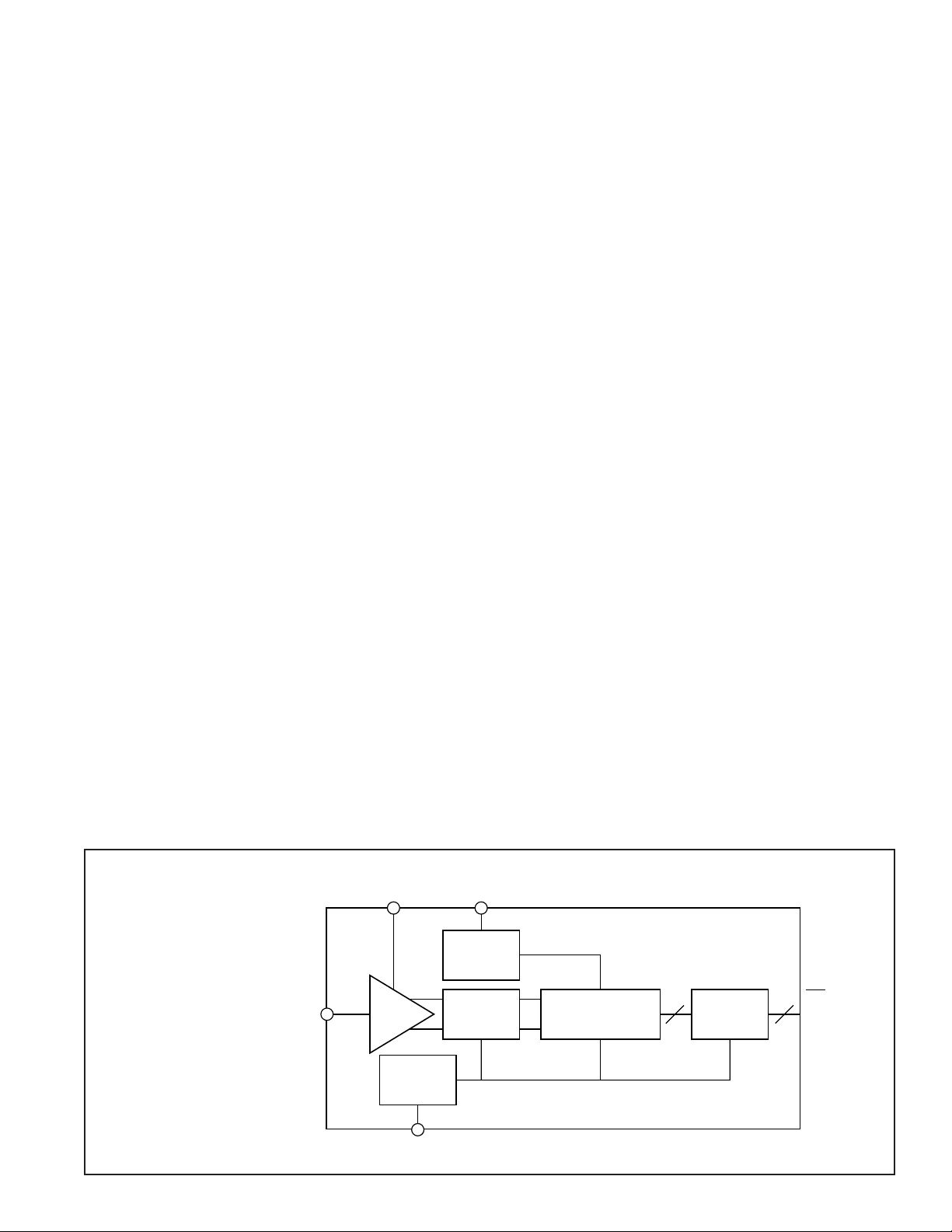
General Description
The CLC952 is a complete monolithic 12-bit 41MSPS analog-todigital converter system. Fabricated from a 0.8µm BiCMOS
process, the CLC952’s on-chip features include a very
linear wideband track-and-hold, bandgap voltage reference and a
proprietary 12-bit multi-stage quantizer. The CLC952 has been
designed for wideband digital communications receivers and
features a 72dBc spurious-free dynamic range (SFDR) and 64dB
signal-to-noise ratio (SNR).
The CLC952 operates from a standard ±5V power supply and
features excellent noise isolation with its >60dB power-supply
rejection ratio (PSRR). All digital control functions and output
registers are TTL compatible. The CLC952AC operates over the
commercial temperature range (0°C to 70°C), and the CLC952AJ
operates over the industrial temperature range (-40°C to 85°C)
version. The CLC952 is available in a 28-pin SSOP that provides
an extremely small footprint for reduced board space. National
Semiconductor thoroughly tests each part to verify full
compliance with guaranteed specifications.
CLC952
12-bit, 41MSPS Monolithic A/D Converter
N
September 1997
CLC952
12-bit, 41MSPS Monolithic A/D Converter
12-bit Subranging
Quantizer
T/H
Amplifier
TTL Output
Buffer
Timing
Generator
2.4V Voltage
Reference
Input
Amp
D11 MSB
•
•
D0 LSB
V
in
V
REF
Offset
Adjust
ENCODE
© 1997 National Semiconductor Corporation http://www.national.com
Printed in the U.S.A.
CLC952
Block Diagram
Page 2
http://www.national.com 2
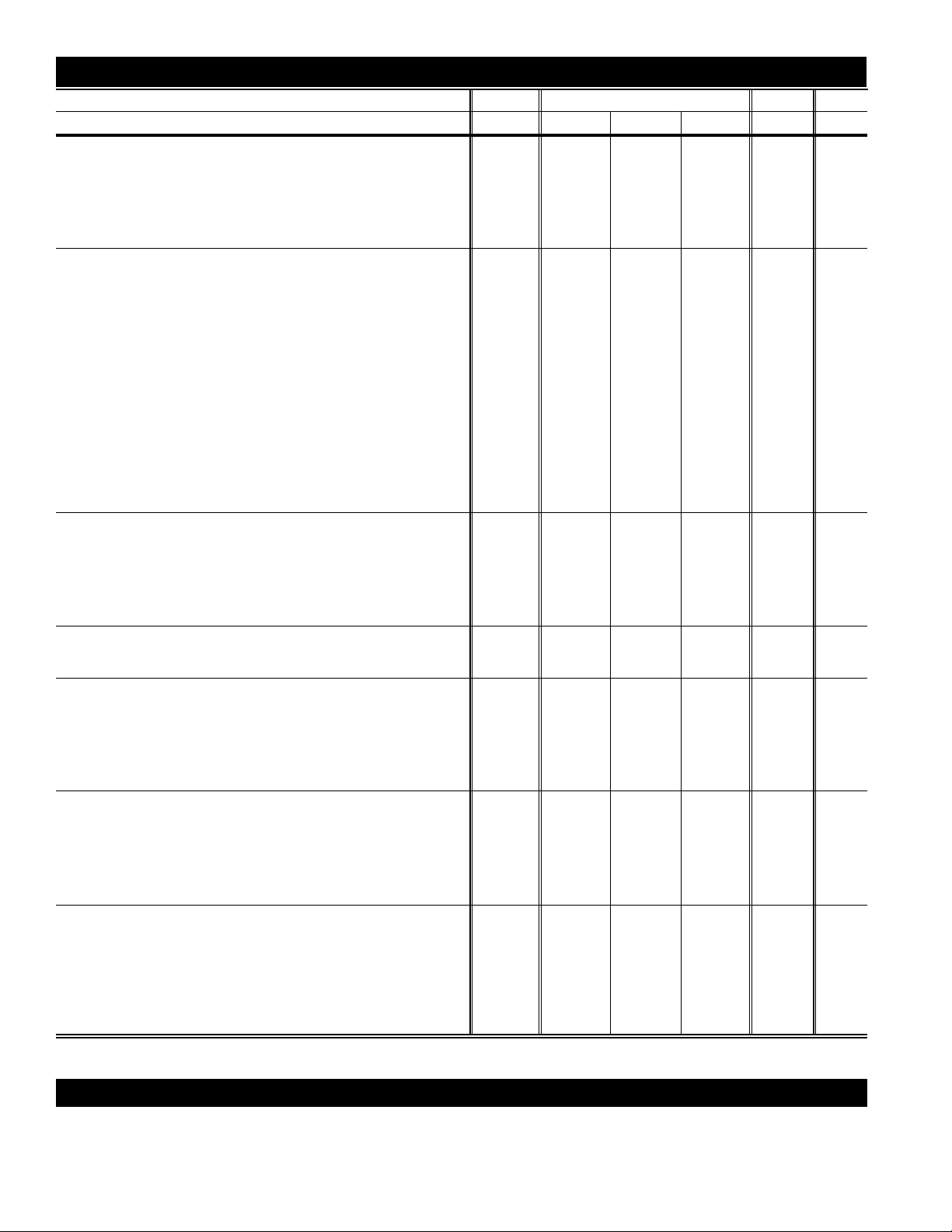
PARAMETERS CONDITIONS TEMP RATINGS UNITS NOTES
Note 4 MIN TYP MAX
DYNAMIC PERFORMANCE
small-signal bandwidth V
in
= 1/4FS +25°C 185 MHz
large-signal bandwidth V
in
= FS +25°C 180 MHz
slew rate +25°C 357 V/µs
overvoltage recovery time V
in
= 1.5FS (0.01%) +25°C 5 ns
effective aperture delay +25°C 1.6 ns
aperture jitter +25°C 4 ps(rms)
NOISE AND DISTORTION (40.96MSPS)
signal-to-noise ratio (w/o harmonics)
2.0MHz FS +25°C 60 64 dB 1
FS Full 61 dB
9.67MHz FS +25°C 60 64 dB 1
FS Full 61 dB
19.5MHz FS +25°C 60 62 dB 1
FS Full 60 dB
spurious-free dynamic range
2.0MHz FS-1dB +25°C 64 72 dBc 1
FS-1dB Full 71 dBc
9.67MHz FS-1dB +25°C 61 69 dBc 1
FS-1dB Full 68 dBc
19.5MHz FS-1dB +25°C 60 67 dBc 1
FS-1dB Full 66 dBc
intermodulation distortion
19.49MHz (f
1
), 19.9MHz (f2) FS-7dB +25°C 75 dBFS
DC ACCURACYAND PERFORMANCE
differential non-linearity DC; FS +25°C 1.4 LSB
integral non-linearity DC; FS +25°C 3.0 LSB
bipolar offset error +25°C 5.1 mV
bipolar offset error Full 25.0 mV 3
bipolar gain error +25°C -4.5 %FS
bipolar gain error Full 15.0 %FS 3
ANALOG INPUT AND PERFORMANCE
analog input resistance +25°C 500 Ω
analog input capacitance +25°C 2 pF
DIGITAL INPUTS
input voltage logic LOW Full 0.8 V 1,3
logic HIGH Full 2.0 V 1,3
input current logic LOW Full 0 5 µA 1,3
logic HIGH Full 4.0 25 µA 1,3
output voltage logic LOW Full 0.8 V 1,3
logic HIGH Full 2.4 V 1,3
TIMING
maximum conversion rate Full 40.96 MSPS 1,3
minimum conversion rate Full 3.0 MSPS 3
pulse width high Full 12.2 15 ns 3
pulse width low Full 10.5 12.2 ns 3
pipeline delay Full 1.0 clk cycle 3
output propagation delay +25°C 15 ns
POWER REQUIREMENTS
+5V supply current 41MSPS +25°C 54 70 mA 1
+5V supply current 41MSPS Full 70 mA 3
-5V supply current 41MSPS +25°C 78 100 mA 1
-5V supply current 41MSPS Full 100 mA 3
nominal power dissipation 41MSPS +25°C 660 mW
V
EE
power supply rejection ratio +25°C 72 dB
V
CC
power supply rejection ratio +25°C 60 dB
Min/max ratings are based on product characterization and simulation. Individual parameters are tested as noted. Outgoing quality levels are
determined from tested parameters.
CLC952 Electrical Characteristics
(VCC= +5V, VEE= -5V, 40.96MSPS; unless specified)
Notes
1) These parameters are 100% tested at 25°C.
2) Typical specifications are the mean values of the distributions of
deliverable converters tested to date.
3) Min/max data over temperature is based on the 5 sigma limit for
deliverable converters tested to date.
4) Full temperature range is 0°C to +70°C for AC, -40°C to +85°C for AJ.
Page 3

Absolute Maximum Ratings
positive supply voltage (VCC) -0.5V to +6V
negative supply voltage (VEE) +0.5V to -6V
differential voltage between any two grounds <200mV
analog input voltage range V
EE
toV
CC
digital input voltage range -0.5V to +V
CC
output short circuit duration (one-pin to ground) infinite
junction temperature 175°C
storage temperature range -65°C to 150°C
lead solder duration (+300°C) 10sec
Note: Absolute maximum ratings are limiting values, to be applied individually,
and beyond which the serviceability of the circuit may be impaired. Functional
operability under any of these conditions is not necessarily implied. Exposure to
maximum ratings for extended periods may affect device reliability.
Recommended Operating Conditions
positive supply voltage (VCC) +5V ±5%
negative supply voltage (VEE) -5V ±5%
differential voltage between any two grounds <10mV
analog input voltage range ±0.5V
operating temperature range (AC) 0°C to +70°C
operating temperature range (AJ) -40°C to +85°C
Package Thermal Resistance
Package θ
JA
θ
JC
28-pin SSOP 80°C/W 32°C/W
Reliability Information
Transistor count 3000
Ordering Information
Model Temperature Range Description
CLC952ACMSA 0°C to +70°C 28-pin SSOP (commercial part)
CLC952AJMSA -40°C to +85°C 28-pin SSOP (industrial part)
CLC952PCASM Fully loaded evaluation board with CLC952 … ready for test.
3 http://www.national.com
N-2 N-1 N
N N+1 N+2
N+1
N
Analog
Input
ENCODE
Digital
Outputs
(D11– D0)
tA = 1.6ns
t
OD
= 15ns typ.
N+2
CLC952 Timing Diagram
Page 4

http://www.national.com 4
Single Tone Output Spectrum
Amplitude (dBFS)
Frequency (MHz)
0
-20
-40
-60
-80
-100
0 4 8 12 16 20
40.96MSPS
A
IN
= 0.41MHz
CLC952 Typical Performance Characteristics
(VCC= +5V,VEE= -5V)
Single Tone Output Spectrum
Amplitude (dBFS)
Frequency (MHz)
0
-20
-40
-60
-80
-100
0 4 8 12 16 20
40.96MSPS
A
IN
= 4.99MHz
Single Tone Output Spectrum
Amplitude (dBFS)
Frequency (MHz)
0
-20
-40
-60
-80
-100
0 4 8 12 16 20
40.96MSPS
A
IN
= 9.67MHz
Single Tone Output Spectrum
Amplitude (dBFS)
Frequency (MHz)
0
-20
-40
-60
-80
-100
0 3 6 8 12 15
30.72MSPS
A
IN
= 0.39MHz
SFDR & SNR vs. Input Amplitude
SFDR (dBc) & SNR (dB)
Input Amplitude (dBFS)
80
70
60
50
40
30
20
10
-50 -40 -30 -20 -10 0
SFDR
SNR
Sample Rate = 40.96MSPS
A
IN
= 0.41MHz
SFDR & SNR vs. Input Amplitude
SFDR (dBc) & SNR (dB)
Input Amplitude (dBFS)
80
70
60
50
40
30
20
10
-50 -40 -30 -20 -10 0
SFDR
SNR
Sample Rate = 40.96MSPS
A
IN
= 4.99MHz
Page 5

5 http://www.national.com
SFDR & SNR vs. Input Amplitude
SFDR (dBc) & SNR (dB)
Input Amplitude (dBFS)
80
70
60
50
40
30
20
10
-50 -40 -30 -20 -10 0
SFDR
SNR
Sample Rate = 40.96MSPS
A
IN
= 9.67MHz
CLC952 Typical Performance Characteristics
(VCC= +5V,VEE= -5V)
SFDR & SNR vs. Input Amplitude
SFDR (dBc) & SNR (dB)
Input Amplitude (dBFS)
80
70
60
50
40
30
20
-50 -40 -30 -20 -10 0
SFDR
SNR
Sample Rate = 30.72MSPS
A
IN
= 7.37MHz
SFDR & SNR vs. Sample Rate
SFDR (dBc) & SNR (dB)
Sample Rate (MSPS)
90
80
70
60
50
40
0 10 20 30 40 50 60
SFDR
SNR
FS – 1dB
A
IN
= 0.41MHz
SFDR & SNR vs. Sample Rate
SFDR (dBc) & SNR (dB)
Sample Rate (MSPS)
100
80
60
40
20
0
0 10 20 30 40 50 60 70
SFDR
SNR
FS – 1dB
A
IN
= 4.99MHz
SFDR & SNR vs. Sample Rate
SFDR (dBc) & SNR (dB)
Sample Rate (MSPS)
100
80
60
40
20
0
-20
0 10 20 30 40 50 60 70
SFDR
SNR
FS – 1dB
A
IN
= 9.67MHz
SFDR & SNR vs. Input Frequency
SFDR (dBc) & SNR (dB)
Input Frequency (MHz)
80
70
60
50
1 10
SFDR
SNR
40.96MSPS
Page 6

http://www.national.com 6
SFDR & SNR vs. Input Frequency
SFDR (dBc) & SNR (dB)
Input Frequency (MHz)
85
75
65
55
45
1 10
SFDR
SNR
30.72MSPS
0.1 100
CLC952 Typical Performance Characteristics
(VCC= +5V, VEE= -5V)
Two Tone Output Spectrum
Amplitude (dBFS)
Frequency (MHz)
0
-40
-100
0
5
20
-60
-80
-20
40.96MSPS
f
1
= 19.49MHz
f
2
= 19.9MHz
10 15
Symbol
Min Max Notes
A 1.73 2.00
A1 0.00 0.21
A2 1.65 1.85
b 0.20 0.40
b1 0.20 0.33
c 0.10 0.22
c1 0.10 0.18
D 10.07 10.33 2
E 7.50 7.90
E1 5.20 5.38 2
e 0.65 BSC
L 0.52 0.95
L1 1.25 REF
R1 0.09
Notes:
1. All dimensions are in millimeters
2. Dimensions D and E1 do not include mold protrusion. Allowable protrusion is 0.20mm per side.
1
14
28
15
b
A2
A
INDEX MARK
E1E
D
e
SEE DETAIL "A"
DETAIL A
A
A
L
L1
R1
SECTION A – A
b
b1
c1
c
A1
Physical Dimensions
Page 7

AGND (Pins 1, 6, 13) Analog circuit ground.
AV
CC
(Pins 2, 12, 14) +5V power supply for the analog section. Bypass to analog ground with a 0.1µF capacitor.
AV
EE
(Pins 3, 5, 7,11) -5V power supply for the analog section. Bypass to analog ground with a 0.1µF capacitor.
ENCODE (Pin 4) ENCODE initiates a new data conversion cycle on each rising edge. Logic for this input is
standard TTL. 50% duty cycle is recommended for full compliance with the guaranteed specifications.
AIN (Pin 8) Ground-centered, DC-coupled analog input with a 1Vppmaximum input range from -0.5V to
+0.5V. Analog input impedance is approximately 500Ω.
V
OFFSET
(Pin 9) Voltage offset control. Sets the midpoint of the analog input range. Normally left floating. Ratio
of applied voltage to effective offset is 200:1. (1V applied to V
OFFSET
produces 5mV midpoint offset.)
V
REF
(Pin 10) Internal voltage reference. Nominally +2.4V. V
REF
can be pulled up or down with a voltage
source to program gain and input range. Bypass V
REF
to ground with a 0.1µF capacitor.
DV
CC
(Pin 15) +5V power supply for the digital section. Bypass to digital ground with a 0.1µF capacitor.
DGND (Pin 16) Digital ground.
D0-D11
___
(Pins 17-28) Digital data outputs are CMOS and TTL compatible. D0 is the LSB and D11
___
is the MSB.
MSB is inverted. Output coding is two’s complement.
1AGND 28 D11 (MSB INV)
2AV
CC
27 D10
3AV
EE
26 D9
4ENCODE 25 D8
5AV
EE
24 D7
6AGND 23 D6
7AV
EE
22 D5
8AIN 21 D4
9V
OFFSET
20 D3
10V
REF
19 D2
11AV
EE
18 D1
12AV
CC
17 D0 (LSB)
13AGND 16 DGND
14AV
CC
15 DV
CC
CLC952
CLC952 Pin Definitions
7 http://www.national.com
Page 8

http://www.national.com 8 Lit #150952-003
CLC952
12-bit, 41MSPS Monolithic A/D Converter
Customer Design Applications Support
National Semiconductor is committed to design excellence. For sales, literature and technical support, call the
National Semiconductor Customer Response Group at 1-800-272-9959 or fax 1-800-737-7018.
Life Support Policy
National’s products are not authorized for use as critical components in life support devices or systems without the express written approval
of the president of National Semiconductor Corporation. As used herein:
1. Life support devices or systems are devices or systems which, a) are intended for surgical implant into the body, or b) support or
sustain life, and whose failure to perform, when properly used in accordance with instructions for use provided in the labeling, can
be reasonably expected to result in a significant injury to the user.
2. Acritical component is any component of a life support device or system whose failure to perform can be reasonably expected to
cause the failure of the life support device or system, or to affect its safety or effectiveness.
National Semiconductor National Semiconductor National Semiconductor National Semiconductor
Corporation Europe Hong Kong Ltd. Japan Ltd.
1111 West Bardin Road Fax: (+49) 0-180-530 85 86 13th Floor, Straight Block Tel: 81-043-299-2309
Arlington, TX 76017 E-mail: europe.support.nsc.com Ocean Centre, 5 Canton Road Fax: 81-043-299-2408
Tel: 1(800) 272-9959 Deutsch Tel: (+49) 0-180-530 85 85 Tsimshatsui, Kowloon
Fax: 1(800) 737-7018 English Tel: (+49) 0-180-532 78 32 Hong Kong
Francais Tel: (+49) 0-180-532 93 58 Tel: (852) 2737-1600
Italiano Tel: (+49) 0-180-534 16 80 Fax: (852) 2736-9960
National does not assume any responsibility for use of any circuitry described, no circuit patent licenses are implied and National reserves the right at any time without notice to change said
circuitry and specifications.
N
 Loading...