

Page 1
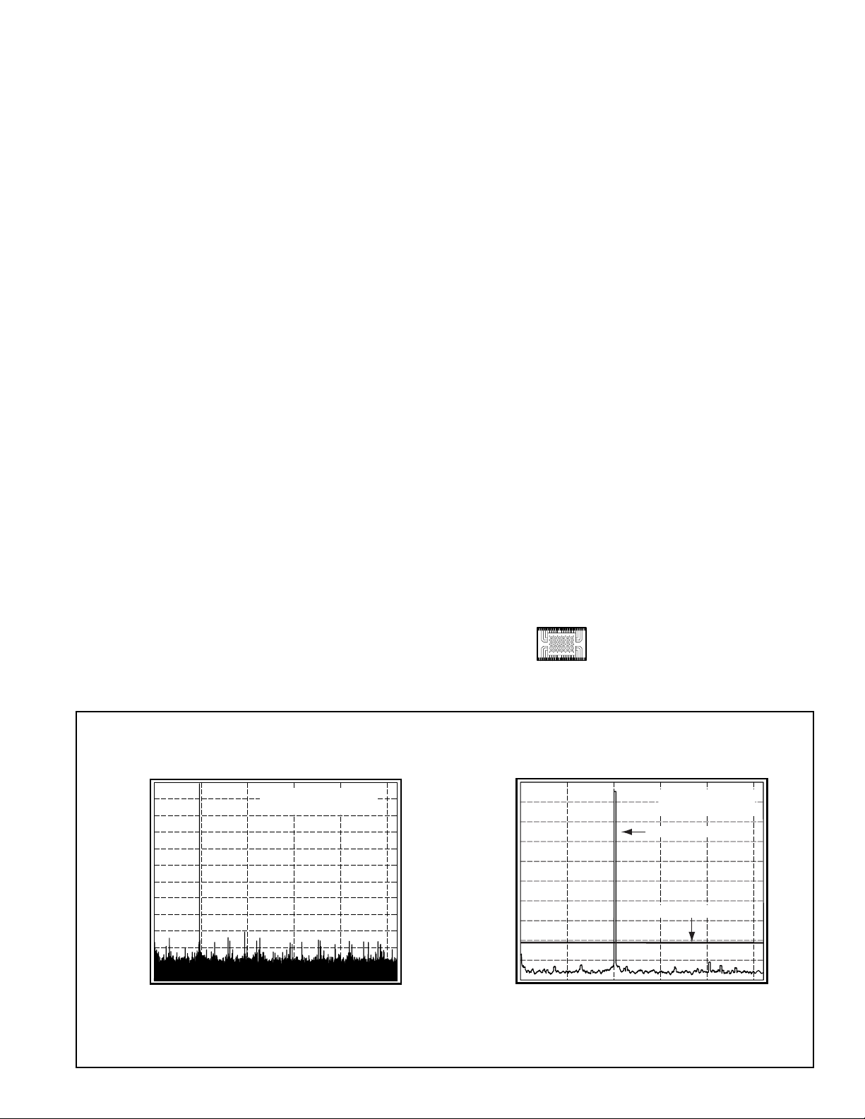
Output Response with GSM 1800 Blocker
Power at the Antenna (dBm)
Frequency (MHz)
-20
-40
-60
-80
-100
-120
0
5
25
10
15
20
Full Scale = -24dBM
Res. BW = 200KHz
-25dBm blocker
-101dBm reference
N
CLC5958
14-bit, 52MSPS A/D Converter
September 1999
CLC5958
14-bit, 52MSPS A/D Converter
General Description
The CLC5958 is a monolithic 14-bit, 52MSPS analog-to-digital
converter. The ultra-wide dynamic range and high sample rate of
the device make it an excellent choice for wideband receivers
found in multi-channel basestations. The CLC5958 integrates a
low distortion track-and-hold amplifier and a 14-bit multi-stage
quantizer on a single die. Other features include differential
analog inputs, low jitter differential clock inputs, an internal
bandgap voltage reference, and CMOS/TTL compatible outputs.
The CLC5958 is fabricated on the National ABIC-V 0.8 micron
BiCMOS process.
The CLC5958 features a 90dB spurious free dynamic range
(SFDR) and a 70dB signal to noise ratio (SNR). The balanced
differential analog inputs ensure low even-order distortion, while
the differential clock inputs permit the use of balanced clock signals
to minimize clock jitter. The 48-pin CSP package provides an
extremely small footprint for applications where space is a critical
consideration. The package also provides a very low thermal
resistance to ambient. The CLC5958 may be operated with a
single +5V power supply. Alternatively, an additional supply may
be used to program the digital output levels over the range of
+3.3V to +5V. Operation over the industrial temperature range of
-40°C to +85°C is guaranteed. National Semiconductor tests
each part to verify compliance with the guaranteed specifications.
Features
• 14-bit
• 52MSPS
• Ultra-wide dynamic range
Noise floor: -72dBFS
SFDR: 90dB
• Excellent performance to Nyquist
• IF sampling capability
• Very small package: 48-pin CSP
• Programmable output levels:
3.3V to 5V
Applications
• Multi-channel basestations
• Multi-standard basestations:
GSM, WCDMA, DAMPS, etc.
• Smart antenna systems
• Wireless local loop
• Wideband digital communications
Actual Size
(Bottom View)
Single-Tone Output Spectrum
0
-20
© 1999 National Semiconductor Corporation http://www.national.com
Printed in the U.S.A.
-40
-60
-80
Power (dBFS)
-100
-120
0
5
Frequency (MHz)
Sample Rate = 52MSPS
Input Frequency = 5MHz
10
15
20
25
Page 2
Ω
µ
µ
CLC5958 Electrical Characteristics
(V
= +5V, DV
cc
= +3.3V, 52MSPS; unless specified, T
cc
= -40°C, T
min
= +85°C)
max
PARAMETERS CONDITIONS TEMP RATINGS UNITS NOTES
MIN TYP MAX
RESOLUTION
DIFF. INPUT VOLTAGE RANGE
MAXIMUM CONVERSION RATE
SNR
SFDR
SFDR EXCLUDING 2nd & 3rd HARM. f
NO MISSING CODES
f
= 10MHZ, A
in
f
= 10MHZ, A
in
= 10MHZ, A
in
f
= 10MHZ, A
in
= -0.6dBFS +25°C 69 71 dBFS 1
in
= -0.6dBFS +25°C 80 90 dB 1
in
= -0.6dBFS +25°C 85 92 dB 1
in
= -0.6dBFS +25°C Guaranteed 1
in
Full 14 Bits 1
Full 2.048 V
Full 52 65 MSPS 1
NOISE AND DISTORTION
noise floor 2
f
= 5MHz A
in
f
= 5MHz A
in
= -1dBFS +25°C -71.0 dBFS
in
= -20dBFS +25°C -72.0 dBFS
in
2nd & 3rd harmonic distortion (w/o dither)
= 5MHz A
f
in
f
= 20MHz A
in
f
= 70MHz A
in
= -1dBFS +25°C -90 dBFS
in
= -1dBFS +25°C -87 dBFS
in
= -3dBFS +25°C -78 dBFS
in
next worst harmonic distortion (w/o dither) 3
= 5MHz A
f
in
f
= 20MHz A
in
f
= 70MHz A
in
= -1dBFS +25°C -92 dBFS
in
= -1dBFS +25°C -90 dBFS
in
= -3dBFS +25°C -90 dBFS
in
worst harmonic distortion (with dither) 4
= 5MHz A
f
in
f
= 20MHz A
in
f
= 70MHz A
in
f
= 70MHz (2nd & 3rd excluded) A
in
= -6dBFS +25°C -95 dBFS
in
= -6dBFS +25°C -95 dBFS
in
= -6dBFS +25°C -82 dBFS
in
= -6dBFS +25°C -95 dBFS
in
2-Tone IM distortion (w/o dither)
f
=12MHz, f
in1
= 15MHz A
in2
in1
= A
= -7dBFS +25°C -100 dBFS
in2
SINAD (w/o dither)
= 5MHz A
f
in
= -1dBFS +25°C 69 dB
in
CLOCK RELATED SPURIOUS TONES
fs/8, fs/4 +25°C -95 dBFS
next worst clock spur +25°C -100 dBFS 5
calibration sideband coefficient +25°C 100e-6 6
DC ACCURACY AND PERFORMANCE
differential non-linearity +25°C ±0.3 LSB
integral non-linearity +25°C ±1.5 LSB
offset error +25°C ±2.0 mV
gain error +25°C 2 % of FS
DYNAMIC PERFORMANCE
large-signal bandwidth +25°C 210 MHz
aperture jitter +25°C 0.5 ps(rms)
TIMING
effective aperture delay (t
pipeline delay (t
) Full 3 clk cycle
P
output buffer delay (t
data valid buffer delay (t
) +25°C -0.2 ns
A
) +25°C 6.6 ns
o
) +25°C 6.6 ns
DAV
ANALOG INPUT CHARACTERISTICS
single-ended input resistance +25°C 500
single-ended capacitance +25°C 3.6 pF
ENCODE INPUT CHARACTERISTICS
VIH Full 3.9 4.5 V 7
VIL Full 3.0 3.8 V 7
differential input swing Full 0.2 V
IIL Full 2
IIH Full 25
A
A
Min/max ratings are based on product characterization and simulation. Individual parameters are tested as noted. Outgoing quality levels are
determined from tested parameters.
http://www.national.com
2
Page 3
CLC5958 Electrical Characteristics
(V
= +5V, DV
cc
= +3.3V, 52MSPS; unless specified, T
cc
= -40°C, T
min
= +85°C)
max
PARAMETERS CONDITIONS TEMP RATINGS UNITS NOTES
MIN TYP MAX
DIGITAL OUTPUT CHARACTERISTICS
VOH IOH = 50 µ A Full 3.2 V
VOL IOL = 50 µ A Full 0.1 V
SUPPLY CHARACTERISTICS
+5V supply current (V
+3.3V supply current (DV
) +25°C 260 300 mA 1
CC
) +25°C 32 40 mA 1
CC
power dissipation +25°C 1.4 W
power supply rejection ratio +25°C 0.75 mV/V
V
CC
Min/max ratings are based on product characterization and simulation. Individual parameters are tested as noted. Outgoing quality levels are
determined from tested parameters.
CLC5958 Timing Diagram
1) These parameters are 100% tested at 25°C.
2) Harmonics and clock spurious are removed in noise
measurements.
3) 4th or higher harmonic.
4) Low frequency dither injected in the DC to 500KHz band.
5) Next worst clock spur is a subharmonic of fs, but not fs/8 or fs/4.
See text on spurious.
N + 1
Notes
6) See text on calibration sidebands in the application
information section.
7) Encode levels are referenced to V
1.1V below V
, and the maximum VIH value is 0.5V below V
CC
, i.e. the minimum VIH value is
CC
CC
.
Analog
Input
t
A
ENCODE
Data
DAV
N
N-3
t
O
t
DAV
N+1
N-2
N+2
CLC5958 Timing Diagram
Absolute Maximum Ratings
positive supply voltage (V
differential voltage between any two grounds <200mV
analog input voltage range GND to V
digital input voltage range -0.5V to +V
output short circuit duration (one-pin to ground) infinite
junction temperature 175°C
storage temperature range -65°C to 150°C
lead solder duration (+240°C) 5sec
Note: Absolute maximum ratings are limiting values , to be applied individually, and
beyond which the serviceability of the circuit may be impaired. Functional
operability under any of these conditions is not necessarily implied. Exposure to
maximum ratings for extended periods may affect device reliability.
) -0.5V to +6V
CC
CC
CC
tO: Delay from rising edge of
ENCODE to output data
transition – nominally 6.6ns
: Delay from falling edge of
t
DAV
ENCODE to rising edge of DAV
– nominally 6.6ns
: Effective aperture delay
t
A
– nominally -0.2ns
N-1
N+3
N
Recommended Operating Conditions
positive supply voltage (V
analog input voltage range 2.048V
input coupling AC
operating temperature range -40°C to +85°C
digital output supply voltage (DV
analog input common mode voltage V
) +5V ±5%
CC
) +3.3V ±5%
CC
±0.025V
cm
diff.
pp
Pac kage Thermal Resistance
Package
48-pin CSP 39°C/W 5°C/W
θ
JA
θ
JC
Pac kage Transistor Count
Transistor count 10,000
Ordering Information
Model Temperature Range Description
CLC5958SLB -40°C to +85°C 48-pin CSP (industrial temperature range)
CLC5958PCASM Fully loaded evaluation board with CLC5958 … ready for test.
3
http://www.national.com
Page 4
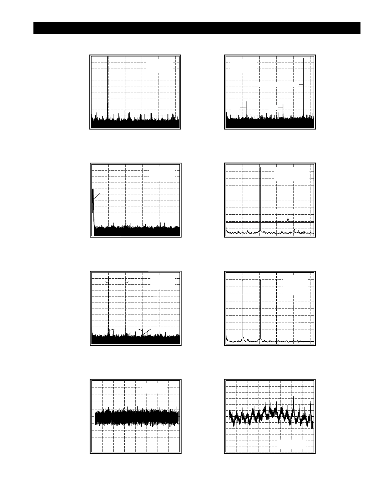
CLC5958 Typical Performance Characteristics
(V
= +5V, 52MSPS; unless specified)
cc
Single-Tone Output Spectrum
0
-20
-40
-60
-80
Power (dBFS)
-100
-120
0
10
5
Fs = 52MSPS
F
in
A
in
15
= 5MHz
= -0.6dBFS
20
-20
-40
-60
-80
Power (dBFS)
-100
-120
25
Frequency (MHz)
Single-Tone Output Spectrum (w/Dither)
0
-20
-40
Dither
-60
-80
Power (dBFS)
-100
Fs = 52MSPS
F
= 10MHz
in
A
= -6dBFS
in
-20
-40
-60
-80
-100
Power at the Antenna (dBm)
-120
10
15
0
5
20
25
-120
Frequency (MHz)
Single-Tone Output Spectrum
0
Fs = 52MSPS
F
= 75MHz
in
A
= -3.2dBFS
in
Fundamental = 75MHz
2nd
0
5
3rd
10
15
Frequency (MHz)
Single-Tone Output Spectrum
w/200KHz Res. BW
Full Scale = -24dBm
F
= 10MHz
in
A
= -25dBm
in
-101dBm reference
10
0
5
15
Frequency (MHz)
20
25
20
25
Two-Tone Output Spectrum
0
-20
f1
-40
-60
-80
Power (dBFS)
-100
f2-f1
-120
0
5
Frequency (MHz)
Differential Non-Linearity
1.0
0.6
0.2
LSBs
-0.2
-0.6
-1.0
0
4000
10
f2
f1+f2
8000
Code
Fs = 52MSPS
f
= 5MHz
1
f
= 10MHz
2
2f2-f1
15
Fs = 52MSPS
F
= 4.9791
in
12000 16000
Two-Tone Output Spec. w/200KHz Res. BW
-20
-40
-60
-80
-100
F
= 5MHz
in1
F
= 10MHz
in2
A
= -31dBm
in1
A
= -31dBm
in2
Power at the Antenna (dBm)
20
25
0
-120
10
15
5
20
25
Frequency (MHz)
Integral Non-Linearity
3.0
2.0
1.0
0
LSBs
-1.0
-2.0
-3.0
0
4000
8000
Fs = 52MSPS
F
= 4.9791MHz
in
12000 16000
Code
http://www.national.com
4
Page 5

CLC5958 Typical Performance Characteristics
(V
= +5V, 52MSPS; unless specified)
cc
Noise and Spurious
vs. Amplitude at F
120
110
Other Spurious
100
90
-dBFS
80
Noise Floor
70
60
-60 -50
-70
Noise and Spurious
vs. Amplitude at F
120
110
100
90
-dBFS
Other Spurious
80
Noise Floor
70
60
-60 -50 -40
-70
= 10MHz
in
Fs/8 or Fs/4
2nd or 3rd Harmonic
-30
-40
Amplitude (dBFS)
= 75MHz
in
2nd or 3rd Harmonic
-30
Amplitude (dBFS)
Fs = 52MSPS
-10
-20
Fs = 52MSPS
Fs/8 or Fs/4
-20 -10
Spurious vs. Amplitude
with Dither at F
120
110
= 10MHz
in
2nd or 3rd Harmonic
100
90
-dBFS
Other Spurious
Fs/8 or Fs/4
80
70
Fs = 52MSPS
60
-20 -10
-60 -50 -40
0
-70
-30
0
Amplitude (dBFS)
Spurious vs. Amplitude
with Dither at F
120
110
= 75MHz
in
2nd or 3rd Harmonic
100
90
-dBFS
Other Spurious
Fs/8 or Fs/4
80
70
Fs = 52MSPS
60
-10
-20
-60 -50 -40
0
-70
-30
0
Amplitude (dBFS)
Noise and Distortion vs. Sample Rate
120
110
100
2nd or 3rd Harmonic
90
dBFS
80
70
Noise Floor
Other Spurious
60
50
40
10 20
30
Sample Rate (MSPS)
Noise and Spurious vs. Input Frequency
120
110
100
Fs/8 or Fs/4
90
-dBFS
80
70
2nd or 3rd Harmonic
Other Spurious
Noise Floor
60
15
10
5
0
Input Frequency (MHz)
Fin = 10MHz
A
= -0.6dBFS
in
60
Fs = 52MSPS
A
= -0.6dBFS
in
20
Clock Spurious vs. Sample Rate
120
110
fs/8
"next clock spurs"
100
-dBFS
90
fs/4
80
70
40
70
10 20
30
Fin = 10MHz
A
= -0.6dBFS
in
50
60
70
Sample Rate (MSPS)
Noise and Spurious vs. Input Frequency
120
110
100
90
Other Spurious
Fs = 52MSPS
A
= -3.2dBFS
in
Fs/8 or Fs/4
-dBFS
80
70
Noise Floor
60
25
010
2nd or 3rd Harmonic
20
30
40
70
60
50
Input Frequency (MHz)
5 http://www.national.com
Page 6

CLC5958 Pin Definitions
1 GND
2 GND
3 GND
4 GND
5V
CC
6V
CC
7V
CC
8 GND
9 ENCODE
10 ENCODE
11 GND
12 GND
13 A
IN
14 A
IN
15 GND
16 V
CC
17 V
CC
18 V
CC
19 GND
20 GND
21 V
CM
22 V
CC
23 GND
24 GND
CLC5958
vias
GND
GND
V
CC
(MSB) D13
D12
D11
D10
D9
D8
D7
DV
CC
DV
CC
GND
GND
D6
D5
D4
D3
D2
D1
(LSB) DO
DAV
GND
GND
48
47
46
45
44
43
42
41
40
39
38
37
36
35
34
33
32
31
30
29
28
27
26
25
A
IN, AIN
(Pins 13, 14) Differential inputs. Self biased at a common
mode voltage of +3.25V. The ADC full scale input is
2.048Vpp differential.
ENCODE, (Pins 9, 10) Differential clock inputs. ENCODE initiates a
ENCODE new data conversion cycle on each rising edge. Clock
signals may be sinusoidal or square waves with PECL
encode levels. The falling edge of ENCODE clocks
internal pipeline stages.
D0-D13 (Pins 28 - 34, 39 - 45) Digital data outputs. CMOS
and TTL compatib le. D0 is the LSB and D13 is the inverted
MSB. Output coding is two’s complement.
DAV (Pin 27) Data valid. The rising edge of this signal occurs
when output data is valid and may be used to latch data
into following circuitry.
V
CM
(Pin 21) Internal analog input common mode voltage
reference. Nominally +3.25V. Can be used to establish the
analog input common mode voltage for DC coupled
applications (DC coupling not recommended, see
applications section).
GND (Pins 1 - 4, 8, 11, 12, 15, 19, 20, 23 - 26, 35, 36, 47, 48,
and vias) circuit ground.
V
CC
(Pins 5 - 7, 16 - 18, 22, 46) +5V power supply. Bypass
each group of supply pins to ground with a 0.01µF
capacitor.
AIN
ENCODE
T&H
DV
CC
(Pins 37, 38) +3.3V to +5V power supply for the digital
outputs. Establishes the high output level for the digital
outputs. Bypass to ground with a 0.1µF capacitor.
CLC5958 Block Diagram
Summing
Network
4-bit
Flash
Over-range Correction Logic & Output Buffers
4-bit
DAC
Residue
Amp
10-bit
Fine
ADC
http://www.national.com 6
Page 7

CLC5958 Package Dimensions
7 http://www.national.com
Page 8

CLC5958 Application Information
Driving the Analog Inputs
The differential analog inputs, AIN and AIN, are biased
from an internal 3.25V reference (a 2.4V bandgap
reference plus a diode) through an on-chip resistance of
500Ω. This bias voltage is set for optimum performance,
and varies with temperature. Since DC coupling the
inputs overrides the internal common mode voltage, it is
recommended that the inputs to the CLC5958 be AC
coupled whenever possible. The time constant of the
input coupling network must be greater than 1µsec to
minimize distortion due to nonlinear input bias currents.
Additionally, the common mode source impedance
should be less than 100Ω at the sample rate.
If DC coupling is required, then the V
output may be
CM
used to establish the input common mode voltage. The
CLC5958 samples the common mode voltage at the
internal track-and-hold output and servos the VCM output
to establish the optimum common mode potential at the
track-and-hold. It is possible to use the VCM output to
construct an external servo loop.
Figure 1 below illustrates one input coupling method. The
transformer provides noiseless single-ended to
differential conversion. The two 50Ω resistors in the
secondary define the input impedance and provide a low
common mode source impedance through the bypass
capacitors.
VIN
0.1
1:1.4
0.1
50
0.01
50
AIN
CLC5958
0.1
100
VIN
VIN
100
0.1
AIN
39pf
CLC5958
39pf
AIN
0.1
Figure 2: Differential Amplifier
Driving the ENCODE Inputs
The ENCODE and ENCODE inputs are differential clock
inputs that are referenced to VCC. They may be driven
with PECL input levels. Alternatively they may be driven
with a differential input (e.g. a sine input) that is centered
at 1.2 Volts below VCC and which meets the min and max
ratings for VIL and VIH. Low noise differential clock signals
provide the best SNR performance for the converter.
The ENCODE inputs are not self biasing, so a DC bias
current path must be provided to each of the inputs.
Figure 3 shows one method of driving the encode inputs.
25
MC10EL16
Q
D
Q
0.1
25
D
V
BB
ENCODE
CLC5958
ENCODE
332332
Clock
0.1
1:1
Figure 3: ENCODE Inputs
0.1
AIN
Figure 1: Input Coupling
Alternatively, the inputs can be driven using a differential
amplifier as shown in Figure 2.
The network of Figure 2 uses a simple RC low-pass filter
to roll off the noise of the differential amplifier. The network has a cutoff frequency of 40MHz. Different noise
filter designs are required for different applications. For
example, an IF application would require a band-pass
noise filter.
The analog input lines should be routed close together so
that any coupling from other sources is common mode.
http://www.national.com 8
The transformer converts the single-ended clock signal to
a differential signal. The center-tap of the secondary is
biased by the VBB potential of the ECL buffer. The diodes
in the secondary limit the input swing to the buffer.
Since the encode inputs are close to the analog inputs, it
is recommended that the analog inputs be routed on the
top of the board directly over a ground plane and that the
encode lines be routed on the back of the board and then
connected through via to the encode inputs.
Latching the Output Data
The rising edge of DAV is approximately centered in the
data transition window, and may be used to latch the
output data. The DAV output has twice the load driving
capability of the data outputs so that two latch clock
inputs may be driven by this output.
Page 9

Routing Output Data Lines
It is recommended that the ground plane be removed
under the data output lines to minimize the capacitive
loading of these lines. In some systems this may not be
permissible because of EMI considerations.
Harmonics and Clock Spurious
Harmonics are created by non-linearity in the track-andhold and the quantizer. Harmonics that arise from
repetitive non-linearities in the quantizer may be reduced
by the application of a dither signal.
Transformers and baluns can contribute harmonic
distortion, particularly at low frequencies where transformer operation relies on magnetic flux in the core. If a
transformer is used to perform single-ended to differential
conversion at the input, care should be taken in the
selection of the transformer.
The clock is internally divided by the CLC5958 in order to
generate internal control signals. These divided clocks
can contribute spurious energy , principally at fs/4 and fs/8.
The clock spurious is typically less than -90dBFS.
6
3 52e
32
6
3
=
6
7.9KHz
32 4.8671e
n round
=
f 4.8671e
=−∗=
∆
∗
52e
6
If the input is a full scale input, then the magnitude of the
sidebands is derived as:
x 1024 7.9e /52e 0.489
==
a 100e
=∗
∆
36
π
sin .489
-6 -6
()
.489
==−
96e 80dBc
The sidebands roll off rapidly with increasing sideband
offset. For example, if the sideband is offset 200KHz from
the carrier (in an adjacent GSM channel) as opposed to
the 7.9KHz offset from the previous example, the sideband magnitude is reduced to -116dBc.
Figure 4 shows how the sideband offset frequency
varies with input frequency at a sample rate of 52MSPS.
Calibration Sidebands
The CLC5958 incorporates on-board calibration. The
calibration process creates low level sideband spurious
close to the carrier and near DC for some input
frequencies. In most applications these sidebands will
not be an issue. The sidebands add negligible power to
the carrier and therefore do not reduce sensitivity in
receiver applications. Also, the sidebands never fall in
adjacent channels with any appreciable power. They may
be visible in some very narrow-band applications, and so
are documented here for completeness.
The offset of the sidebands relative to the carrier and relative to DC is derived using the equations:
n round
=
32f
in
f
s
ff
=−
∆
nf
s
in
32
where f∆ is the sideband offset, fin is the input
frequency, fs is the sample rate, and round(•) denotes
integer rounding. The magnitude of the sideband relative
to the carrier for a full scale input tone is approximated by
the equations:
sin x
x 1024 f / f a
==
πα
s
∆∆
()
x
where a∆ is the sideband magnitude relative to the input,
and α is the calibration sideband coefficient. The value of
α rolls off 2dB per dB as the input amplitude is reduced.
For example, assume the input frequency is 4.8671MHz
and the sample rate is 52MSPS. Then the sideband
offset is derived as follows:
800
700
600
500
400
(KHz)
∆
f
300
200
100
0
0
10
5
Input Frequency (MHz)
15
20
25
Figure 4: Sideband Offset vs. Input Frequency
The sideband magnitude is a function of the sideband
offset, as illustrated in Figure 5.
-80
-85
-90
-95
-100
-105
-110
-115
Sideband Magnitude (dBc)
-120
0 100 200 300 400 500 600
f∆ (KHz)
700
800
Figure 5: Sideband Magnitude vs. Sideband Offset
9 http://www.national.com
Page 10

Power Supplies
The VCC pins supply power to all of the CLC5958
circuitry with the exception of the digital output buffers.
The D VCC pins provide power to the digital output buffers.
Each supply pin should be connected to a supply (i.e. do
not leave any supply pins floating).
Local groups of supply pins should be bypassed
with.01uF capacitors. These capacitors should be placed
as close to the part as possible. Avoid using via to the
ground plane. If vias to the ground plane cannot be
avoided, then use multiple vias in close proximity to the
bypass capacitor.
The supplies should be bypassed in a manner to prevent
supply return currents from flowing near the analog
inputs. The evaluation board layout is an example of how
to accomplish this.
The digital output buffer supplies (DVCC) provide a
means for programming the output buffer high level.
Supply values ranging from 3.3V to 5.0V may be applied
to these pins. In general, best performance is achieved
with DVCC set to 3.3V.
Layout Recommendations for the CSP
The 48 lead chip scale package not only provides a small
footprint, but also provides an excellent connection to
ground. The thermal vias on the bottom of the package
also serve as additional ground pads. The solder pad
dimensions on the pc board should match the package
pads 1:1.
Soldering Recommendations for the CSP
A 4 mil thick stencil for the solder screen printing is
recommended. The suggested IR reflow profile is:
Ramp Up: 2°C/sec
Dwell Time > 183°C: 75 sec
Solder Temperature: 215°C
(max solder temperature): 235°C
Dwell Time @ Max Temp: 5 sec
Ramp Down: 2°C/sec
CLC5958 Evaluation Board
Description
The CLC5958 evaluation printed circuit board provides a
convenient test bed for rapid evaluation of the CLC5958.
It illustrates the proper approach to layout in order to
achieve best performance, and provides a performance
benchmark.
Analog Input
The CLC5958 evaluation board is configured to be driven
by a single-ended signal at the AIN SMA connector (the
AIN
connector is disconnected). The AIN SMA
connector should be driven from a 50Ω source
impedance. A full scale input is approximately 1.4V
(7dBm). The single-ended input is converted to a
differential input by an on-board transformer.
When performing sine wave testing, it is critical that the
input sine wave be filtered to remove harmonics and
source noise.
Encode Input
The CLK SMA connector is the encode input and should
also be driven from a 50Ω source. A low jitter 16dBm sine
wave should be applied at this input. In some cases it
may be necessary to band-pass filter the sine wave in
order to achieve low jitter.
pp
The single-ended clock input is converted to a differential
signal by an on-board transformer and buffered by an
ECL buffer.
Digital Outputs
The digital outputs are available at the Eurocard
connector (J1). Data bits D0 through D13
J1 pins 18B through 5B. The data ready signal (labeled
DR in the schematic) is available at J1 pin 20B. These
outputs are also available at the HP 01650-63203
termination adapter for direct connection to an HP logic
analyzer (see evaluation board schematic). The outputs
are buffered by 3.3V digital latches. The falling edge of
the data ready signal may be used to latch the output data.
Supply V oltages
Power is sourced to the board through the Eurocard connector. A 5V supply should be connected at J1 pins 32A
and 32B. A 3.3V supply should be connected at J1 pins
31A and 31 B. The ground return for these supplies is at
J1 pins 27A, 27B, 28A, and 28B. It is recommended that
low noise linear supplies be used.
are available at
http://www.national.com 10
Page 11

CLC5958 Evaluation Board Layout
CLC5958PCASM Layer 1 CLC5958PCASM Layer 2
CLC5958PCASM Layer 3 CLC5958PCASM Layer 4
11 http://www.national.com
Page 12

CLC5958 Evaluation Board Schematic
http://www.national.com 12
Page 13

CLC5958
14-bit, 52MSPS A/D Converter
Customer Design Applications Support
National Semiconductor is committed to design excellence. For sales, literature and technical support, call the
National Semiconductor Customer Response Group at 1-800-272-9959 or fax 1-800-737-7018.
Life Support Policy
National’s products are not authorized for use as critical components in lif e support devices or systems without the e xpress written approv al
of the president of National Semiconductor Corporation. As used herein:
1. Life support devices or systems are devices or systems which, a) are intended for surgical implant into the body, or b) suppor t or
sustain life, and whose failure to perform, when properly used in accordance with instructions for use provided in the labeling, can
be reasonably expected to result in a significant injury to the user.
2. A critical component is any component of a life support device or system whose failure to perform can be reasonably expected to
cause the failure of the life support device or system, or to affect its safety or effectiveness.
National Semiconductor National Semiconductor National Semiconductor National Semiconductor
Corporation Europe Hong Kong Ltd. Japan Ltd.
1111 West Bardin Road Fax: (+49) 0-180-530 85 86 13th Floor, Straight Block Tel: 81-043-299-2309
N
National does not assume any responsibility for use of any circuitry described, no circuit patent licenses are implied and National reserves the right at any time without notice to change said
circuitry and specifications.
http://www.national.com 13
Arlington, TX 76017 E-mail: europe.support.nsc.com Ocean Centre, 5 Canton Road Fax: 81-043-299-2408
Tel: 1(800) 272-9959 Deutsch Tel: (+49) 0-180-530 85 85 Tsimshatsui, Kowloon
Fax: 1(800) 737-7018 English Tel: (+49) 0-180-532 78 32 Hong Kong
Francais Tel: (+49) 0-180-532 93 58 Tel: (852) 2737-1600
Italiano Tel: (+49) 0-180-534 16 80 Fax: (852) 2736-9960
 Loading...