

Page 1

N
CLC5957
12-bit, 70MSPS Broadband Monolithic A/D Converter
October 1999
CLC5957
12-bit, 70MSPS Broadband Monolithic A/D Converter
General Description
The CLC5957 is a monolithic 12-bit, 70MSPS analog-to-digital
converter. The device has been optimized for use in IF-sampled
digital receivers and other applications where high resolution,
high sampling rate, wide dynamic range, low power dissipation,
and compact size are required. The CLC5957 features differential
analog inputs, low jitter differential universal clock inputs, a low
distortion track-and-hold with 0-300MHz input bandwidth, a bandgap voltage reference, data valid clock output, TTL compatible
CMOS (3.3V or 2.5V) programmable output logic, and a proprietary 12-bit multi-stage quantizer. The CLC5957 is fabricated on
the ABIC-V 0.8 micron BiCMOS process.
The CLC5957 features a 74dBc spurious free dynamic range
(SFDR) and a 67dB signal to noise ratio (SNR). The wideband
track-and-hold allows sampling of IF signals to greater than
250MHz. The part produces two-tone, dithered, SFDR of 83dBFS
at 75MHz input frequency. The differential analog input provides
excellent common mode rejection, while the differential universal
clock inputs minimize jitter. The 48-pin TSSOP package provides
an extremely small footprint for applications where space is a
critical consideration. The CLC5957 operates from a single +5V
power supply. Operation over the industrial temperature range of
-40°C to +85°C is guaranteed. National Semiconductor tests
each part to verify compliance with the guaranteed specifications.
Features
• 70MSPS
• Wide dynamic range
SFDR: 74dBc
SFDR w/dither: 85dBFS
SNR: 67dB
• IF sampling capability
• Input bandwidth = 0-300MHz
• Low power dissipation: 640mW
• Very small package: 48-pin TSSOP
• Single +5V supply
• Data valid clock output
• Programmable output levels:
3.3V or 2.5V
Applications
• Cellular base-stations
• Digital communications
• Infrared/CCD imaging
• IF sampling
• Electro-optics
• Instrumentation
• Medical imaging
• High definition video
ME79TG
ME79TG
ME79TG
ME79TG
CLC5957
CL5956
CL5956
CL5956
Actual Size
MTD
IMTD
IMTD
IMTD
N
N
N
N
ADC Block Diagram
3-bit
DAV
IF
Saw
IF
Input
Q
3
12
ADC
Out
~
~
BPF
(150MHz
typ.)
SINAD dBc (BW = 216KHz)
Clock
In
A
T/H
In
© 1999 National Semiconductor Corporation http://www.national.com
Printed in the U.S.A.
3-bit
Q
Single Tone Output Spectrum w/Dither
0
-10
F
-20
-30
-40
-50
-60
-70
Output Level (dBFS)
-80
-90
-100
0
3
Bit Align/Error Correct
Fin = 25.3MHZ
= 66MHz
sample
8284
Frequency (MHz)
3-bit
Q
12 16 20 24 32
3-bit
Q
3
3
First IF Receiver
DVGA
(∆G = 42dB)
Noise
BPF
3-bit (Gain Control)
Decimation/filter = 190/0.8
Output BW = 50M/190 X 0.8 = 210KHz
Receiver SINAD vs. Input Amplitude
90
80
70
60
50
40
30
20
10
0
-125
Input (dBFS)
CLC5957
12-bit
70MSPS
ADC
-50 -25 0-75-100
12
DAV
CLC5902
Dig.
Tuner/
Filter
AGC
20
Page 2
Ω
Ω
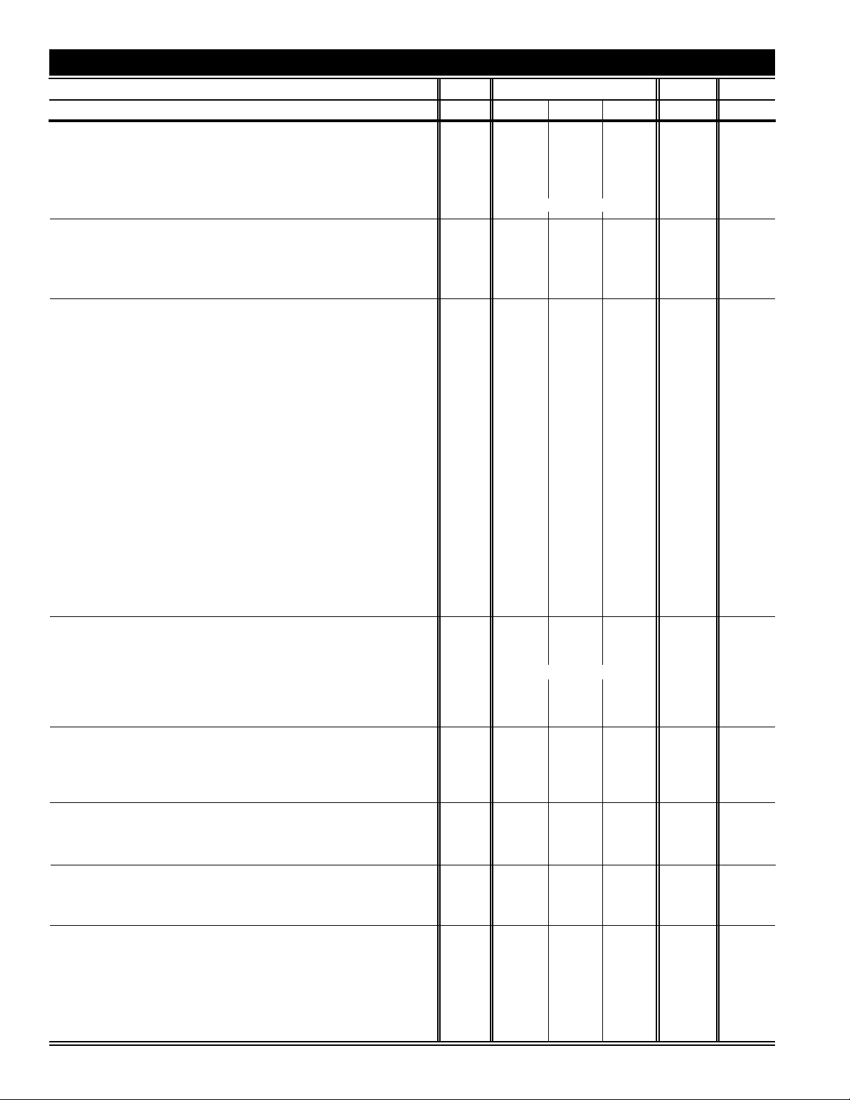
CLC5957 Electrical Characteristics
(V
= +5V, 66MSPS; unless specified) (T
cc
= -40°C, T
min
= +85°C)
max
PARAMETERS CONDITIONS TEMP RATINGS UNITS NOTES
MIN TYP MAX 2
RESOLUTION
DIFF. INPUT VOLTAGE RANGE
MAXIMUM CONVERSION RATE
SNR
SFDR
NO MISSING CODES
f
= 25MHz, A
in
f
= 25MHz, A
in
f
= 5MHz, A
in
= -1dBFS +25°C 63 66 dBFS 1
in
= -1dBFS +25°C 66 74 dBc 1
in
= -1dBFS +25°C Guaranteed 1
in
Full 12 Bits 1
Full 2.048 V
Full 70 75 MSPS 1
DYNAMIC PERFORMANCE
large-signal bandwidth A
overvoltage recovery time A
= -3dBFS +25°C 300 MHz
in
= 1.5FS (0.01%) +25°C 12 ns
in
effective aperture delay (Ta) +25°C -0.41 ns
aperture jitter +25°C 0.3 ps(rms)
NOISE AND DISTORTION
signal-to-noise ratio (w/o 50 harmonics)
f
= 5.0MHz A
in
= 25MHz A
f
in
f
= 75MHz A
in
f
= 150MHz A
in
f
= 250MHz A
in
= -1dBFS Full 67 dBFS
in
= -1dBFS Full 60 66 dBFS 1
in
= -3dBFS Full 65 dBFS
in
= -15dBFS Full 66 dBFS
in
= -15dBFS Full 66 dBFS
in
spurious-free dynamic range
= 5.0MHz A
f
in
f
= 25MHz A
in
f
= 75MHz A
in
f
= 150MHz A
in
f
= 250MHz A
in
= -1dBFS Full 74 dBc
in
= -1dBFS Full 60 74 dBc 1
in
= -3dBFS Full 72 dBc
in
= -15dBFS Full 69 dBc
in
= -15dBFS Full 65 dBc
in
intermodulation distortion
= 149.84MHz, f
f
in1
f
= 249.86MHz, f
in1
= 149.7MHz A
in2
= 249.69MHz A
in2
= -10dBFS +25°C 68 dBFS
in
= -10dBFS +25°C 58 dBFS
in
dithered performance
spurious-free dynamic range
= 19MHz A
f
in
= -6dBFS +25°C 85 dBFS
in
intermodulation distortion
f
= 74MHz, f
in1
= 75MHz A
in2
= -12dBFS +25°C 83 dBFS
in
DC ACCURACY AND PERFORMANCE
differential non-linearity f
integral non-linearity f
no missing codes f
= 5MHz, A
in
= 5MHz, A
in
= 5MHz, A
in
= -1dBFS Full ±0.65 LSB
in
= -1dBFS Full ±1.5 LSB
in
= -1dBFS Full Guaranteed 1
in
offset error Full -30 0 30 mV 1
gain error Full 1.2 %FS
V
ref
Full 2.2 2.37 2.6 V 1
ANALOG INPUTS
analog differential input voltage range Full 2.048 V
pp
analog input resistance (single ended) Full 500
analog input resistance (differential) Full 1000
analog input capacitance (single-ended) Full 2 pF
ENCODE INPUTS (Universal)
VIH +25°C 5 V 3
VIL +25°C 0 V 3
differential input swing +25°C 0.2 V 3
DIGITAL OUTPUTS
output voltage logic LOW +25°C 0.01 0.4 V 1
OUTLEV = 1 (open) logic HIGH +25°C 3.2 3.5 3.8 V 1
OUTLEV = 0 (GND) logic HIGH +25°C 2.4 2.7 3.0 V 1
TIMING (C load < 7pF)
maximum conversion rate Full 70 75 MSPS 1
minimum conversion rate +25°C 10 MSPS
pulse width high Full 7.2 ns
pulse width low Full 7.2 ns
pipeline latency Full 3.0 clk cycle
falling ENCODE to output change (50%) (Tod) +25°C 10 ns
rising ENCODE to DAV change (50%) (Tdv) +25°C 9.6 ns
http://www.national.com
2
Page 3
CLC5957 Electrical Characteristics (V
= +5V, 66MSPS; unless specified) (T
cc
= -40°C, T
min
= +85°C)
max
PARAMETERS CONDITIONS TEMP RATINGS UNITS NOTES
MIN TYP MAX 2
POWER REQUIREMENTS
+5V supply current Full 128 150 mA 1
Power dissipation Full 640 750 mW 1
V
power supply rejection ratio +25°C 64 dB
CC
Min/max ratings are based on product characterization and simulation. Individual parameters are tested as noted. Outgoing quality levels are
determined from tested parameters.
Notes
1) These parameters are 100% tested at 25°C. Sample tested at full
temperature range.
2) Typical specifications are based on the mean test values of
deliverable converters from the first three diffusion lots.
Absolute Maximum Ratings
positive supply voltage (V
differential voltage between any two grounds <100mV
analog input voltage range GND to V
digital input voltage range -0.5V to +V
output short circuit duration (one-pin to ground) infinite
junction temperature 175°C
storage temperature range -65°C to 150°C
lead solder duration (+300°C) 10sec
Note: Absolute maximum ratings are limiting values , to be applied individually, and
beyond which the serviceability of the circuit may be impaired. Functional
operability under any of these conditions is not necessarily implied. Exposure to
maximum ratings for extended periods may affect device reliability.
) -0.5V to +6V
cc
3) See page 7, Figure 3 for ENCODE Inputs circuit.
Recommended Operating Conditions
positive supply voltage (V
analog input voltage range 2.048V
operating temperature range -40°C to +85°C
cc
cc
) +5V ±5%
cc
Pac kage Thermal Resistance
Package
48-pin TSSOP 56°C/W 16°C/W
θ
JA
Reliability Information
Transistor count 5000
diff.
pp
θ
JC
Ordering Information
Model Temperature Range Description
CLC5957MTD -40°C to +85°C 48-pin TSSOP
CLC5957PCASM Fully loaded evaluation board with CLC5957 … ready for test.
ANALOG
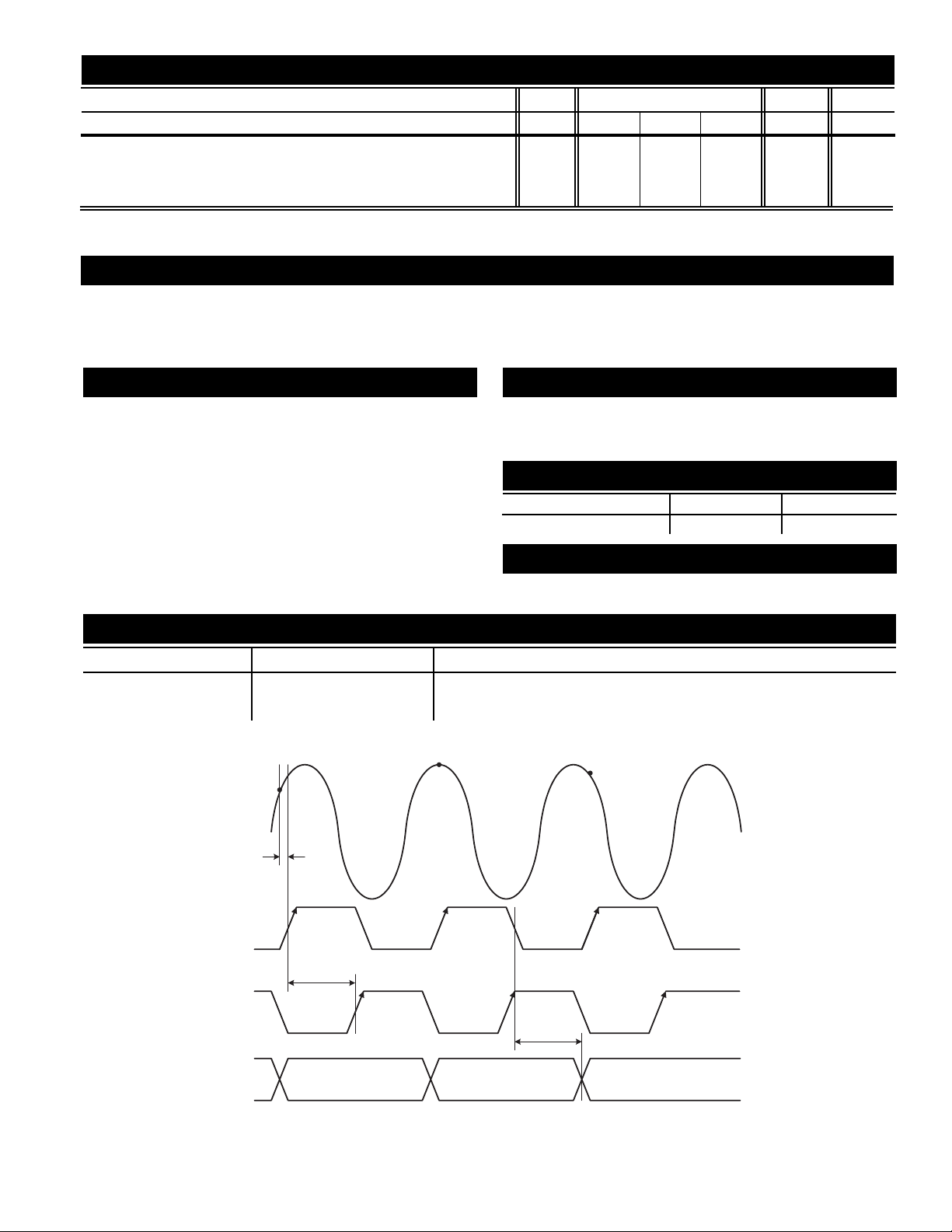
INPUT
Ta = -410ps
ENCODE
CLOCK
DAV
CLOCK
DATA
OUTPUT
N
N
Tdv = 9.6ns
N+1
N+1 N+2
Tod = 10ns
N-3 N-2 N-1
N+2
CLC5957 Timing Diagram
3
http://www.national.com
Page 4
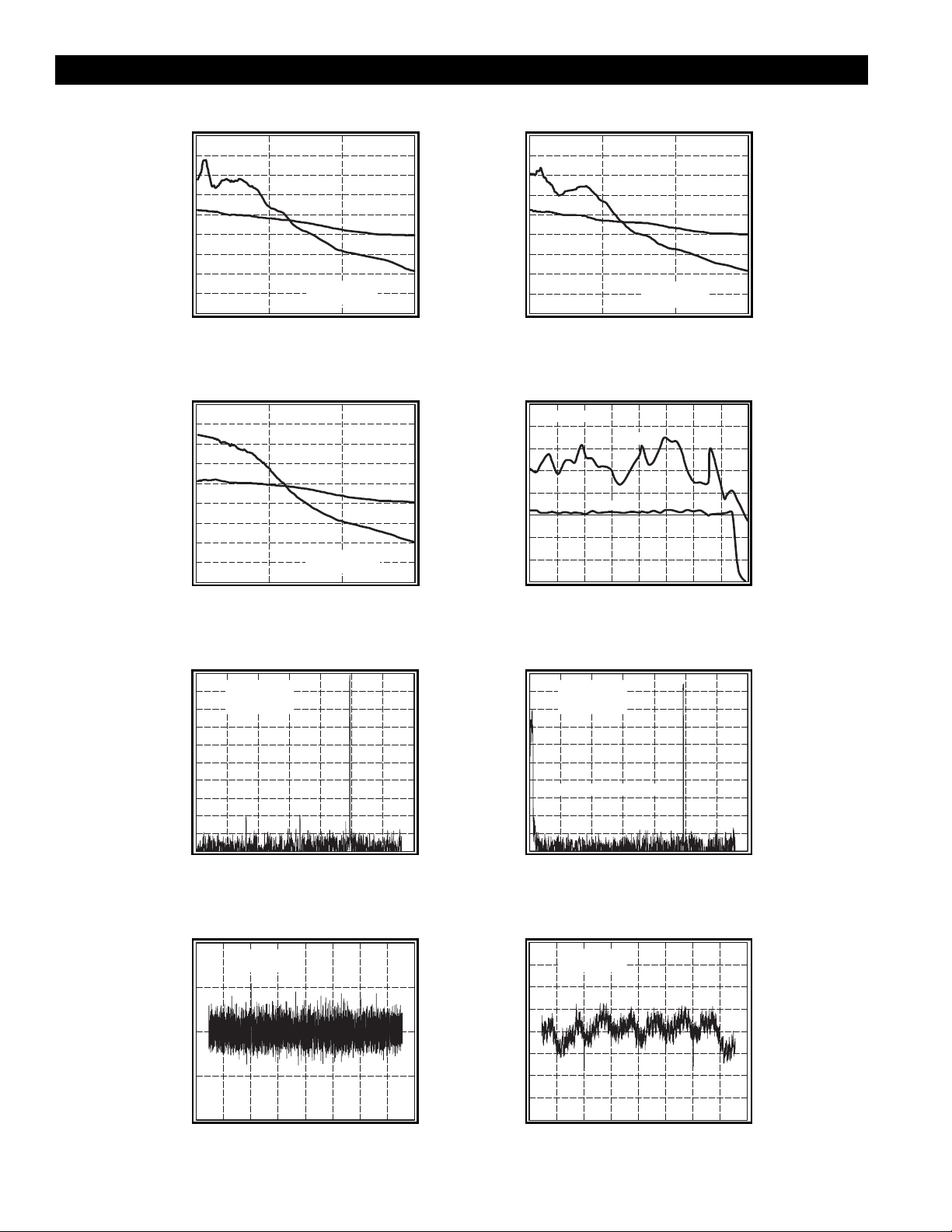
CLC5957 Typical Performance Characteristics (V
= +5V)
cc
SNR and SFDR vs. Input Frequency
85
80
75
70
65
60
SFDR
SNR
55
50
45
SNR (dBFS) and SFDR (dBc)
40
0
100
Fs = 66MSPS
A
in
Input Frequency (MHz)
SNR and SFDR vs. Input Frequency
85
80
75
70
SNR
65
SFDR
60
55
50
100
Fs = 40.96MSPS
A
in
45
SNR (dBFS) and SFDR (dBc)
40
0
Input Frequency (MHz)
= -3dBFS
200
= -3dBFS
200
300
300
SNR and SFDR vs. Input Frequency
85
80
75
70
65
SNR
SFDR
60
55
50
45
SNR (dBFS) and SFDR (dBc)
40
0
100
Fs = 52MSPS
= -3dBFS
A
in
200
Input Frequency (MHz)
SNR and SFDR vs. Sample Rate
90
Fin = 24.5MHz
85
80
SFDR
75
70
65
SNR
60
55
SNR (dBc) and SFDR (dBc)
50
40 50 60 70 80
Sample Rate (MSPS)
300
Single Tone Output Spectrum
0
-10
-20
-30
-40
-50
-60
-70
Output Level (dBFS)
-80
-90
-100
Fs = 66MSPS
= -1dBFS
A
in
F
= 24.5MHz
in
0 5 10 15 35
20
25
Frequency (MHz)
Differential Non-Linearity
1.0
0.5
0
Fs = 66MSPS
F
= 5MHz
in
DNL (LSBs)
-0.5
-1.0
0 512 1024 1536 3584
2048
2560
Output Code
3072
Single Tone Output Spectrum (w/Dither)
0
-10
-20
-30
-40
-50
-60
-70
Output Level (dBFS)
-80
-90
-100
30
Fs = 66MSPS
= - 6dBFS
A
in
F
= 24.5MHz
in
Dither Signal = 500kHz @ - 28dBFS
0 5 10 15 35
20
30
25
Frequency (MHz)
Integral Non-Linearity
4096
2.0
1.5
1.0
0.5
0
-0.5
INL (LSBs)
-1.0
-1.5
-2.0
Fs = 66MSPS
F
= 5MHz
in
0 512 1024 1536 3584
2048
2560
3072
4096
Output Code
http://www.national.com 4
Page 5

CLC5957 Typical Performance Characteristics (V
= +5V)
cc
SNR and SFDR vs.
Input Amplitude (w/o Dither)
90
80
THD
70
60
50
SFDR
40
30
20
10
SNR (dBc), SFDR (dBc), & THD (dBFS)
-50 -40 -30
SNR
Fin = 20MHz
F
-20
= 66MSPS
s
Input Amplitude (dBFS)
SNR and SFDR vs.
Input Amplitude (w/o Dither)
90
80
70
THD
60
50
SFDR
40
30
-20
Fin = 75MHz
F
= 66MSPS
s
20
10
SNR (dBc), SFDR (dBc), & THD (dBFS)
-50 -40 -30
Input Amplitude (dBFS)
-10
-10
SNR
SNR and SFDR vs.
Input Amplitude (w/Dither)
90
80
THD
70
60
50
40
SFDR
SNR
30
20
10
SNR (dBc), SFDR (dBc), & THD (dBFS)
0
-50 -40 -30 -20 -10 0
Fin = 20MHz
F
= 66MSPS
s
Input Amplitude (dBFS)
SNR and SFDR vs.
Input Amplitude (w/o Dither)
90
80
THD
70
60
50
SFDR
SNR
40
30
20
10
0
SNR (dBc), SFDR (dBc), & THD (dBFS)
-50 -40 -30
Fin = 150MHz
F
-20
= 66MSPS
s
-10
0
Input Amplitude (dBFS)
SNR and SFDR vs.
Input Amplitude (w/o Dither)
90
80
70
THD
SFDR
60
50
SNR
40
30
20
10
SNR (dBc), SFDR (dBc), & THD (dBFS)
-50 -40 -30
Fin = 250MHz
F
-20
= 66MSPS
s
Input Amplitude (dBFS)
Two Tone Output Spectrum (w/Dither)
0
-10
-20
-30
-40
-50
-60
Dither Signal =
300KHz @ -28dBFS
-70
Output Level (dBFS)
-80
-90
-100
0
51015 25
Fs
= 66MSPS
F1 = 149.5MHz
F2 = 150.5MHz
20
Frequency (MHz)
-10
Two Tone Output Spectrum (w/Dither)
0
-10
-20
-30
-40
-50
-60
-70
Output Level (dBFS)
-80
-90
-100
0
51015 25
0
Fs
= 66MSPS
F1 = 74.5MHz
F2 = 75.5MHz
Dither Signal =
300KHz @ -28dBFS
20
30
Frequency (MHz)
Two Tone Output Spectrum (w/Dither)
0
-10
-20
-30
-40
-50
-60
-70
Output Level (dBFS)
-80
-90
-100
0
30
51015 25
Fs
= 66MSPS
F1 = 249.5MHz
F2 = 251.5MHz
Dither Signal =
500KHz @ -28dBFS
20
30
Frequency (MHz)
5 http://www.national.com
Page 6

Physical Dimensions
Symbol Min Max Notes
A – 1.10
A1 0.05 0.15
A2 0.80 1.05
b 0.17 0.27
b1 0.17 0.23
c 0.09 0.20
c1 0.09 0.16
D 12.40 12.60 2
E 8.1 BSC
E1 6.00 6.20 2
e 0.50 BSC
L 0.50 0.75
L1 1.00 REF
R1 0.127
Notes:
1. All dimensions are in millimeters.
2. Dimensions D and E1 do not include mold protrusion.
Allowable protrusion is 0.20mm per side.
1GND 48 GND
2GND 47 GND
3GND 46 +DV
4GND 45 D11 (MSB)
5+AV
CC
6+AV
CC
7+AV
CC
8GND 41 D7
9ENCODE 40 D6
10ENCODE 39 D5
11GND 38 +DV
12GND 37 +DV
13A
IN
14A
IN
15GND 34 D4
16+AV
CC
17+AV
CC
18+AV
CC
19GND 30 D0 (LSB)
20GND 29 GND
21V
CM
22+AV
CC
23GND 26 GND
24GND 25 GND
CLC5957
44 D10
43 D9
42 D8
36 GND
35 GND
33 D3
32 D2
31 D1
28 OUTLEV
27 DAV
CLC5957 Pin Definitions
AIN, A
IN
CC
ENCODE,
ENCODE data conversion cycle on each rising edge.
CC
D0-D11 (Pins 30-34, 39-45) Digital data outputs are CMOS and
CC
DAV (Pin 27) Data Valid Clock. Data is valid on rising edge.
OUTLEV (Pin 28) Output Logic 3.3V or 2.5V option.
V
CM
mode voltage. This voltage is derived from an internal
GND (Pins 1-4, 8, 11, 12, 15, 19, 20, 23-26, 29, 35, 36, 47, 48)
(Pin 13, 14) Differential input with a common mode voltage
of +2.4V. The ADC full scale input is 1.024Vpp on each of
the complimentary input signals.
(Pin 9, 10) Differential clock where ENCODE
Logic for these
inputs are 50% duty cycle universal differential signal
(>200mV).
The clock input is internally biased to VCC/2 with
a termination impedance of 2.5kΩ.
TTL compatible. D0 is the LSB and D11 is the MSB. MSB
is inverted. Output coding is two’s complement.
Open = 3.3V, GND = 2.5V.
(Pin 21) Internal common mode voltage reference.
Nominally +2.4V. Can be used for the input common
bandgap reference.
circuit ground.
initiates a new
+AV
CC
+DV
CC
Bypass to ground with a 0.1µF capacitor.
http://www.national.com 6
(Pins 5-7, 16-18, 22,) +5V power supply for the analog
section. Bypass to ground with a 0.1µF capacitor.
(Pin 37, 38, 46) +5V power supply for the digital section.
Page 7

CLC5957 Applications
Analog Inputs and Bias
Figure 1 depicts the analog input and bias scheme. Each
of the differential analog inputs are internally biased to a
nominal voltage of 2.40 volts DC through a 500Ω resistor
to a low impedance buffer. This enables a simple
interface to a broadband RF transformer with a centertapped output winding that is decoupled to the analog
ground. If the application requires the inputs to be DC
coupled, the Vcm output can be used to establish the
proper common -mode input voltage for the ADC. The
Vcm voltage reference is generated from an internal
bandgap source that is very accurate and stable.
ADC
Bias Mirror
A
1.23V
Bandgap
Reference
in
A
in
500
+
500µΑ
-
–
Ω
2.4V
500
2KΩ
Ω
To T/H
and ADC
V
cm
ENCODE Clock Inputs
The CLC5957’s differential input clock scheme is
compatible with all commonly used clock sources.
Although small differential and single-ended signals are
adequate, for best aperture jitter performance a low noise
differential clock with a high slew rate is preferred. As
depicted in Figure 3, both ENCODE clock inputs are
internally biased to VCC/2 though a pair of 5KΩ resistors.
The clock input buffer operates with any common-mode
voltage between the supply and ground.
V
CCA
5kΩ 5kΩ
ENC
ENC
5kΩ 5kΩ
BJT Current Mirror
Figure 1: CLC5957 Bias Scheme
The Vcm output may also be used to power down the
ADC. When the Vcm pin is pulled above 3.5V, the inter nal
bias mirror is disabled and the total current is reduced to
less than 10mA. Figure 2 depicts how this function can
be used. The diode is necessary to prevent the logic gate
from altering the ADC bias value.
CLC5957
5V CMOS
"1" = on
"0" = off
V
ref
Figure 2: Power Shutdown Scheme
GNDA
Figure 3: CLC5957 ENCODE Clock Inputs
The internal bias resistors simplify the clock interface to
another center-tapped transformer as depicted in Figure
4. A low phase noise, RF synthesizer of moderate amplitude (1 - 4Vpp) can drive the ADC through this interface.
ENC
~
ENC
CLC5957
Figure 4: Transfer Coupled Clock Scheme
7 http://www.national.com
Page 8

Figures 5 and 6 show the clock interface schemes to
several other types of clock sources.
ENC
ENC
0.01µF
CLC5957
Figure 5: 5V CMOS Level Clock Scheme
ENC
ENC
CLC5957
0.01µF
Controlled Current
Output Buffer
V
CCD
2.4V
ref
+
Digital
Signal
10kΩ
GNDD
CML to
CMOS
+
-
50Ω
Digital
Output
Output
Level
Open = 3.3V
GND = 2.5V
Figure 7: CLC5957 Digital Outputs
The logic high level is slaved to the internal 2.4 voltage
reference. The OUTLEV control pin selects either a 3.3V
or 2.5V logic high level. An internal pullup resistor selects
the 3.3 volt level as the default when the OUTLEV pin is
left open. Grounding the OUTLEV pin selects the 2.5V
logic high level.
To ease user interface to subsequent digital circuitry, the
CLC5957 has a data valid clock output (DAV). In order to
match delays over IC processing variables, this digital
output also uses the same output buffer as the data bits.
The DAV clock output is simply a delayed version of the
ENCODE input clock. Since the ADC output data change
is slaved to the falling edge of the ENCODE clock, the
rising DAV clock edge occurs near the center of the data
valid window (or ey e) regardless of the sampling frequency.
hi
hi
Figure 6: TTL or 3V CMOS Level Clock Scheme
Digital Outputs and Level Select
Figure 7 depicts the digital output buffer and bias used in
the CLC5957. Although each of the twelve output bits
uses a controlled current buffer to limit supply transients,
it is recommended that parasitic loading of the outputs is
minimized. Because these output transients are harmonically related to the analog input signal, excessive loading
will degrade ADC performance at some frequencies.
http://www.national.com 8
Page 9

CLC5957 Evaluation Board
Description
The Evaluation board for the CLC5957 allows for easy
test and evaluation of the product. The part may be
ordered with all components loaded and tested. The
order number is the CLC5957PCASM. The user supplies
an analog input signal, encode signal and power to the
board and is able to take latched 12-bit digital data out of
the board.
ENCODE Input (ENC)
The ENCODE input is an SMA connector with a
termination of 50Ω. The encode signal is converted to an
AC coupled, differential clock signal centered between
VCC and ground. The user should supply a sinusoidal or
square wave signal of >200mVpp and <4Vpp with a 50%
duty cycle. The duty cycle can vary from 50% if the
minimum clock pulse width times are observed. A low
jitter source will be required for IF-sampled analog input
signals to maintain best performance.
CLC5957 Clock Option
The CLC5957 evaluation board is configured for use with
an optional crystal clock oscillator source. The component Y1 may be loaded with a ”Full-sized”, HCMOS type,
crystal oscillator.
Analog Input (AIN)
The analog input is an SMA connector with a 50Ω
termination. The signal is converted from single to
differential by a transformer with a 5 to 260MHz bandwidth and approximately one dB loss. Full scale is approximately 11dBm or 2.2Vpp. It is recommended that the
source for the analog input signal be low jitter, low noise
and low distortion to allow for proper test and evaluation
of the CLC5957.
Supply Voltages (J1 pins 31 A&B and 32 A&B)
The CLC5957PCASM is powered from a single 5V
supply connected from the referenced pins on the Eurocard connector. The recommended supplies are low
noise linear supplies.
Digital Outputs (J1 pins 7B (MSB, D11) through 18B
(LSB) and 20B (Data Valid))
The digital outputs are provided on the Eurocard
connector. The outputs are buffered by 5V CMOS latches
with 50Ω series output resistors. The rising edge of Data
Valid may be used to clock the output data into data
collection cards or logic analyzers. The board has a
location for the HP 01650-63203 termination adapter
for HP 16500 logic analyzers to simplify connection to
the analyzer.
9 http://www.national.com
Page 10

CLC5957 Evaluation Board Schematic
http://www.national.com 10
Page 11

CLC5957 Evaluation Board Layout
CLC5957PCASM Layer 1 CLC5957PCASM Layer 2
CLC5957PCASM Layer 3 CLC5957PCASM Layer 4
11 http://www.national.com
Page 12

CLC5957
12-bit, 70MSPS Broadband Monolithic A/D Converter
Customer Design Applications Support
National Semiconductor is committed to design excellence. For sales, literature and technical support, call the
National Semiconductor Customer Response Group at 1-800-272-9959 or fax 1-800-737-7018.
Life Support Policy
National’s products are not authorized for use as critical components in lif e support devices or systems without the e xpress written approv al
of the president of National Semiconductor Corporation. As used herein:
1. Life support devices or systems are devices or systems which, a) are intended for surgical implant into the body, or b) support or
sustain life, and whose failure to perform, when properly used in accordance with instructions for use provided in the labeling, can
be reasonably expected to result in a significant injury to the user.
2. A critical component is any component of a life support device or system whose failure to perform can be reasonably expected to
cause the failure of the life support device or system, or to affect its safety or effectiveness.
National Semiconductor National Semiconductor National Semiconductor National Semiconductor
Corporation Europe Hong Kong Ltd. Japan Ltd.
1111 West Bardin Road Fax: (+49) 0-180-530 85 86 2501 Miramar Tower Tel: 81-043-299-2309
N
Arlington, TX 76017 E-mail: europe.support.nsc.com 1-23 Kimberly Road Fax: 81-043-299-2408
Tel: 1(800) 272-9959 Deutsch Tel: (+49) 0-180-530 85 85 Tsimshatsui, Kowloon
Fax: 1(800) 737-7018 English Tel: (+49) 0-180-532 78 32 Hong Kong
Francais Tel: (+49) 0-180-532 93 58 Tel: (852) 2737-1600
Italiano Tel: (+49) 0-180-534 16 80 Fax: (852) 2736-9960
National does not assume any responsibility for use of any circuitry described, no circuit patent licenses are implied and National reserves the right at any time without notice to change said
circuitry and specifications.
http://www.national.com 12
 Loading...