

Page 1
N
CLC5902
Dual Digital T uner/AGC
0
0
May 1999
CLC5902
Dual Digital Tuner/AGC
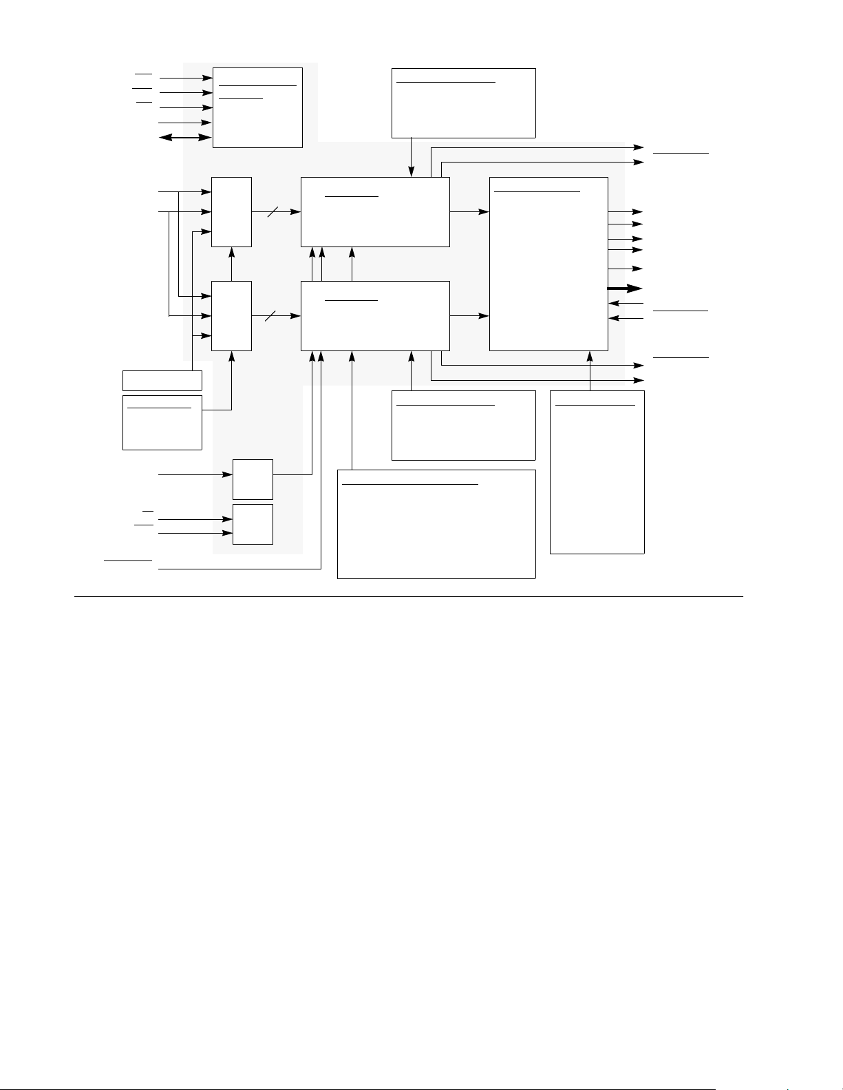
General Overview
The CLC5902 Dual Digital Tuner/AGC IC is a two channel digital
downconverter (DDC) with integrated automatic gain control
(AGC). The CLC5902 is a key component in the Diversity
Receiver Chipset (DRCS) which includes one CLC5902 Dual
Digital Tuner/AGC, two CLC5956 12-bit analog-to-digital
converters (ADCs), and two CLC5526 digitally controlled variable
gain amplifiers (DVGAs). A block diagram for a Diversity
Receiver Chipset based narrowband communications system is
shown in Figure 1. This system allows direct IF sampling of signals
up to 300MHz for enhanced receive r performance and reduced
system costs.
The CLC5902 offers high dynamic range digital tuning and
filtering based on hard-wired digital signal processing (DSP)
technology. Each channel has independent tuning, phase offset, and
gain settings. Channel filtering is performed by a series of three
filters. The first is a 4-stage Cascaded Integrator Comb (CIC) filter
with a programmable decimation ratio fr om 8 to 2048. Next there
are two symmetric FIR filters, a 21-tap and a 63-tap, both with
programmable coefficients . The first FIR filter de cimates the data
by 2, the second FIR decimates by either 2 or 4. Channel filter
bandwidth at 52MSPS ranges from ±650kHz down to ±1.3kHz.
The CLC5902’s AGC controller monitors the ADC output and
controls the ADC input signal level by adjusting the DVGA setting.
AGC threshold, deadband+hysteresis, and the loop time constant
are user defined. Total dynamic range of greater than 120dB fullscale signal to noise can be achieved with the Diversity Receiver
Chipset.
Features
n
52MSPS Operation
n
Two Independent Channels with
14-bit inputs
n
Greater than 100 dB image rejection
n
Greater than 100 dB spurious free
dynamic range
n
0.02 Hz tuning resolution
n
User Programmable AGC
n
Channel Filters include a Fourth
Order CIC follow ed by 21 -ta p and
63-tap Symmetric FIRs
n
FIR filters process 21-bit Data
with 16-bit Programmable Coefficients
n
Flexible output formats include
12-bit Floating Point or 8, 16, 24,
and 32 bit Fixed Point
n
Serial and Parallel output ports
n
JTAG Boundary Scan
n
8-bit Microprocessor Interface
n
380mW/channel, 52 MHz, 3.3V
n
128 pin PQFP package
Applications
n
Cellular Basestations
n
Satellite Receivers
n
Wireless Local Loop Receivers
n
Digital Communications
CLC5526 CLC5956 CLC5902
LC
IF A
IF B
CLK
Figure 1 Diversity Receiver Chipset Block Diagram
©1999 National Semiconductor Corporation Rev. 3.05 May 27, 1999
DVGA
DVGA
LC
ADC
ADC
12
Dual Digital
4
Tuner/AGC
12
SerialOutA/B
SerialOutB
SCK
SFS
RDY
ParallelOutput[15. .0]
ParallelOutputEnable
ParallelSelect[2..0]
Page 2
RD
WR
CE
A[7:0]
D[7:0]
Microprocessor
Interface
Channel A Controls
GAIN_A
FREQ_A
PHASE_A
AGC_IC_A
AGC_RB_A
DITH_A
AGAIN[2..0]
ASTROBE
AIN
BIN
TEST_REG
Input Source
A_SOURCE
B_SOURCE
CK
MR
AGC_EN
SI
MUX
A
MUX
B
CLK
GEN
Sync
Logic
14
14
Channel A
Tuning,
Channel Filters, and
AGC (see Figure 14)
Channel B
Tuning,
Channel Filters, and
AGC (see Figure 14)
Channel B Controls
GAIN_B
FREQ_B
PHASE_B
Common Channel Controls
DEC
DEC_BY_4
SCALE
EXP_INH
F1_COEFF
F2_COEFF
AGC_FORCE
AGC_RESET_EN
AGC_HOLD_IC
AGC_LOOP_GAIN
AGC_COUNT
AGC_TABLE
Output Formatter
Floating Point:
4-bit Exponent and
8-bit Mantissa
or
Two’s Complement:
32-bit Truncate d or
24-bit Rounded or
16-bit Rounded or
8-bit Truncated
(see Figure 26)
AGC_IC_B
AGC_RB_B
DITH_B
AOUT/BOUT
BOUT
SCK
SFS
RDY
POUT[15..0]
PSEL[2..0]
POUT_EN
BSTROBE
BGAIN[2..0]
Output Controls
RATE
SOUT_EN
SCK_POL
SFS_POL
RDY_POL
MUX_MODE
PACKED
FORMAT
DEBUG_EN
DEBUG_TAP
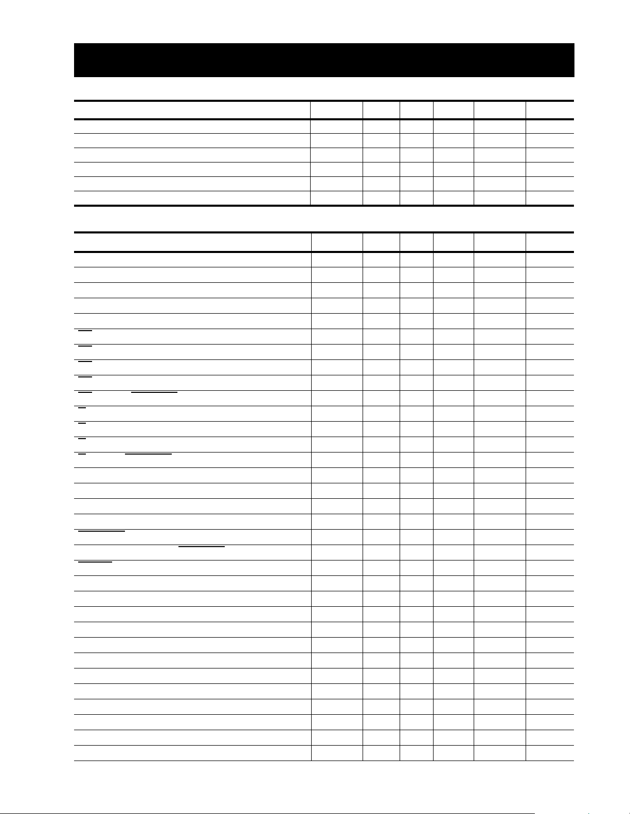
Figure 2 CLC5902 Dual Digital Tuner/AGC Block Diagram with Control Register Associations
Functional Description.
The CLC5902 block diagram is shown in Figure 2. The
CLC5902 contains two identical digital down-conversion
(DDC) circuits. Each DDC accepts a 14-bit sample at up
to 52MSPS, down converts from a selected carrier frequency to baseband, decimates the sign al rate by a programmable factor rang ing from 32 to 16384, provides
channel filteri ng, and outputs qua drature symbols.
A crossbar switch enables either of the two inputs or a test
register to be routed to either DDC ch annel. Flex ible ch annel filtering is provided by the two programma ble decimating FIR filters. The fi nal filter outputs can be
converted to a 12-bit floating point format or standard
two’s complement format. The output data is ava ilable at
both serial and parallel ports.
The CLC5902 maintains over 10 0 dB of spurious free
dynamic range and over 10 0 dB of out-of-band rejection.
This allows considerable latitude in channel filter partitioning between the analog and digital domains.
The frequencies, phase offsets, and phase dither of the two
sine/cosine numerica lly contro lled oscill ators (NCOs ) can
be independently specified. Both channels share the same
decimation ratio, bandwidth, filter coefficients, and input/
output formats.
Each channel has its own AG C circuit for use with narrowband radio channels where most of the cha nnel filtering precedes the ADC. The AGC closes the loop around
the CLC5526 DVGA, compressing the dynamic range of
the signal into the ADC . The AG C can be configure d to
operate continuously or in a gated mode. The two AGC
circuits operate independently but share the same programmed parameters and control sign als.
The chip receives configuration and control information
over a microprocessor-compatible bus consisting of an 8bit data I/O port, an 8-bit address port, a chip enable
strobe, a read strobe, and a write strobe. The chip’s control
registers (8 bits each) are memory mapped into the 8-bit
address space of the control port.
JTAG boundary scan and on-chip diagnostic circuits are
provided to simplify system debug and test.
The CLC5902 supports 3.3V I/O. The CLC5956 ADC
outputs are compatible with the CLC5902 inputs. The
CLC5902 outputs swing to the 3.3V rail so they can be
directly connected to 5V TTL inputs if desired.
Rev. 3.05 May 27, 1999 2 ©1999 National Semiconductor Corporation
Page 3
CLC5902 Electrical Characteristics
(VCC=+3.3V, 52MHz, CIC Decimation=48, F2 Decimation=2, T
DC Characteristics
PARAMETER SYMBOL MIN TYP MAX UNITS Notes
Voltage input low V
Voltage input high V
Input current I
Voltage output low (I
Voltage output high (I
Input capacitance C
AC Characteristics
= 4mA/12mA, see pin description) V
OL
= -4mA/-12mA, see pin description) V
OH
PARAMETER (CL=50pF) SYMBOL MIN TYP MAX UNITS Notes
=-40°C, T
min
IL
IH
IN
OL
OH
IN
=+85°C; unless specified)
max
-0.5 0.8 V 1
2.0 VCC+0.5 V 1
10 uA 1
0.4 V 1
2.4 V 1
4.0 pF 3
Clock (CK) Frequency (Figure 7) F
CK
52 MHz 1
Spurious Free Dynamic Range SFDR -100 dBFS
Signal to Noise Ratio SNR -127 dBFS
Tuning Resolution 0.02 Hz
Phase Resoluti on 0.005 °
MR
Active Time (Figure 5) t
MR
Inactive to first Control Port Acc ess (Fi gure 5) t
MR
Setup Time to CK (Fig ure 5) t
MR
Hold Time to CK (Figure 5) t
MR
Inactive to A|BSTROBE Release (Figure 5) t
SI
Setup Time to CK (Figure 6) t
SI
Hold Time from CK (Figure 6) t
SI
Pulse Width (Figure 6) t
SI
Inactive to A|BSTROBE Release (Figure 6) t
CK duty cycle (Figure 7) t
CK rise and fall times (V
to VIH) (Figure 7) t
IL
Input setup before CK goes high (A|BIN) (Figure 7) t
Input hold time after CK goes high (Figure 7) t
A|BSTROBE
A|BGAIN Valid Setup before A|BSTROBE
AGC_EN
Pulse Width (Figure 8) t
(Figure 8) t
Active Width (Figure 8) t
SCK to SFS Valid (Table Note A) (Figure 9) t
SCK to A|BOUT Valid (Table Note B) (Figure 9) t
RDY Pulse Width (Figure 9) t
POUT_EN Active to POUT[15..0] Valid (Figure 10) t
POUT_EN Inactiv e to POUT[15..0] Tri-State (Figure 10) t
PSEL[2..0] to POUT[ 15..0 ] Valid (Figure 11) t
RDY to POUT[15..0] New Value Valid (Table Note C) (Figure 12) t
Propagation Delay TCK to TDO (Figure 13) t
Propagation Delay TCK to Data Out (Figure 13) t
Disable Time TCK to TDO (Figure 13) t
Disable Time TCK to Data Out (Figure 13) t
Enable Time TCK to TDO (Figure 13) t
MRA
MRIC
MRSU
MRH
MRSR
SISU
SIH
SIW
SISR
CKDC
RF
SU
HD
STBPW
GSU
ENW
SFSV
OV
RDYW
OENV
OENT
SELV
RDYV
PLH
PHL
PLZ
PHZ
PZL
4 CK periods 1
10 CK periods 1
9ns1
2ns1
17 ns
9ns1
2ns1
4 CK periods 1
17 ns
40 60 % 1
3ns 1
7ns1
3ns1
1 CK period 2
1 CK period 2
2 CK periods 1
07ns1
07ns1
4 CK periods 1
15 ns 1
15 ns 1
20 ns 1
10 ns 1
30 ns 1
35 ns 1
35 ns 1
35 ns 1
035ns1
©1999 National Semiconductor Corporation 3 Rev. 3.05 May 27, 1999
Page 4
PARAMETER (C
Notes A - C
Notes 1 - 3
Absolute Maximum Ratings
Enable Time TCK to Data Out (Figure 13) t
Setup Time Data to TCK (Figure 13) t
Setup Time TDI to TCK (Figure 13) t
Setup Time TMS to TCK (Figure 13) t
Hold Time Data to TCK (Figure 13) t
Hold Time TCK to TDI (Figure 13) t
Hold Time TCK to TMS (Figure 13) t
TCK Pulse Width High (Figure 13) t
TCK Pulse Width Low (Figure 13) t
TCK Maximum Frequ ency (Figure 13) JTAG
Control Setup before the co ntrolling signal goes low (Figure 14 ) t
Control hold after the controlling signal goes high (Figure 14) t
Controlling strobe pulse wi dth (Write) (Figure 14) t
Control output delay controlling signal low to D (Read) (Figure 14) t
Control tri-state delay after controlling signal goes high (Figure 14) t
Dynamic Supply Current (F
Dynamic Supply Current (F
=52MHz, N=48) I
CK
=52MHz, N=8) I
CK
=50pF) SYMBOL MIN TYP MAX UNITS Notes
L
PZH
S
S
S
H
H
H
WH
WL
CSU
CHD
CSPW
CDLY
CZ
CC
CC
035ns1
10 ns 1
10 ns 1
15 ns 1
55 ns 1
55 ns 1
10 ns 1
55 ns 1
40 ns 1
FMAX
5ns1
5ns1
30 ns 1
230 280 mA 1
260 320 mA 1
essarily implied. Exposure to maximum ratings for extended periods may
affect device reliab i lity.
10 MHz 1
30 ns 1
20 ns 1
A. t
refers to the ri sing edge of SCK when SC K_POL=0 an d the
SFSV
falling edge when SCK_POL=1.
B. t
refers to the rising edge of SCK when SCK_POL=0 and the fall-
OV
ing edge when SCK_POL=1.
C. t
falling edge when RDY_POL=1.
1. These parameters are 100% tested at 25°C.
2. Typical specifications are the mean values of the distributions of deliverable CLC5902s tested to date.
3. Min/max ratings are based on product characterization and simulation.
Individual pa rameters a re tested as noted. Ou tgoing qu ality leve ls are
determined from tested parameters.
refers to the rising edge of RDY when RDY_POL=0 and the
RDYV
Positive Supply Voltage (VCC) -0.3V to 4.2V
Voltage on Any Input or Output Pin -0.3V to VCC+0.5V
Input Current at Any Pin ±25mA
Package Input Curre nt ±50mA
Package Dissipation a t TA=25°C 1W
ESD Susceptibility
Human Body Model
Machine Model
Soldering Temperature, Infrared, 10 seco nds 300°C
Storage Temperature -65°C to 150°C
NOTE: Absolute maximum ratings ar e limiting values, to be applie d
individually, and beyond which the serviceability of the circuit may be
impaired. Functional operability under any of these conditions is not nec-
1500V
100V
Recommended Operating Conditions
Positive Supply Voltage (VCC) 3.3V ±10%
Operating Temperature Range -40°C to +85°C
Package Thermal Resistance
Package
128 pin PQFP 39°C/W TBD°C/W
θja θjc
Reliability Information
Transistor Count 1.2 million
Ordering Information
Order Code
CLC5902VLA
CLC-DRCS-PCASM
CLC-CAPT-PCASM
Temperature
Range
-40°C to
+85°C
Description
128-pin PQFP (industrial
temperature range)
Fully loaded Diversity
Receiver Chipset eval ua tion
board and control panel software.
Data Capture board for the
DRCS with Matlab analysis
routines.
Rev. 3.05 May 27, 1999 4 ©1999 National Semiconductor Corporation
Page 5
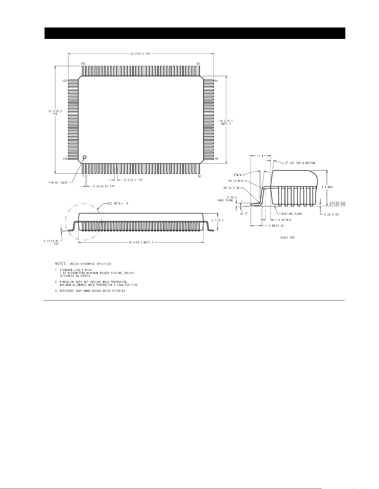
Package Dimensions
Figure 3 CLC5902 Package Dimensions
DETAIL A
Dimension are in millimeters
©1999 National Semiconductor Corporation 5 Rev. 3.05 May 27, 1999
Page 6
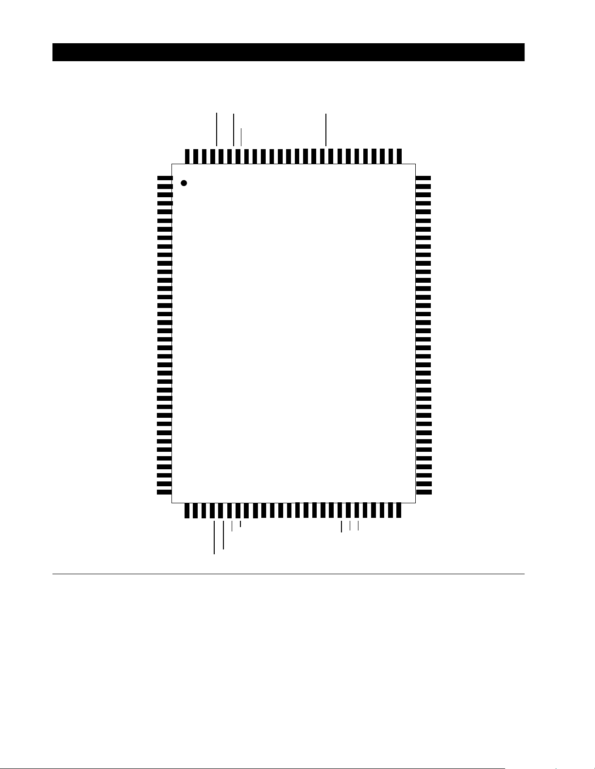
CLC5902 Pinout
AGAIN[0]
VDD
AGAIN[2]
AGAIN[1]
SCAN_EN
TRST
NC
VSS
TMS
TCK
TDI
ASTROBE
TDO
VDD
POUT_SEL[1]
VSS
POUT[1]
VDD
POUT_SEL[0]
POUT_SEL[2]
POUT_EN
POUT[0]
POUT[3]
POUT[2]
POUT[4]
VSS
NC
NC
(MSB) AIN[13]
(MSB) BIN[ 13]
VSS
AIN[12]
AIN[11]
AIN[10]
AIN[9]
AIN[8]
AIN[7]
VDD
AIN[6]
AIN[5]
AIN[4]
AIN[3]
AIN[2]
AIN[1]
AIN[0]
VSS
CK
VDD
BIN[12]
BIN[11]
BIN[10]
BIN[9]
BIN[8]
BIN[7]
VSS
BIN[6]
BIN[5]
BIN[4]
BIN[3]
BIN[2]
BIN[1]
BIN[0]
VSS
NC
1
2
3
4
5
6
7
8
9
10
11
12
13
14
15
16
17
18
19
20
21
22
23
24
25
26
27
28
29
30
31
32
33
34
35
36
37
38
127
126
128
414344
394042
125
124
123
122
121
120
119
116
118
115
114
117
113
CLC5902
Dual Digital Tuner/AGC
(Top View)
46
45
47
49
485051
535556
52
54
112
110
109
111
57
58
105
107
108
59
60
103
104
106
102
101
100
64
61
62
63
NC
NC
NC
NC
99
VSS
98
POUT[5]
97
POUT[6]
96
95
POUT[7]
POUT[8]
94
93
POUT[9]
92
VDD
POUT[10]
91
POUT[11]
90
VSS
89
88
POUT[12]
87
POUT[13]
86
POUT[14]
85
VDD
84
POUT[15]
VSS
83
AOUT
82
81
SFS
SCK
80
79
VDD
78
BOUT
77
RDY
VSS
76
D[0]
75
VDD
74
D[1]
73
72
D[2]
71
D[3]
70
D[4]
69
D[5]
68
VSS
NC
67
NC
66
NC
65
SI
VDD
BGAIN[1]
BGAIN[2]
MR
AGC_EN
BGAIN[0]
BSTROBE
VSS
A[6]
A[7]
A[5]
VSS
VDD
A[1]
A[3]
A[2]
A[4]
CE
RD
WR
A[0]
D[7]
D[6]
VSS
VDD
Figure 4 CLC5902 Pinout
Rev. 3.05 May 27, 1999 6 ©1999 National Semiconductor Corporation
Page 7
Pin Descriptions
Signal Pin DESCRIPTION
MR
AIN[13:0],
BIN[13:0]
AOUT
BOUT
(12mA drive)
AGAIN[2:0],
BGAIN[2:0]
ASTROBE
BSTROBE
SCK
(12mA drive)
SFS
(12mA drive)
POUT[15:0]
(12mA drive)
POUT_SEL[2:0] 112:114
POUT_EN
RDY
(12mA drive)
CK 20
SI
D[7:0]
(12mA drive)
,
45
4:10,12:18
22:28,30:36
82
78
125:127
40:42
124
43
80
81
84,86:88,90,91,
93:97,104:106,
108,109
111
77
46
62,63,69:73,75
MASTER RESET, Active low
Resets all registers within the chip. ASTROBE
INPUT DATA, Active high
2’s comp le ment input data. AIN[13] and BIN[13] are the MSBs. The data is clocked into the chi p on the
rising edge of the clock (CK) . Th e CLC595X connects direct ly to these input pins with no addit ion al logic.
SERIAL OUTPUT DA TA, Active high
The 2’s complement serial output data is transmitted on these pins, MSB first. The output bits change on
the rising edge of SCK (falling e dge if SCK_POL=1) and should be captu red on the falling edge of SCK
(rising if SCK_POL=1). These pins are tri-stated at power up and are enabled by the SOUT_EN control
register bit. See Figure 9 and Figure 29 timing diagrams. In Debug Mode AOUT=DE BUG[1],
BOUT=DEBUG[0].
OUTPUT DAT A TO DVGA, Active high
3 bit bus that sets the gain of the DVGA determined by the AGC circuit.
DVGA STROBE, Active low
Strobes the data into the DVGA. See Figure 8 and Figure 33 timing diagrams.
SERIAL DATA CLOCK, Active high or low
The serial data is clocke d out of the chi p by this clock. The active edg e of th e clock is user programmable.
This pin is tri-stated at power up and is enabled by the SOUT_EN control register bit. See Figure 9 and Figure 29 timing diagrams . In D ebu g Mode outputs an appropriate clo ck for the debug data.
SERIAL FRAME STROBE, Active high or low
The serial word strobe. This strobe delineates the words within the serial output streams. This strobe is a
pulse at the beginning of each serial word (PACKED=0) or each serial word I/Q pair (PACKED=1). The
polarity of this signal is use r programmable. This pin is tri -stated at power up and is enabl ed by the
SOUT_EN control register bit. See Figure 9 and Figure 29 timing diagrams. In Debug Mode
SFS=DEBUG[2].
PARALLEL OUTPUT DATA, Active high
The output data is transmitted on these pins in parallel format. The POUT_SEL[2..0] pins select one of
eight 16-bit output word s. T he P O U T_ EN
Mode POUT[15..0]=DEBUG[19..4].
PARALLEL OUTPUT DATA SELECT, Active high
The 16-bit output word is sel ecte d wi th these 3 pins according to Table 3. Not used in Debug Mode.
PARALLEL OUTPUT ENABLE. Active low
This pin enables the chip to output the selected output word on the POUT[15:0] pins. Not used in Debu g
Mode.
READY FLAG, Active high or low
The chip asserts this signal to identify the beginning of an output sample period (OSP). The polarity of this
signal is user programmable. This signal is typically used as an interrupt to a DSP chip, but can also be used
as a start pulse to dedicated circuitry. This pin is active regardless of the state of SOUT_EN. In Debug
Mode RDY=DEBUG[3].
INPUT CLOCK. Active high
The clock input to the chip. The AIN, BIN, and SI
of this clock.
SYNC IN. Active low
The sync input to the chip. The decimation counters, dither, and NCO phase can be synchronized by SI
This sync is clocked into the chi p on the rising edge of the input cloc k (CK ). Tie this pin high if external
sync is not required. All sample data is flushed by SI
BSTROBE
DATA BUS. Active high
This is the 8 bit control data I/O bus. Control register data is loade d int o the chip or read from the chip
through these pins. The chip will only drive output data on these pins when CE
is high.
are asserted during SI.
and BSTROBE are asserted during MR.
pin enables these outputs. POUT[15] is t he MSB. In Debug
input signals are clocked into the chip on the rising edge
.
. To properly initialize the DVGA ASTROBE and
is low , RD is low, and WR
Table 1 CLC5902 Pin Descriptions
©1999 National Semiconductor Corporation 7 Rev. 3.05 May 27, 1999
Page 8
Signal Pin DESCRIPTION
ADDRESS BUS. Active high
A[7:0] 48,50,52:57
RD
WR
CE
AGC_EN
TDO 116 TEST DATA OUT. Active high
TDI 117 TEST DATA IN. Active high with pull-up
TMS 118 TEST MODE SELECT. Active high with pull-up
TCK 119 TEST CLOCK. Active high
TRST
SCAN_EN
VSS
VDD
59
58
60
44
121
122
3,19,29,37,47,51,
61,68,76,83,89,
98,103,110,120
11,21,39,49,64,
74,79,85,92,107,
115,128
These pins are used to address the control registers within the chip. Each of the control registers within the
chip are assigned a unique address in a flat address space. A control register can be written to or read from
by setting A[7:0] to the register’s address.
READ ENABLE. Active low
This pin enables the chip to output the contents of the selected register on the D[7:0] pins when CE is also
low.
WRITE ENABLE. Active low
This pin enables the chip to writ e the value on the D[7:0] pins into the selected register when CE is also
low. This pin can also function as RD/WR
CHIP ENABLE. Active low
This control st ro b e enables the read or w r ite operation. Th e co ntents of the regis ter selected by A[7:0] will
be output on D[7:0] when RD
will be loaded w i th the contents of D[7:0] .
AGC ENABLE. Active low
When enabled thi s pin starts the AGC counter. The AGC will operate until the counter decrements to zero
then the AGC holds the last setting.
RESET. Active low with pull-up
Asynchronous reset for TAP controller. Tie low or to MR
SCAN ENABLE. Active low with pull-up
Enables access to interna l sc an re gisters. Tie high. Used for manufacturing test only!
Ground. Quantity 15.
Power. Quantity 12.
is low and CE is low. If WR is low and CE is low, then the selected register
if RD is held low.
if JTAG is not used.
Table 1 CLC5902 Pin Descriptions
Timing Diagrams
CK
MR
RD
or WR
A|BSTROBE
Figure 5 CLC5902 Master Reset Timing
t
MRH
t
MRA
t
MRSR
t
MRIC
t
MRSU
Rev. 3.05 May 27, 1999 8 ©1999 National Semiconductor Corporation
Page 9
CK
t
SIW
SI
A|BSTROBE
Figure 6 CLC5902 Synchronization Input (SI) Timing
1/F
CK
t
CKDC
t
CK
t
HD
t
SU
A|BIN
Figure 7 CLC5902 ADC Input and Clock Timing
CKDC
t
SIH
t
SISU
t
SISR
V
V
IL
t
RF
IH
CK
A|BSTROBE
A|BGAIN[2..0]
t
ENW
AGC_EN
Figure 8 CLC5902 DVGA Interface Timing
(n-1)
t
GSU
valid (n)
t
STBPW
©1999 National Semiconductor Corporation 9 Rev. 3.05 May 27, 1999
Page 10

SCK
SCK_POL=0
SCK
SCK_POL=1
t
SFSV
SFS
SFS_POL=0
SFS
SFS_POL=1
t
OV
A|BOUT
RDY
RDY_POL=0
RDY
t
RDYW
RDY_POL=1
Figure 9 CLC5902 Serial Port Timing
POUT_EN
t
OENV
POUT[15..0]
SCK=CK/2
t
SFSV
msb msb-1 msb-2 msb-3lsb or undef
t
OV
I Output WordPrevious Q Output Word
t
OENT
Figure 10 CLC5902 Parallel Output Enable Timing
POUT_SEL[2..0]
POUT[15..0]
t
SELV
n
output (n)
n+1
output (n+1)
Figure 11 CLC5902 Parallel Output Select Timing
RDY
RDY_POL=0
RDY
RDY_POL=1
POUT[15..0]
t
RDYV
old output
new output
Figure 12 CLC5902 Parallel Output Data Ready Timing
t
SELV
n+2
output (n+2)
Rev. 3.05 May 27, 1999 10 ©1999 National Semiconductor Corpor at ion
Page 11

TCK
t
PLH,tPHL
TDO, D
TCK
t
PZH
D
TCK
t
PZL
TDO
TCK
TMS, TDI, D
Figure 13 CLC5902 JTAG Port Timing
t
PHZ
t
PLZ
t
t
WL
t
S
1/JTAG
fmax
t
H
WH
CE
WR
RD
A[7:0]
D[7:0]
CE
WR
RD
A[7:0]
D[7:0]
CE
WR
A[7:0]
D[7:0]
CE
WR
A[7:0]
D[7:0]
t
t
t
t
CSU
CSU
CSU
CSU
t
CDLY
READ CYCLE; NORMAL MODE
t
CSPW
WRITE CYCLE; NORMAL MODE
t
CDLY
READ CYCLE; RD HELD LOW
t
CSPW
WRITE CYCLE; RD HELD LOW
t
CHD
t
CHD
t
CHD
t
CHD
t
CZ
t
CZ
Figure 14 CLC5902 Control I/O Timing
©1999 National Semiconductor Corporation 11 Rev. 3.05 May 27, 1999
Page 12

Detailed Description
()
Control Interface
The CLC5902 is configured by writing control information into 148 control registers within the chip. The contents of these control registers and how to use them are
described in Table 5. The registers are written to or read
from using the D[7:0], A[7:0], CE
, RD and WR pins (see
Table 1 for pin descriptions). This interface is designed to
allow the CLC5902 to appear to an external processor as a
memory mapped peripheral. See Figure 14 for details.
The control interface is asynchronous with respect to the
system clock, CK
. This allows the registers to be written
or read at any time. In some cases this might cause an
invalid operation since the interface is not internally synchronized. In order to assure correct operation, SI
must be
asserted after the control registers are written.
The D[7:0] , A[7:0], WR
, RD and CE pins should not be
driven above the positive supply voltage.
Master Reset
A master reset pin, MR, is provided to initialize the
CLC5902 to a known c ondition and should b e strobed
after power up. This signal will clear all sample data and
all user programmed data (filter coefficients and AGC settings). All outputs will be disabled (tri-stated). ASTROBE
and BSTROBE will be asserted to initialize the DVGA
values. Table 5 describes the control reg ister default va lues.
Synchronizing Multiple CLC5902 Chips
A system containing two or more CLC5902 chips will
need to be synchronized if coherent operation is desired.
To synchronize multiple CLC5902 chips, connect all of
the sync input pins together so they can be driven by a
common sync strobe. Synchronization occurs on the rising
edge of CK when SI
all sample data will be flus hed immediatel y, the numerically controlled oscillator (NCO) phase offset will be ini-
goes back high. When SI is asserted
tialized, the NCO dither generators will be reset, and the
CIC decimation ratio will be init ialized. O nly the con fig uration data loaded into the microprocessor interface
remains unaffected.
SI
may be held low as long as desired after a minimum of
4 CK periods.
Input Source
The input crossbar switch allows either AIN, BIN, or a
test register to be routed to the channel A or channel B
AGC/DDC. The AGC outputs, AGAIN and BGAIN, are
not switched. If AIN and BIN are exchanged the AGC
loop will be open and the AGCs will not function properly .
AIN and BIN should meet the timing requirements shown
in Figure 7.
Selecting the test register as the input source allows the
AGC or DDC operation to be verified with a known input.
See the test and diagnostics section for further discussion.
Down Converters
A detailed block diagram of each DDC chann el is shown
in Figure 15. Each down converter uses a complex NCO
and mixer to quadrature downconvert a signal to base-
band. The “FLOAT TO FIXED CONVERTER” treats the
15-bit mixer output as a mantissa and the AGC output,
EXP, as a 3-bit exponent. It performs a bit shift on the data
based on the value of EXP. This bit shifting is used to
expand the compressed dynam ic range re sulting from the
DVGA operation. The DVGA gain is adjusted in 6dB
steps which are equivalent to each digital bit shift.
The exponent (EXP) can be forced to its maximum value
by setting the EXP_INH bit. If is the DDC input,
the signal after the “FLOAT TO FIXED CONVERTER” is
x3n() xinn() ωn()cos• 2
for the I component. Changing the ‘cos’ to ‘sin’ in this
equation will provide the Q component.
xinn
•=
EXP
EQ. 1
(from AGC)
x
in
MUXA
Data @ F
= FS (F
FREQ_A
PHASE_A
EXP
n()
14
CK
SAMPLE
)
17 17
COS
SIN
NCO
EXP_INH
GAIN_A
8 TO 2K
SHIFT UP
SAT & ROUND
Data @ FCK/N Data @ FCK/N*2
N = DEC + 1
F1_COEF
21
F1 FILTER
21
DECIMATE BY 2
21
21
SAT & ROUND
DEC_BY_4
F2_COEF
I
SAT
2 OR 4
F2 FILTER
DECIMATE BY
Data @ FCK/N*2*F2_DEC
= OFS (Output F
Q
SAMPLE
TO
OUTPUT
CIRCUIT
)
CIC FILTER
DEC
DECIMATE BY
SCALE
3
EXP
EXPONENT
15
ROUND
15
22
FLOAT
TO FIXED
CONVERTER
SHIFT UP
22
x3n()
Figure 15 CLC5902 Down Converter, Channel A (Channel B is identical)
Rev. 3.05 May 27, 1999 12 ©1999 National Semiconductor Corpor at ion
Page 13

The “FLOAT TO FIXED CONVERTER” circuit expands
the dynamic range compression performed by the DVGA.
Signals from this point onward extend across the full
dynamic range of the signals applied to the DVGA input.
This allows the AGC to operate continuously through a
burst without producin g artifacts in the s ignal due to th e
settling response of the decim ation filters after a 6dB
DVGA gain adjustment. For example, if the DVGA input
signal were to increase causing the ADC output level to
cross the AGC threshold level, the gain of the DVGA
would change by -6dB. The 6dB step is allowed to propagate through the ADC and mixers and is compensated out
just before the filtering. The accuracy of the compensation
is dependent on the accuracy of the DVGA gain step. This
operating mode requ ires 21 bits (14- bit ADC output + 7bit shift) to represent the full linear dynamic range of the
signal. The output word must be set to either 24-bit or 32bit to take advantage of the entire dynamic range available. The CLC5902 can also be configured to output a
floating point format with up to 138dB of numerical resolution using only 12 output bits.
The “SHIFT UP” circuit will be discussed in the Four
Stage CIC filter section on page 14.
A 4-stage cascaded-integrator-comb (CIC) filter and a
two-stage decimate by 4 or 8 fi nite i mpulse res ponse (FIR)
filter are used to lowpass filter and isolate the desired signal. The CIC filter reduces the sample rate by a programmable factor ranging from 8 to 2048 (decimation ratio).
The CIC outputs are followed by a gain stage and then followed by a two-stage decimate by 4 or 8 filter. The gain
circuit allows the user to boost the gain of weak signals by
up to 42 dB in 6 dB steps. It also rounds the signal to 21
bits and saturates at plus or minus full scale.
The first stage of the two stage filter is a 21-tap, symmetric
decimate by 2 FIR filter (F1) with progra mmable 16 bit
tap weights. The coefficients of the first 11 taps are downloaded to the chip as 16 bit words. Since the filter is a symmetric configuration only the first 11 coefficients must be
loaded. The F1 section on page 15 provides a ge neric set
of coefficients that compensate for the rolloff of the CIC
filter and provide a passband flat to 0.01dB with 70 dB of
out of band rejection. A second coefficient set is provided
that has a narrower output passband and greater out-ofband rejection. The second set of coefficients is ideal for
systems such as GSM where far-image rejection is more
important than adjacent channel rejection.
The second stage is a 63 tap decimate by 2 or 4 program mable FIR filter (F2) also with 16 bit tap weights. Filter
coefficients for a flat response from -0.4F
to +0.4FS of
S
the output sample rate with 80dB of out of band rejection
are provided in the F2 sec tion. A second set of F2 co efficients is also provided to enhance performance for GSM
systems. The user can also design and download their own
final filter to customize the channel’s spectral response.
Typical uses of programmable filter F2 include matched
(root-raised cosine) filt ering, o r filtering to generate oversampled outputs with greater out of band rejection. The 63
tap symmetrical filter is downloaded into the chip as 32
words, 16 bits each. Saturation to plus or minus full scale
is performed at the output of F1 and F2 to clip the signal
rather than allow it to roll over.
The Numerically Controlled Oscillator
The tuning frequency of each down converter is specified
as a 32 bit word (.02Hz resolution at CK=52MHz) and the
phase offset is specified as a 16 bit word (. 005°). These
two parameters are applied to the Numerically Controlled
Complex NCO Output
0
-20
-40
-60
-80
Magnitude (dB)
-100
-120
-140
-160
-0.5 -0.4 -0.3 -0.2 -0.1 0 0.1 0.2 0.3 0.4 0.5
Frequency Normalized to F
S
(a) Befo re Phase Dithering
0
-20
-40
-60
-80
Magnitude (dB)
-100
-120
-140
-160
-0.5 -0.4 -0.3 -0.2 -0.1 0 0.1 0.2 0.3 0.4 0.5
Complex NCO Output
Frequency Normalized to F
(b) After Phase Dithering
S
Figure 16 Example of NCO spurs due to phase truncation
©1999 National Semiconductor Corporation 13 Rev. 3.05 May 27, 1999
Page 14

Oscillator (NCO) circuit to generate sine and cosine signals used by the digital mixer. The NCOs can be synchronized with NCOs on other chips via the sync pin SI
. This
allows multiple down converter outputs to be coherently
combined, each with a unique phase and amplitude.
The tuning frequency is set by loadin g the FREQ re gister
according to the formu la FREQ = 2
the desired tuning frequency and F
32
F/FCK, where F is
is the chip’s clock
CK
rate. FREQ is a 2’s complement word. The range for F is
from -F
/2 to +FCK(1-2
CK
-31
)/2.
In some cases the sampling process causes the order of the
I and Q components to be reversed. Shoul d th is occur simply invert the polarity of the tuning frequency F.
The 2’s complement format represents full-scale negative
as 10000000 and full-scale positive as 01111111 fo r an 8bit example.
The 16 bit phase offset is set by loading the PHASE register according to the formula PHASE = 2
is the desired phase in radians ranging between 0 and 2
16
P/2π, where P
π.
PHASE is an unsigned 16-bit number. P ranges from 0 to
-16
2
π(1-2
).
Phase dithering can be enabled to reduce the spurious signals created by the NCO due to p hase truncat ion. This
truncation is unavoidable sin ce the frequ ency reso lution is
much finer than the phase resolution. With dither enabled,
spurs due to phase truncation are below -100 dBc for all
frequencies and phase offsets. Each NCO has its own
dither source and the initial state of one is maximally offset with respect to the other so that they are effectively
uncorrelated. The phase dither sources are on by default.
They are independently controlled by the DITH_A and
DITH_B bits. The amplitude resolution of the ROM creates a worst-case spur amplitude of -101dBc rendering
amplitude dither unnecessary.
Complex NCO Output
Phase Dither Disabled
0
NCO frequency swept through FS/8
-20
-40
-60
-80
Magnitude (dB)
-100
-120
-140
-160
-0.5 -0.4 -0.3 -0.2 -0.1 0 0.1 0.2 0.3 0.4 0.5
Frequency Normalized to F
S
Figure 17 NCO Spurs due to Phase Quantization
Complex NCO Output
Phase Dither Enabled
0
-20
-40
-60
-80
Magnitude (dB)
-100
-120
-140
The spectrum plots in Figure 16 show the effectiveness of
phase dither in reduc ing NCO sp urs due to phas e truncation for a worst-case example (just below F
/8). With
S
-160
-0.5 -0.4 -0.3 -0.2 -0.1 0 0.1 0.2 0.3 0.4 0.5
Frequency Normalized to F
S
dither off, the spur is at -86.4dBFS. With dither on, the
spur is below -125dBFS, disappearing into the noise floor.
Figure 18 Worst Case Amplitude Spur, NCO at FS/8
This spur is spread into the noise floo r which results in an
SNR of -83.6dBFS.
Four Stage CIC Filter
Figure 17 shows the spur levels as the tuning frequency is
scanned over a narrow portion of th e freq uency rang e. The
spurs are again a result of phase quantization but their
locations move about as the frequency scan progresses. As
before, the peak spur level drops when dith ering is
enabled. When dither is enabled and the fundamental frequency is exactly at F
/8, the worst-case spur due to
S
amplitude quantization can be observed at -101dBc in Figure 18.
Rev. 3.05 May 27, 1999 14 ©1999 National Semiconductor Corpor at ion
The mixer outputs are decimated by a factor of N in a four
stage CIC filter. N is programmable to any integer
between 8 and 2048. Decimation is programmed in the
DEC register where DEC = N - 1. The programmable dec-
imation allows the chip’s usable output bandwidth to range
from about 2.6kHz to 1.3MHz when the input data rate
(which is equal to the chip’s clock rate, F
) is 52 MHz. A
CK
block diagram of the CIC filter is shown in Figure 19.
Page 15

SCALE
GAIN 2
GAIN_A
=
h1n() n, 0 … 20,,=
DATA
IN
Data @ F
= FS (F
22
CK
SAMPLE
66
SHIFT UP
)
22-bit input to SHIFT_UP is aligned
at the bottom of the 66-bit path when SCALE=0.
Figure 19 Four-stage decimate by N CIC filter
The CIC filter has a gain equal to N4 (filter decimation^4)
which must be compensated for in the “SHIFT UP” circuit
shown in Figure 19 as well as Figure 15. This circuit has a
gain equal to 2
40. This circuit divides the input signal by 2
(SCALE-44)
, where SCALE ranges from 0 to
44
providing
maximum headroom through the CIC filter. For optimal
noise performance the SCALE value is set to increase this
level until the CIC filter is just below the point of distortion. A value is normally calculated and loaded for
SCALE such that . The
GAIN
SHIFTUP
GAIN
⋅ 1≤
CIC
actual gain of the CIC filter will only be unity for powe rof-two decimation values. In other cases the gain will be
somewhat less than unity.
Channel Gain
The gain of each channel can be boosted up to 42 dB by
shifting the output of the CIC filter up by 0 to 7 bits prior
to rounding it to 21 bits. For channel A, the gain of this
stage is: , where GAIN_A ranges from 0
to 7. Overflow due to the GAIN circuit is saturated
(clipped) at plus or minus full scale. Each channel c an be
given its own GAIN setting.
First Programmable FIR Filter (F1)
The CIC/GAIN outputs are followed by two stages of filtering. The first stage is a 21 tap decimate-by-2 symm etric
FIR filter with programmable coefficients. Typically, this
filter compensates for a slight droop induced b y the CIC
filter. In addition, it often provides stopband assistance to
F2 when deep stop bands are required. The filter coefficients are 16-bit 2’s complement numbers. Unity gain will
be achieved through the filter if the sum of the 21 coeffi-
cients is equal to 2
introduce a gain equal to (sum of coefficients)/2
coefficients are identified as coefficients
The coefficients are symmetric, so only the first 11 are
loaded into the chip.
Two example sets of coefficients are provided here. The
first set of coefficients, referred to as the standard set
(STD), compensates for the droop of the CIC filter providing a passband which is flat (0.01 dB ripple) over 95% of
the final output bandwid th with 7 0dB of out- of-band rej ection (see Figure 20). Th e filter ha s a gain of 0.999 an d is
16
. If the sum is not 216, then F1 will
16
. The 21
where is the center tap.
h110()
DATA
OF N
DECIMATE
BY FACTOR
N = DEC + 1
Data @ FCK/N
OUT
symmetric with the following 11 unique taps (1|21, 2|20,
..., 10|12, 11):
29, -85, -308, -56, 1068, 1405 , -2056, -6009,
1303, 21121, 32703
Frequency Response of F1 Using STD Set
0
−10
−20
−30
−40
−50
Magnitude (dB)
−60
−70
−80
−90
−100
0 0.1 0.2 0.3 0.4 0.5
Frequency Normalized To Filter Input Sample Rate
Figure 20 F1 STD frequency response
The second set of coefficients (GSM set) are intended for
applications that need deeper stop bands or need oversampled outputs. These requirements are common in cellular
systems where out of band rejection requirements can
exceed 100dB (see Figure 21). They are useful for wideband radio architectures where the channelization is done
after the ADC. These filter coefficients introduce a gain of
0.984 and are:
-49, -340, -1008, -1617, -1269, 425, 3027, 6030,
9115, 11620, 12606
Second Programmable FIR Filter (F2)
The second stage decimate by two o r four filter also uses
externally downloaded filter coefficients. The filter coefficients are 16-bit 2’s complement numbers. Unity gain will
be achieved through the filter if the sum of the 63 coeffi-
cients is equal to 2
introduce a gain equal to (sum of coefficients)/2
The 63 coefficients are identified as
where is the center tap. The coefficients are sym-
h
31()
2
metric, so only the first 32 are loaded into the chip.
16
. If the sum is not 216, then the F2 will
16
.
h2n() n 0 … 62,,=,
©1999 National Semiconductor Corporation 15 Rev. 3.05 May 27, 1999
Page 16

Figure 21 F1 GSM frequency response
0 0.1 0.2 0.3 0.4 0.5
−120
−100
−80
−60
−40
−20
0
Frequency Response of F1 Using GSM Set
Magnitude (dB)
Frequency Normalized To Filter Input Sample Rate
Figure 22 F2 STD frequency response
0 0.1 0.2 0.3 0.4 0.5
−100
−90
−80
−70
−60
−50
−40
−30
−20
−10
0
Frequency Response of F2 Using STD Set
Magnitude (dB)
Frequency Normalized To Filter Input Sample Rate
5
0
−5
−10
−15
−20
−25
Magnitude (dB)
−30
−35
−40
−45
−50
0 0.1 0.2 0.3 0.4 0.5
Frequency Response of F2 Using GSM Set
Frequency Normalized To Filter Input Sample Rate
Figure 23 F2 GSM frequency response
An example filter (STD F2 coefficients, see Figure 22)
with 80dB out-of-band rej ection, gai n of 1.0 0, and 0.03 dB
peak to peak passband ripple is created by this set of 32
unique coefficients:
-14, -20, 19, 73, 43, -70, -82, 84, 171, -49, -269, 34, 374, 192, - 449,
-430, 460,751, -357, -1144, 81, 1581, 443, -2026,
-1337, 2437, 2886,
-2770, -6127, 2987, 20544, 29647
The filter coefficients of both filters can be used to tailor
the spectral response to the user’s needs. For example, the
first can be loaded with the standard set to provide a flat
response through to the second filter. The latter can then
be programmed as a Nyquist (typically a root-raisedcosine) filter for matched filtering of digital data.
Combined Frequency Response of CIC/F1/F2 Using STD Set
0
FCK = 52MHz
Decimation = 192
OFS = 270.83kHz
−50
Magnitude (dB)
−100
−150
0 500 1000 1500 2000 2500 3000
Frequency (KHz)
Figure 24 CIC, F1, & F2 STD frequency response
A second set of F2 co efficients (G SM set , see Figure 23)
suitable for meeting the stringent wideband GSM requirements with a gain of 0.999 are:
-536, -986, 42, 962, 869, 225, 141, 93, -280, -708,
-774, -579, -384,
-79, 536, 1056, 1152, 1067, 789, 32, -935, -1668,
-2104, -2137, -1444,
71, 2130, 4450, 6884, 9053, 10413, 10832
Rev. 3.05 May 27, 1999 16 ©1999 National Semiconductor Corpor at ion
The complete channel filter response for standard coefficients is shown in Figure 24. Pass band fl atness is sh own in
Figure 25.
The complete filter response for GSM coefficients is
shown in Figure 26.
GSM Passband flatness is shown in Figure 27.
The mask shown in Figure 26 is derived from the ET SI
GSM 5.05 specifications for a normal Basestation Transceiver (BTS). For interferers, 9dB was added to the carrier
to interference (C/I) ratios. For blockers , 9dB was added to
the difference between the blocker level an d 3dB above
the reference sensitivity level.
Page 17

Combined Frequency Response of CIC/F1/F2 Using STD Set
0.1
0.08
0.06
0.04
0.02
0
−0.02
Magnitude (dB)
−0.04
−0.06
−0.08
−0.1
0 50 100 150 200 250
Frequency (KHz)
Overall Channel Gain
The overall gain of the chip is a function of the amount of
decimation (N), the settings of the “SHIFT UP” circuit
(SCALE), the GAIN setti ng, the sum o f the F 1 coefficients, and the sum of the F2 coefficients. The overall gain
is shown below in Equation 2.
G
DDC
1
-- -
DEC 1+()
=
2
SCALE 44– AGAIN 1 EXP_INH–()⋅–[]
2
⋅
GAIN
2
⋅
GF1G
⋅⋅
F2
4
EQ. 2
Figure 25 CIC, F1, & F2 STD Passband Flatness
Combined Frequency Response of CIC/F1/F2 Using GSM Set
0
FCK = 52MHz
−20
−40
−60
Magnitude (dB)
−80
−100
0 500 1000 1500 2000 2500 3000
Frequency (KHz)
Decimation = 192
OFS = 270.83kHz
Figure 26 CIC, F1, & F2 GSM frequency response
Combined Frequency Response of CIC/F1/F2 Using GSM Set
1
0.5
0
−0.5
Magnitude (dB)
−1
Where:
21
h1i()
∑
i 1=
----------------------=
G
F1
16
2
EQ. 3
and:
63
h2i()
∑
i 1=
----------------------=
G
F2
16
2
EQ. 4
It is assumed that the DDC output words are treated as
fractional 2’s complement words. The numerators of
and equal the sums of the impulse response coeffi-
G
F2
G
F1
cients of F1 and F2, respectively. For the STD and GSM
sets, and are nearly equal to unity. Observe that
G
F1
the term in EQ. 2 is cancelled by the DVGA oper-
AGAIN
G
F2
ation so that the entire gain of the DRCS is independent of
1
the DVGA setting when EXP_INH=0. The appearing in
-- 2
EQ. 2 is the result of the 6dB conversion loss in the mixer.
1
For full-scale square wave inputs the should be set to 1
-- 2
to prevent signal distortion.
Data Latency and Group Delay
−1.5
The latency from a sync event to data output is approximately 8N CK periods for F2 decimation by 2 and 2 4N
−2
0 20 40 60 80 100
Frequency (KHz)
CK periods for F2 decimation by 4. Actual non-zero data
output can be further delayed depending on the F1 and F2
filter coefficients.
Figure 27 CIC, F1, & F2 GSM Passband Flatness
Group Delay is approximately 90N CK periods for F2
decimation by 2 or 4.
©1999 National Semiconductor Corporation 17 Rev. 3.05 May 27, 1999
Page 18

Output Modes
Note
Note
DIVIDE
BY
BOUT
AOUT
16
RATE
POUT_SEL[2..0]
POUT[15..0]
CH BCH A
SERIALIZER AND
POUT_EN
CK
SCK
3
RDY
MUX
NUMBER FORMAT
CONTROL
FORMAT
TDM FORMATTER
POLARITY INVERT
MUX_MODE
PACKED
RDY_POL, SCK_POL, SFS_POL
Figure 28 CLC5902 output circuit
SFS
SCK
After processing by the DDC, the data is then formatted
for output.
All output data is two’s complement.
Output formats include truncation to 8 or 32 bits, rounding
to 16 or 24 bits, and a 12-bit floating point format (4-bit
exponent, 8-bit mant issa, 138dB numeri c range). This
function is performed in the OUTPUT CIRCUIT shown in
Figure 28.
Serial Outputs
The CLC5902 provides a serial clock (SCK), a frame
strobe (SFS) and two data lines (AOU T and BOUT) to
output serial data. The MUX_MOD E control register
specifies whether the two c hannel o utputs are transmi tted
on two separate serial pins, or multiplex ed on to o ne pin in
a time division multiplexed (TDM) format. Separate output pins are not provided for the I and Q halves of complex data. The I and Q outputs are a lways multiplexed
onto the same serial pin. The I-compon ent is output first,
followed by the Q-component. By setting the PACKED
mode bit to ‘1’ a complex pair may be treated as a single
double-wide word. The RDY signal is used to id entify th e
first word of a complex pair of the TDM formatted output.
The TDM modes are summarized in Table 2.
The channel outputs are accessible through serial output
pins and a 16-bit parallel output port. The RDY pin is provided to notify the user that a new output sample period
(OSP) has begun. OSP refers to the interval between output samples at the decimated output rate. For example, if
the input rate (and clock rate) is 52 MHz and the overall
decimation factor is 192 (N=48, F2 decimation=2) the
OSP will be 3.69 microseconds which corresponds to an
output sample rate of 270.83kHz. An OSP starts when a
sample is ready and stops when the next one is ready.
pin.
The serial outputs power up in a tri-state
condition and must be enabled when the chip
is configured. Parallel outputs are enabled by
the POUT_EN
MUX_MODE
0 OUT
1 OUTA, OUT
SERIAL OUTPUTS
AOUT BOUT
A
B
OUT
LOW
B
Table 2 TDM Modes
The serial outputs use the format shown in Figure 29. Figure 29(a) shows the standar d output mode (the PACKED
mode bit is low). The chip clocks the frame and data out of
the chip on the rising edg e of SCK (or falling edge if the
SCK_POL bit in the input control register is set high).
Data should be captured on the falling edge of SCK (rising if SCK_POL=1). The chip sends the I data first by setting SFS high (or low if SFS_POL in the input control
register is set high) for one clock cycle, and then transmitting the data, MSB first, on as many SCK cycles as are
necessary. Without a pause, the Q data is transferred next
as shown in Figure 29(a). If the PACKED control bit is
high, then the I and Q components are sent as a double
length word with only one SFS strobe as shown in Figure
29(b). If both channels are multiplexed out the same serial
pin, then the subsequent I/Q channel words will be transmitted immediately following the first I/Q pair as shown
in Figure 29(c). Figure 29(c) also shows how the RDY
signal can be used to identify the I and Q channels in the
TDM serial transmission.The se rial output rate is programmable using the RATE register as a integer division
of the input clock , t h e di v isi on rat io ranging from 1 to 25 6.
The serial interface will not work properly if the programmed rate of SCK is insufficie nt to clo ck out al l the
bits in one OSP.
Serial Port Output Number Formats
Several numeric formats are selectable using the FORMAT control re gister. The I/Q samples can be rounded to
16 or 24 bits, or truncated to 8 bits. Th e packed mode
works as described above for these fixed point formats. A
floating point format with 138dB of dynamic range in 12
bits is also provided. The mantissa (m) is 8 bits and the
exponent (e) is 4 bits. The MSB of each segment is trans-
Rev. 3.05 May 27, 1999 18 ©1999 National Semiconductor Corpor at ion
Page 19

SCK
SFS
clock stops and data is zero after transfers are complete
AOUT
I15 I14
I1 I0 Q15 Q14
Q1 Q0
(a) UNPACKED MODE, FRAME SYNC AT THE START OF EACH WORD
clock stops and data is zero after transfers are complete
SCK
SFS
I15
AOUT
I14 I1 I0 Q15 Q14
Q1 Q0
(b) PACKED MODE, ONE FRAME SYNC AT THE START OF EACH DOUBLE-WORD TRANSFER
RDY
SFS
AOUT
SFS
AOUT
leading edge of RDY aligns with leading edge of SFS
Output Sample Period (OSP)
IA QA
IA QA IB QB IA QA IB QB
MUX_MODE=0
MUX_MODE=1
RDY is 4 CK periods wide
IA QA
(c) ONE OR TWO CHANNEL MUX MODES (PACKED MODE IS ON)
clock stops and data is zero after transfers are complete
SCK
SFS
AOUT
mI7 eI3
mI0
mI6 eI2
eI0
eQ3
(d) FLOATING POINT FORMAT
Figure 29 Serial output formats. Refer to Figure 9 for detailed timing information
mitted first. When this mode is selected, the I/Q samples
are packed regar dless of the s tate of M UX_MODE , and
the data is sent as mI/eI/eQ/mQ which allows the two
exponents to form an 8-bit word. This is shown in Figure
can be formatted as floating point numbers with an 8-bit
mantissa and a 4 bit exponent. F or t he fixed - po in t formats ,
the valid bits are justified into the MSBs of the registers of
Table 3 and all other bits are set to zero. For the floating
29(d). For all formats, once the defined length of the word
is complete, SCK stops toggling .
POUT_SEL
Normal Register
Parallel Outputs
Output data from the channels can also be taken from a
16-bit parallel port. A 3-bit word a pplied to the
POUT_SEL[2:0] pins determines which 16-bit segment is
multiplexed to the parallel port. Table 3 defines this mapping. To allow for bussing of multiple chips, the parallel
port is tri-stated unless POUT_EN
is low. The RDY sig-
nal indicates the start of an OSP and that new data is ready
at the parallel output. The user has one OSP to cycle
through whichever registers are needed. The RAT E register must be set so that each OSP is at least 5 SCK periods.
0 IA upper 16 bits 0000/eIA/mIA
1 IA lower 16 bits 0 x0000
2 QA upper 16 bits 0000/eQA/mQA
3 QA lower 16 bits 0x0000
4 IB upper 16 bits 0000/eIB/mIB
5 IB lower 16 bits 0x0000
6 QB upper 16 bits 0000/eQ B/ mQB
7 QB lower 16 bits 0x0000
Table 3 Register Selection for Parallel Output
Parallel Port Output Numeric Formats
The I/Q samples can be rounded to 16 or 24 bits or the full
32 bit word can be read. By setting the word size to 32 bits
it is possible to read out the top 16 bits and only observe
the top 8 bits if desired. Additionally, the output samples
point format, the valid bits are placed in the upper 16 bits
of the appropriate channel register using the format 0000/
eI/mI for the I samples.
eQ0 mQ0
mQ7
Contents
Register Contents
Floating Point
©1999 National Semiconductor Corporation 19 Rev. 3.05 May 27, 1999
Page 20

AGC
Figure 30 Output Gain Scaling vs. Input Signal
Input Power
ADC Output
ADC Full Scale
AGC Threshold
Deadband+Hysteresis
Output Power
D
D
C
O
u
t
p
u
t
Diversity Receiver
A
G
C
O
perates
O
ver T
h
i
s
R
an
g
e
Chipset Full Scale
Figure 31 AGC Setup.
DVGA Input Power
DVGA Output Power
Deadband
Hysteresis=Deadband-6dB
Reference
6dB
6dB
Setpoint
The CLC5902 AGC proces so r monitors the out put l evel of
the ADC and servos it to the desired setpoint. The ADC
input is controlled by the DVGA to maintain the proper
setpoint level. DVGA operation results in a compression
of the signal through the ADC. The DVGA signal com pression is reversed in the CLC5902 to provide > 120dB
of linear dynamic range. This is illustrated in Figure 30.
6dB steps the deadband should always be g reater than 6d B
to prevent oscillation. An increased deadband value will
reduce the amount of AGC operation. A decreased deadband value will increase the amount of AGC operation but
will hold the ADC output closer to the setpoint. The
threshold should be set so th at transien ts do no t cause sustained overrange at the ADC inputs. The thres hold setting
can also be used to set the ADC input near its optimal performance level.
The AGC may be configured to free run, o perate for a pro grammable period of ti me ( burst mode), or sto p r unn in g.
a burst start pulse is applied to the AGC_EN
pin in burst
mode, the AGC will free run for AGC_HOLD_COUNT
CK periods then freeze. At the beginning of the next burst
either the freeze value is maintained or an initial condition
is set from AGC_IC_A|B based on
AGC_RESET_EN.
Allowing the AGC to free run should be appropriate for
most applications. Table 4 shows the AGC mode control
bits.
AGC Mode AgcHldIC AgcRstEn AgcForce
Free Run 0 0 1
Burst, hold previous value 0 0 0
Burst, use initial conditions 0 1 0
Manual 100
If
In order to use the AGC the DRCS Control Panel software
should be used to calculate the programmable parameters.
To generate these parameters only the desired setpoint,
deadband+hysteresis, and loop time constant need to be
supplied. All subsequent cal cul ati on s ar e perf orm ed by t he
software. Complete details of the AGC operation are provided in an appendix but are not required reading.
AGC setpoint and deadband+hysteresis are illustrated in
Figure 31. The loop time constant is a measure of how fast
the loop will track a changing signal. Values down to
approximately 1.0 microsecond will be stable with the second order LC noise filter. Since the DVGA operates with
Rev. 3.05 May 27, 1999 20 ©1999 National Semiconductor Corpor at ion
Table 4 AGC Operating Modes
Power Management
The CLC5902 can be placed in a low power (static) state
by stopping the input clock. To prevent this from placing
the CLC5902 into une xpected state s, the SI
CLC5902 should be asserted prior to disabling the input
clock and held asserted until the inp ut cloc k has return ed
to a stable condition.
pin of the
Page 21

Test and Diagnostics
The CLC5902 supports IEEE 1149.1 compliant JTAG
Boundary Scan for the I/O’s. The following pins are used:
TRST (test reset)
TMS (test mode select)
TDI (test data in)
TDO (test data out)
TCK (test clock)
The following JTAG instructions are supported:
Instruction Description
BYPASS Connects TDI directly to TDO
EXTEST Drives the ‘extest’ TAP controller output
IDCODE Connects the 32-bit ID register to TDO
SAMPLE/PRELOAD Drives the ‘samp_load’ TAP controller output
HIGHZ Tri-states the outputs
The JTAG Boundary Scan can be used to verify printed
circuit board continuity at the system level.
The user is able to program a value into TEST_REG and
substitute this for the normal channel inputs from the AIN/
BIN pins by selecting it with the crossbar. With the NCO
frequency set to zero this allows the DDCs and the output
interface of the chip to be verified. Also, the AGC loop
can be opened by setting AGC_HOLD_IC high and setting the gain of the DVGA by programming the appropriate value into the AGC_IC_A/B register.
Real-time access to the followin g signals is provided by
configuring the control interface debug register:
• NCO sine and cosine outputs
• data after round following mixers
• data befo r e F1 and F2
• data after the CIC filter within the AGC
The access points are mul tiplexe d to a 20-bi t paralle l output port which is created from signal pins POUT[15:0],
AOUT, BOUT, SFS, and RDY according to the table
below:
Normal Mode Pin
POUT[15:0] DEBUG[19..4]
RDY DEBUG[3]
SFS DEBUG[2]
AOUT DEBUG[1]
BOUT DEBUG[0]
SCK will be set
tap point. POUT_EN
Debug Mode Pin
to the proper strobe rate for each debug
and PSEL[2..0] hav e no effect in
Debug Mode. The outputs are tur ned on w hen the Debug
Mode bit is set. Normal serial outputs are also disabled.
Control Registers
The chip is configured and controlled through the use of 8bit control registers. These registers are accessed
ing or writing using the control bu s pins (CE
A[7:0], and D[7:0]) described in the Control Interface section. The register names and descriptions are listed in
T a ble 5.
for read-
, RD, WR,
Control Registers
Register Name Width Type DefaultaAddr Bit Description
DEC 11b R/W 7 0(LSBs)
DEC_BY_4 1b R/W 0 1 4 Controls the decimation factor in F2. 0=Decimate by 2. 1=Decimate by 4. This affects both
SCALE 6b R/W 0 2 5:0 CIC SCALE parameter. Format is an unsigned integer representing the number of left bit
GAIN_A 3b R/W 0 3 2:0 Value of left bit shift prior to F1 for channel A.
GAIN_B 3b R/W 0 4 2:0 Value of left bit shift prior to F1 for channel B.
RATE 1B R/W 1 5 7:0 Determines rate of serial output clock. The output rate is FCK/(RATE+1). Unsigned integer.
SOUT_EN 1b R/W 0 6 0 Enables the serial output pins AOUT, BOUT, SCK, and SFS. 0=Tristate. 1=Enabled.
SCK_POL 1b R/W 0 6 1 Determines polarity of the SCK output. 0=AOUT, BOUT, and SFS change on the ri sing edge
SFS_POL 1b R/W 0 6 2 Determines polarity of the SFS output. 0=Active High. 1=Active Low.
RDY_POL 1b R/W 0 6 3 Determines polarity of the RDY output. 0=Active High. 1=Active Low.
MUX_MODE 1b R/W 0 6 4 Determines the mode of the serial outputs. 0=Each channel is output on its respective pin,
PACKED 1b R/W 0 6 5 Controls when SFS goes active. 0=SFS pulses prior to the start of the I and the Q words.
FORMAT 2b R/W 0 6 6:7 Determines output number format. 0=Truncate serial output to 8 bits. Parallel output is trun-
1(MSBs)
Table 5 CLC5902 Control Registers
7:0
2:0
CIC decimation control. N=DEC+1. Valid range is from 7 to 2047. Format is an unsigned
integer. This affects both channels.
channels.
shifts to perform on the data prior to the CIC filter. Valid range is from 0 to 40. This affects
both channels.
of SCK (capture on falling edge). 1=They change on the falling edge of SCK.
1=Both channels are multiplexed and output on AOUT. See also Table 2.
1=SFS pulses only once prior to the start of each I/Q samp l e p air ( i.e. the pa ir is tre ated a s a
double-sized word) The I word precedes the Q word. See Figure 29.
cated to 32 bits. 1=Round both serial and parallel to 16 bits. All other bits are set to 0.
2=Round both serial and parallel to 24 bits. A ll other bit s are set to 0. 3=Output fl oating point.
8-bit mantissa, 4-bit exponent. All other bits are set to 0.
©1999 National Semiconductor Corporation 21 Rev. 3.05 May 27, 1999
Page 22

Register Name Width Type DefaultaAddr Bit Description
FREQ_A 4B R/W 0 7-10 7:0 Frequency word for channel A. Format is a 32-bit, 2’s complement number spread across 4
PHASE_A 2B R/W 0 11-12 7:0 Phase word for channel A. Format is a 16-bit, unsigned magnitude number spread across 2
FREQ_B 4B R/W 0 13-16 7:0 Frequency word for channel B. Format is a 32-bit, 2’s complement number spread across 4
PHASE_B 2B R/W 0 17-18 7:0 Phase word for channel B. Format is a 16-bit, unsigned magnitude number spread across 2
A_SOURCE 2 R/W 0 19 1:0 0=Select AIN as channel input source. 1=Select BIN. 2=3=Select TEST_REG as channel
B_SOURCE 2 R/W 1 19 2:3 0=Select AIN as channel input source. 1=Select BIN. 2=3=Select TEST_REG as channel
EXP_INH 1b R/W 0 20 0 0=Allow exponent to pass into FLOAT TO FIXED converter . 1 =For ce expon ent in DDC chan -
AGC_FORCE 1b R/W 1 20 1 0=Enable AGC counter operation. 1=AGC loop operates continuously regardless of
AGC_RESET_EN 1b R/W 0 20 2 0=Initial condition is never used. 1=Integrator is reset each time the AGC transitions from
AGC_HOLD_IC 1b R/W 0 20 3 0=Normal closed-loop operation. 1=Hold integrator at initial condition. This affects both
AGC_LOOP_GAIN 2b R/W 0 20 4:5 Bit shift value for AGC loop. Valid range is from 0 to 3. This affects both channels.
AGC_COUNT 2B R/W 0 21-22 7:0 Counter value for AGC enable counter. Format is a 16-bit, unsigned magnitude number
AGC_IC_A 1B R/W 0 23 7:0 AGC integrator initial condition for channel A. Format is an 8-bit, unsigned magnitude num-
AGC_IC_B 1B R/W 0 24 7:0 AGC integrator initial condition for channel B. Format is an 8-bit, unsigned magnitude num-
AGC_RB_A 1B R 0 25 7:0 AGC integrator readback value for channel A. Format is an 8-bit, unsigned magnitude num-
AGC_RB_B 1B R 0 26 7:0 AGC integrator readback value for channel B. Format is an 8-bit, unsigned magnitude num-
TEST_REG 14b R/W 0 27(LSBs)
Reserved 1B - - 29 7:0 For future use.
Reserved 1B - - 30 7:0 For future use.
DEBUG_EN 1b R/W 0 31 0 0=Normal. 1=Enables access to the internal probe points.
DEBUG_TAP 5b R/W 0 31 1:5 Selects internal node tap for debug.
DITH_A 1b R/W 1 31 6 0=Disable NCO dither source for channel A. 1=Enable.
DITH_B 1b R/W 1 31 7 0=Disable NCO dither source for channel B. 1=Enable.
AGC_TABLE 32B R/W 0 128-159 7:0 RAM space that defines key AGC loop parameters. Format is 32 separate 8-bit, 2’s comple-
F1_COEFF 22B R/W 0 160-181 7:0 Coefficients for F1. Format is 11 separate 16-bit, 2’s complement numbers, ea ch on e sp read
F2_COEFF 64B R/W 0 182-245 7:0 Coefficients for F2. Format is 32 separate 16-bit, 2’ s comple ment number s, each one spread
28(MSBs)
7:0
5:0
registers. The LSBs are in the lower registers. The NCO frequency F is F/FCK=FREQ_A/232.
registers. The LSBs are in the lower registers. The NCO phase PHI is PHI=2*pi*PHASE_A/
2^16.
registers. The LSBs are in the lower registers. The NCO frequency F is F/FCK=FREQ_B/232.
registers. The LSBs are in the lower registers. The NCO phase PHI is PHI=2*pi*PHASE_B/
2^16.
input source.
input source.
nel to a 7 (maximum digital gain). This affects both channels.
AGC_EN pin. This affects both channels.
idle to active. This affects both channels.
channels.
spread across 2 registers. The LS Bs a re in the low e r re gister. The value represents the number of CK cycles over which the loop is active.
ber. This number is written into the magnitude MSBs of the channel A AGC integrator whenever it is reset to the initial condition.
ber. This number is written into the magnitude MSBs of the channel B AGC integrator whenever it is reset to the initial condition.
ber. The user can read the magnitude MSBs of the channel A integrator from this register.
ber. The user can read the magnitude MSBs of the channel B integrator from this register.
Test input source. Instead of processing values from the AIN/BIN pins, the value from this
location is used instead. Format is 14-bit 2s complement number spread across 2 registers.
0 selects F1 output for BI, 20 bits
1 selects F1 output for BQ, 20 bits
2 selects F1 output for AQ, 20 bits
3 selects F1 output for AI, 20 bits
4 selects F1 input for BI, 20 bits
5 selects F1 input for BQ, 20 bits
6 selects F1 input for AI, 20 bits
7 selects F1 input for AQ, 20 bits
8 selects NCO A, cosine output. 17 bits, 3 LSBs are 0.
9 selects NCO A, sine output, 17 bits, 3 LSBs are 0.
10 selects NCO B, cosine output, 17 bits, 3 LSBs are 0.
11 selects NCO B, sine output, 17 bits, 3 LSBs are 0.
12 selects NCO AI, rounded output, 15 bits, 5 LSBs are 0.
13 selects NCO AQ, rounded output, 15 bits, 5 LSBs are 0.
14 selects NCO BI, rounded output, 15 bits, 5 LSBs are 0.
15 selects NCO BQ, rounded output, 15 bits, 5 LSBs are 0.
16-31 selects AGC CIC filter output. 9 MSBs from ch A, next 9 bits from ch B, 2 LSBs are 0.
ment numbers. This is common to both channels.
across 2 registers. The LSBs are in the lower regi sters. For exam pl e, coef ficien t h0[7:0 ] is in
address 160, h0[15:8] is in address 161, h1[7:0] is in address 162, h1[15:8] is in address
163.
across 2 registers. The LSBs are in the lower regi sters. For exam pl e, coef ficien t h0[7:0 ] is in
address 182, h0[15:8] is in address 183, h1[7:0] is in address 184, h1[15:8] is in address
185.
Table 5 CLC5902 Control Registers
a. These are the default values set by a master reset (MR). Sync in (SI) will not affect any of the s e values.
Rev. 3.05 May 27, 1999 22 ©1999 National Semiconductor Corpor at ion
Page 23

Condensed Hexadecimal Address Map
Bit4
Dec4
y
Scale4
Rate4
FA4
FA12
FA20
FA28
PA4
PA12
FB4
FB12
FB20
FB28
PB4
PB12
g
g
g
g
g
g
g
Test4
Test12
g
g
The FIR C oefficients loa d from the low address to the high address in this order
y
Reg Name Addr Bit7 Bit6 Bit5
DEC
DEC_BY_4
SCALE
GAIN1_A
GAIN1_B
RATE
SERIAL_CTRL
FREQ _A
PHASE_A
FREQ _B
PHASE_B
SOURCE
AGC_CTRL
AGC_COUNT
AGC_IC_A
AGC_IC_B
AGC_RB_A
AGC_RB_A
TEST_REG
DEBUG
AGC_TABLE
F1_COEFF
F2_COEFF
[
[
[
[
[
[
[
[
[
[
[$
[%
[&
['
[(
[)
[
[
[
[
[
[
[
[
[
[
[$
[%
[&
[)
[
[)
[$
[%
[%
[)
Dec7 Dec6 Dec5
Scale5
Rate7 Rate6 R ate5
FMT1 FM T0 Packed MuxMode RDY_POL SFS_POL SCK_POL SOUT_EN
FA7 FA6 FA5
FA15 FA14 FA13
FA23 FA22 FA21
FA31 FA30 FA29
PA7 PA6 PA5
PA15 PA14 PA13
FB7 FB6 FB5
FB15 FB14 FB13
FB23 FB22 FB21
FB31 FB30 FB29
PB7 PB6 PB5
PB15 PB14 PB13
cCn t7 AgcCn t6 AgcCnt5 AgcCnt4 AgcCnt3 AgcCnt2 AgcCnt1 AgcCnt0
A
A
cCnt15 AgcCn t1 4 AgcCnt13 AgcCnt12 AgcCnt11 AgcCnt10 AgcCnt9 AgcCnt8
cIcA7 AgcIcA6 AgcIcA5 AgcIcA4 AgcIcA3 AgcIcA2 AgcIcA1 AgcIcA0
A
cIcB7 AgcIcB6 AgcIcB5 AgcIcB4 AgcIcB3 AgcIcB2 AgcIcB1 AgcIcB0
A
cRb A7 AgcRb A6 AgcRbA5 AgcRbA 4 AgcRbA 3 AgcRbA 2 AgcRbA 1 AgcRbA 0
A
cRb B7 AgcRb B6 AgcRbB5 AgcRbB 4 AgcRbB 3 AgcRbB 2 AgcRbB 1 AgcRbB 0
A
Test7 Test6 Test5
DITH_ B D IT H_A T apSel4 TapSe l3 T apSel2 Tap Sel1 TapSel0 D ebu
The A
1st location, 2nd location…
1st location low b
A
Test13
c Table loads from the low address to the high address in this order:
Bit3 Bit2 Bit1 Bit0
Dec3 Dec2 Dec1 Dec0
4 Dec10 Dec9 Dec8
DecB
cLG1 AgcLG0 AgcHldIC AgcRstEn AgcForce ExpInh
te, 1 s t loc a tio n h igh byte, 2nd location…
Scale3 Scale2 Scale1 S cale0
G1A2 G1A1 G1A0
G1B2 G1B1 G1B0
Rate3 Rate2 Rate1 R ate0
FA3 FA2 FA1 FA0
FA11 FA10 FA9 FA8
FA19 FA18 FA17 FA16
FA27 FA26 FA25 FA24
PA3 PA2 PA1 PA0
PA11 PA10 PA9 PA8
FB3 FB2 FB1 FB0
FB11 FB10 FB9 FB8
FB19 FB18 FB17 FB16
FB27 FB26 FB25 FB24
PB3 PB2 PB1 PB0
PB11 PB10 PB9 PB8
BSrc1 BSrc0 ASrc1 ASrc0
Test3 Test2 Test1 Test0
Test11 Test10 Test9 Test8
En
©1999 National Semiconductor Corporation 23 Rev. 3.05 May 27, 1999
Page 24

A block diagram of the AGC is shown in Figure 32. The
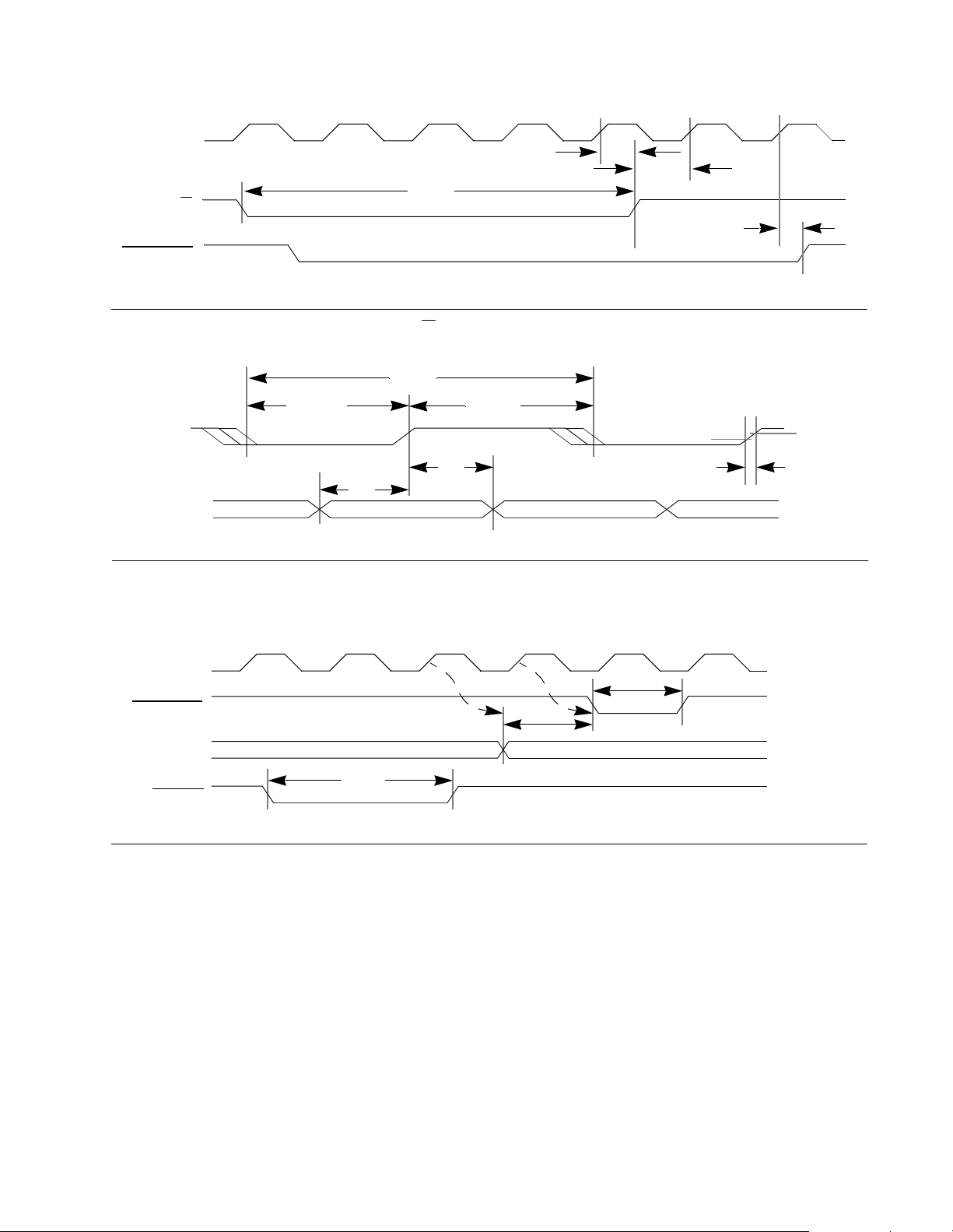
AGC Theory of Operation
DVGA interface comprises four pins for each of the channels. The first three pins of this interface are a 3-bit binary
word that controls the
The final pin is ASTROBE
to be
latched into the DVGA’s register. A key feature of
the ASTROBE
only if the data on AGAIN
cycle. Not shown is that ASTROBE
independent. For example, ASTROBE
when AGAIN has changed. BSTROBE
DVGA gain in 6dB steps (AGAIN).
which allows the AGAIN bits
, illustrated Figu re 33, is th at it toggl es
has changed from the previous
and BSTROBE are
should only toggle
should not toggle
because AGAIN has changed. This is done to minimize
unnecessary digital noise on
through the DVGA. ASTROBE
asserted during MR
and SI to properly initialize the
the sensitive analog path
and BSTROBE are
DVGAs.
The absolute value circuit and the 2-stage, decimate-by-8
CIC filter comprise the power detection part of the AGC.
The power detector bandwidth is set by the CIC filter to
F
/8. The absolute value circuit doubles th e effective
CK
input frequency. This has the effect of reducing the power
detector b andwidth fro m F
/8 to FCK/16.
CK
For a full-scale sinusoidal input, the absol ute value circuit
output is a dc value of . Because the absolut e
511 2 π⁄()⋅
value circuit also generates undesired even harmonic
terms, the CIC filter (response shown in Figure 34), is
required to remove these harmonics. The first response
null occurs at F
/8, where FCK is the clock frequency,
CK
and the response magnitude is at least 25dB below the dc
value from F
/10 to 9FCK/10. Because the 2nd harmonic
CK
from the absolute value circuit is about 10 dB below the dc
this means that the ripple in the detected level is about
0.7dB or less for input freque ncies between F
19F
/20.
CK
CK
The “FIXED TO FLOAT CONVERTER” takes the fixed
point 9-bit output from the CIC filter and converts it to a
“floating point” number. This conversion is done so that
the 32 values in the RAM ca n be unifo rmly assigned (dB
AGC_TABLE
AGC_LOOP_GAIN
EXP
/20 to
AIN[13:4]
AGC_COUNT
AGC_EN
10
VALUE
ABSOLUTE
16
SHIFT DOWN
AGC_FORCE
PERIOD
LOAD
EN
COUNTER
2 STAGE
CIC FILTER
DECIMATE BY 8
16
Figure 32 CLC5902 AGC circuit, Channel A
1 SCK delay
CK
CK/8
P
OUT
9
AGC_HOLD_IC
12
5
FIXED
TO FLOAT
CONVERTER
8
RAM
32X8
SHIFT DOWN
AGC_RESET_EN
ONE SHOT
ASTROBE does not pulse because AGAIN[2:0] does not change
12
MUX
FUNCTION PROGRAMMED
LOG
3
AGC_IC_A
INTO RAM
-REF
AGAIN
ASTROBE
AGAIN[2:0]
Figure 33 Timing diagram for AGC/DVGA interface, Channel A. Refer to Figure 8 for detailed timing information.
Rev. 3.05 May 27, 1999 24 ©1999 National Semiconductor Corpor at ion
Page 25

0
-10
-20
-30
Magnitude (dB)
-40
-50
-60
0 0.1 0.2 0.3 0.4 0.5 0.6 0.7 0.8 0.9 1
Frequency Normalized to Sample Rate
As shown in Figure 32, the 32X8 RAM look-up table
implements the functions of log converter, reference subtraction, error amplifier, and deadba nd. The user must
build each of these functions by constructing a set of 8-bit,
2’s complement nu mbers to be loaded into the RAM. Each
of these functions and how to construct them are discussed
in the following paragraphs .
A log conversion is done in order to keep the loop gain
independent of operating point. To see why this is beneficial, the control gain of the DVGA computed without log
conversion is,
GG
K
′
DVGA
∂
v
G∂
v
i
2
⋅(),=
i
–()
2()2
o
GGo–()
,⋅ln⋅–=
EQ. 6
Figure 34 Power detector filter response
scale) to detected power levels (54 db range). This provides a resolution of 1.7d B between detect ed power levels.
The truth table for this converter is given in Table 6. The
upper three bits of the output represent the exponent (e)
INPUT
0-3 000XX
4-7 001XX
8-15 010XX
16-31 011XX
32-63 100XX
64-127 101XX
128-255 110XX
256-511 111XX
OUTPUT
(eeemm)
Table 6 Fixed to Float Converter Truth Table
and the lower 2 are the mantissa (m). The exponent is
determined by the position of the leading ‘1’ out of the
CIC filter. An output of ‘001XX’ corresponds to a leading
‘1’ in bit 2 (LSB is bit 0). The exponent increases by one
each time the leading ‘1’ advances in bit position. The
mantissa bits are the two bits that follow the leading ‘1’. If
we define E as the decimal value of the exponent bits and
M as the decimal value of the mantissa bits, the output of
the CIC filter, P
, corresponding to a given “FIXED TO
OUT
FLOAT CONVERTER” output is,
P
OUT
4 min E 1,()⋅ M+[]
max E 1,()1–()
2
⋅=
EQ. 5
E 1.≥,
The max() and min() operators account for row 1 of Table
6 which is a special case because M=P
. Equation 5
OUT
associates each address of the RAM with a CIC filter output.
where G is the decimal equivalent of GAIN and G
accounts for the DVGA gain in excess of unity. This equa-
tion assumes that the DVGA gain control polarity is positive as is the case for the CLC5526. The gain around the
entire loop must be negative. Observe in Equation 6 that
the control gain is dependent on operating poin t G. If we
instead compute the control gain with log conversion,
K
DVGA
∂
20 v
G∂
GGo–()
2
⋅()log⋅[],=
i
EQ. 7
6.02,–=
which is no longer operating-point dependent. The log
function is constructed by com puting the CIC filter outpu t
associated with each address (Equation 5) and c onverting
these to dB. Full scale (dc signal) is .
20 511()54dB=log
The reference subtraction is constructed by subtracting the
desired loop servo point (in dB) from the table v alues
computed in the previous paragraph . For example, if it is
desired that the DVGA servo the ADC input level (sinusoidal signal) to -6dBFS, the number to subtract from the
data is
2
511
-- -
-------- -
20
⋅
π
2
.
44dB=log
EQ. 8
The table data will then cross through zero at the address
corresponding to this reference level. A deadband wider
than 6dB should then be constructed symmetrically about
this point. This prevents the loop from hunting due to the
6dB gain steps of the DVGA. Any deadband in e xcess of
6dB appears as hysteresis in the servo point of the loop as
illustrated in Figure 31. The deadband is constructed by
loading zeros into those addresses on either side of the one
which corresponds to the reference level.
The last function of the RAM table is that of error amplification. All the operations preceding this one gave a table
slope . This must now be adjusted in order to
S
RAM
1=
control the time constant of the loop given by,
o
©1999 National Semiconductor Corporation 25 Rev. 3.05 May 27, 1999
Page 26

τ
8
F
CK
----------
1
G
L
------ -
1
2
-- -+
.=
20
20
0
-20
-40
-60
-80
AGC RAM CONTENTS
-100
-120
0 5 10 15 20 25 30
ADDRESS
(a)
Figure 35 Example of programmed RAM contents
EQ. 9
The term GL in this equation is the loop gain ,
G
6.02 S
L
RAM
AGC_LOOP_GAIN 4–()
2
EQ. 10
.⋅⋅–=
The design equations are obtained by solving Equation 9
and Equation 10 for . AGC_LOOP_GAIN is
for G
L
S
RAM
a control register value that determines the number of bits
to shift the output of the RAM down by. This allows some
of the loop gain to be moved out of the RAM so that th e
full output range of the table is utilized but not exceeded.
The valid range for AG C_LOOP_GAIN is from 0 to 3
which corresponds to a 1 to 4 bit shift left.
An example set of numbers to implement a loop having a
reference of 6dB below full scale, a deadband of 8dB, and
a loop gain of 0.108 is:
-102 -102 -88 -80 -75 -70 -66
-63 -61 -56 -53 -50
-47 -42 -39 -36 -33 -29 -25
-22 -19 -15 -11 0
0 0 0 0 0 13 17 20
These values are sh own plotted in Figur e 35 with respect
to the table addresses in (a), and the CIC filter output
P
in (b). For a 52MHz clock rate and
OUT
AGC_LOOP_GAIN=2, these values result in a loop time
constant of .
1.5µs
The error signal from the loop gain “SHIFT DOWN” circuit is gated into the loop integrator. The gate is controlled
by a timing and control circuit discussed in the next paragraph. A MUX within the integrator feedback allows the
integrator to be initial ized to the value loaded into
AGC_IC_A (channel B can be set independently). The
conditions under which it is initiali zed are configured in
the registers associated with the timing and control circuit.
The top eight bits of the integrator output can also be read
back over the microprocessor interface from the
0
-20
-40
-60
-80
AGC RAM CONTENTS
-100
-120
0 10 20 30 40 50 60
P
OUT
(dB)
(b)
AGC_RB_A (or AGC_RB_B) register. The top 3 bits
below
the sign become AGAIN and are output along with
ASTROBE
signal on the DVGA interface pins. The valid
range of AGAIN is from 0 to 7 wh ich correspo nds to a
10
valid range of 0 to 2
-1 for the 11-bit, 2’s complement
integrator output from which AGAIN is derived. This is
illustrated in Figure 36. The integr ator saturates at these
7
6
5
4
AGAIN
3
2
1
0
0
1x2
The min integrator
output must be
limited to 0 so that
the sign of AGAIN
is positiv e
7
2x273x274x275x276x277x278x2
Integrator Output
For this range to be
the same size as all
others, the max
integrator output must
be limited to 8x2
10
=2
-1
7
7
-1
Figure 36 AGC integrator output limits
limits to prevent overshoots as the integ rator attempts to
enter the valid range. The AGAIN value is inverted (EXP)
and used to adjust the gain of the incoming signal to pr ovide a linear output dynamic range. The relationship
between the DVGA analog gain (AGAIN) and the
“FIXED TO FLOAT CONVERTER” digital gain (EXP) is
shown in Table 7. The DVGA ’s compression of the incoming signal in the analog domain vs. the subsequent expansion in the digital domain is shown in Figure 30.
Several control bits allow the user to configure a variety of
AGC algorithms. The AGC may free run by setting
AGC_FORCE high and AGC_HOLD_IC low.
start pulse is available and sent to the AGC_EN
If a burst
pin, the
Rev. 3.05 May 27, 1999 26 ©1999 National Semiconductor Corpor at ion
Page 27

AGAIN
000 = -12dB111 = +0dB-12dB 1413121110987...10LLLLLLL
001 = -6dB 110 = -6dB-12dB 14141312111098...210LLLLLL
010 = +0dB101 = -12dB-12dB 141414131211109...3210LLLLL
011 = +6dB100 = -18dB-12dB 1414141413121110...43210LLLL
100 = +12dB011 = -24dB-12dB 1414141414131211...543210LLL
101 = +18dB010 = -30dB-12dB 1414141414141312...6543210LL
110 = +24dB001 = -36dB-12dB 1414141414141413...76543210L
111 = +30dB000 = -42dB-12dB 1414141414141414...876543210
a
Table 7 15-bit Mixer Output Alignment into the 22-bit SHIFT-UP Based On EXP.
a. AGAIN sets the DVGA or analog gain value.
b. EXP sets the “FIXED TO FLOAT CON V ERTER” or digital ga in value.
c. 22-bit input to SHIFT-UP block in Fi gure 15 horizontally, linearized SHIFT-UP va lue vertically.
d. The numbers in the center of the table represent the mixer output bits. ‘L’ represents a logic low.
EXP
b
Input
c
2120191817161514...876543210
d
AGC may be configur ed to adapt the gain during the
power ramp sequence then hold it steady afterwards by
setting AGC_FORCE low, AGC_HOLD_IC low and programming AGC_HOLD_COUNT f or the period of the
power ramp. In addition, one can prov ide an initial condition and set AGC_RESET_EN high to have the gain start
at a prescribed value at the beginning
AGC becomes active when the AGC_EN
and remains
after AGC_EN
active for AGC_ HOLD_COUN T samples
goes high. The AGC_HOLD_COUNT
of each burst. The
pin goes low
can be programmed to one value during the ran do m access
burst and a smaller value during a normal burst. Finally,
one might program a more narrow AGC loop bandwidth
during normal transmission. Just prior to the next burst
transmission from a mobile, se t the initial con dition to th e
value read back from the AGC accumulator at the end of
the previous burst from that specific mobile. Allowing the
AGC to free run should be appropriate for most applications. If the INH_EXP bit is not set, the DVGA gain word
(EXP) is routed to the “FLOAT TO FIXED CON-
VERTER” in the DDCs prior to the programmable decimation filter. The EXP signals are delayed to acc ount for
the propagation delay of the DVGA interface and the
CLC5956 ADC. The basic AGC modes are summarized in
Table 4.
Evaluation Hardware
Evaluation boards are a vailable to facili tate de signs based
on the CLC5902:
CLC-DRCS-PCASM
The Diversity Receiver Chipset evaluation board provid-
ing a complete narrowba nd receiver f rom IF to digital
symbols.
CLC-CAPT-PCASM
A simple method for capturing output data from CLC
ADCs and the CLC5902.
SOFTWARE
Control panel softwar e for the CLC5902 supports com-
plete device configuration on both evaluation boards.
Capture software manages the capture of data and its stor-
age in a file on a PC.
Matlab script files support data analysis: FFT, DNL, and
INL plotting.
This software and additional application informatio n is
available on the CLC Evaluation Kit CDROM
.
©1999 National Semiconductor Corporation 27 Rev. 3.05 May 27, 1999
Page 28

28
N
CLC5902
Dual Digital Tuner/AGC
Customer Design Applications Support
National Semiconductor is committed to design excellence. For sales, literature and technical support, call the National
Semiconductor Customer Response Group at 1-800-272-9959 or fax 1-800-737-7018.
Life Support Policy
National’s products are not authorized for use as critical components in life support devices or systems without the express written approval
of the president of National Semiconductor Corporation. As used herein:
1. Life support devices or systems are devices or systems which, a) are intended for surgical implant into the body, or b) support or
sustain life, and whose failure to perform, when properly used in accordance with instructions for use provided in the labeling, can
be reasonably expected to result in a significant injury to the user.
2. A critical component is any component of a life support device or system whose failure to perform can be reasonably expected to
cause the failure of the life support device or system, or to affect its safety or effectiveness.
National Semiconductor National Semiconductor National Semiconductor National Semiconductor
Corporation Europe Hong Kong Ltd. Japan Ltd.
1111 West Bardin Road Fax: (+49) 0-180-530 85 86 13th Floor, Straight Block Tel: 81-043-299-2309
Arlington, TX 76017 E-mail: europe.support.nsc.com Ocean Centre, 5 Canton Road Fax: 81-043-299-2408
Tel: 1(800) 272-9959 Deutsch Tel: (+49) 0-180-530 85 85 Tsimshatsui, Kowloon
N
National does not assume any responsibility for use of any circuitry described, no circuit patent licenses are implied and National reserves the right at any time without notice to change said
circuitry and specifications.
National Semiconductor
http://www.national.com
Fax: 1(800) 737-7018 English Tel: (+49) 0-180-532 78 32 Hong Kong
®
®
and
are trademarks of National Semiconductor Corporation. All other trademarks are the property of their respective companies.
Francais Tel: (+49) 0-180-532 93 58 Tel: (852) 2737-1600
Italiano Tel: (+49) 0-180-534 16 80 Fax: (852) 2736-9960
Rev. 3.05 May 27, 1999
 Loading...