

Page 1
CLC5802
Dual Low-Noise, Voltage Feedback Op Amp
CLC5802 Dual Low-Noise, Voltage Feedback Op Amp
May 2000
General Description
The CLC5802 is a dual op amp that offers a traditional
voltage-feedback topology featuring unity-gain stability. Low
noise and very low harmonic distortion combine to form a
very wide dynamic-range op amp that operates within a
power supply range of 5V to 12V.
Each of the CLC5802’s closely matched channels provides a
140MHz unity-gain bandwidth with a very low input voltage
noise density (4nV/
(−69/−66dBc) as well as high channel-to-channel isolation
(−61dB) make the CLC5802 a perfect wide dynamic-range
amplifier for I/Q channels and other application which require
low distortion and matching. With its fast and accurate settling (18ns to 0.1%), the CLC5802 is also a excellent choice
for wide-dynamic range, anti-aliasing filters to buffer the inputs of hi-resolution analog-to-digital converters. Combining
the CLC5802 two tightly-matched amplifiers in a single
eight-pin SOIC reduces cost and board space for many composite amplifier applications such as active filters, differential
line drivers/receivers, fast peak detectors and instrumentation amplifiers.
). Low 2nd/3rd harmonic distortion
Features
(TA= 25˚C, VS=±5V, RL= 100Ω, Typicalunless specified).
n Wide unity-gain bandwidth: 140MHz
n Ultra-low noise: 4nV/
n Low distortion: −69/−66dBc (5MHz)
n Settling time: 18ns to 0.1%
n High output current:
n Supply voltage range: 5V to 12V
±
70mA
, 2pA/
Applications
n General purpose dual op amp
n Low noise active filters
n Low noise integrators
n High-speed detectors
n Diff-in/diff-out instrumentation amp
n I/Q channel amplifiers
n Driver/receiver for transmission systems
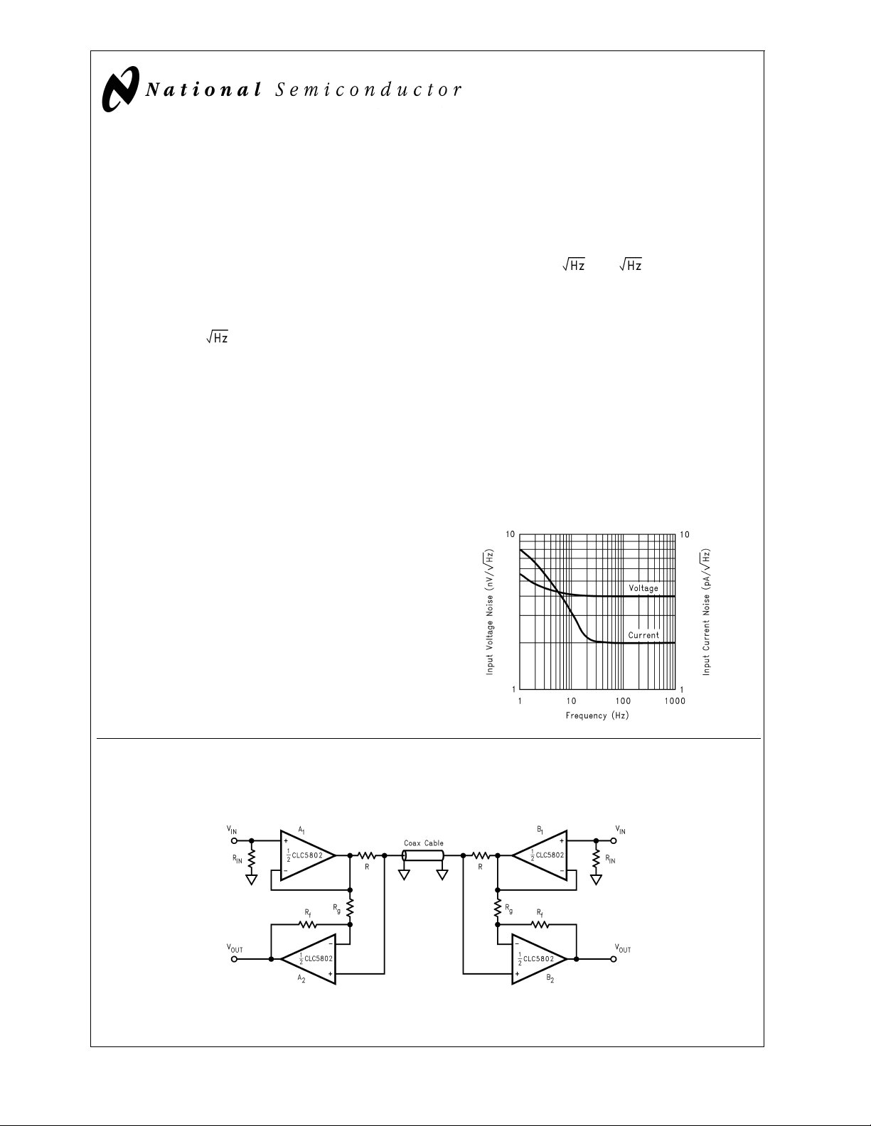
Equivalent Input Noise
DS101341-16
Typical Application
Full Duplex Transmission
DS101341-28
© 2000 National Semiconductor Corporation DS101341 www.national.com
Page 2
Connection Diagram
CLC5802
8-Pin SOIC
DS101341-2
Top View
Ordering Information
Package Part Number Packaging
Marking
8-pin SOIC CLC5802IM CLC5802IM Rails M08A
CLC5802IMX CLC5802IM 2.5k Tape and Reel
Transport Media NSC
Drawing
www.national.com 2
Page 3
CLC5802
Absolute Maximum Ratings (Note 1)
If Military/Aerospace specified devices are required,
Storage Temperature −65˚C to +150˚C
Lead Temperature (soldering 10 sec) +300˚C
please contact the National Semiconductor Sales Office/
Distributors for availability and specifications.
Supply Voltage
±
7V
Short Circuit Current (Note 3)
±
±
V
CC
10V
Common-Mode Input Voltage
Differential Input Voltage
Maximum Junction Temperature +125˚C
Operating Rating(Note 1)
Thermal Resistance (θ
Thermal Resistance (θ
Temperature Range −40˚C to +85˚C
Supply Voltage Range 5V to 12V
) 40˚C/W
JC
) 115˚C/W
JA
Electrical Characteristics
(TA= +25˚C, VCC=±5V, AV= +2V/V, Rf= 100Ω,Rg= 100Ω,RL= 100Ω; unless specified).
Symbol Parameter Conditions Typ Min/Max Ratings
(Note 2)
+25˚C +25˚C 0˚C to
+70˚C
−40˚C
to
+85˚C
Frequency Domain Response
GBW Gain Bandwidth Product V
SSBW −3dB Bandwidth (A
−3dB Bandwidth (A
= +1) V
V
= +2) V
V
LSBW −3dB Bandwidth V
GFP Gain Flatness Peaking DC to 200MHz, V
GFR Gain Flatness Rolloff DC to 20MHz, V
<
0.5V
OUT
OUT
OUT
OUT
V
PP
V
PP
PP
<
0.5V
PP
<
0.5V
PP
<
5.0V
PP
<
0.5
OUT
<
0.5
OUT
120 90
140 110
75 50
40 25
0.0 0.6 dB
0.05 0.5 dB
LPD Linear Phase Deviation DC to 20MHz 0.2 1.0 Deg
Time Domain Response
TRS Rise and Fall Time 1V step 6 8 ns
TSS Settling Time 2V step to 0.1% 18 22 ns
OS Overshoot 1V step 1 5 %
SR Slew Rate 5V step 450 275 V/µs
Distortion And Noise Response
HD2 2nd Harmonic Distortion 1V
HD3 3rd Harmonic Distortion 1V
, 5MHz −69 −57 dBc
PP
, 5MHz −66 −54 dBc
PP
VN Equivalent Input Noise Voltage 1MHz to 100MHz 4.0 4.5 nV/
Units
MHz
ICN Equivalent Input Noise Current 1MHz to 100MHz 2.0 3.0 pA/
CT Crosstalk Input referred, 10MHz −61 −58 dB
Static, DC Performance
AOL Open-Loop Gain DC 60 56 50 50 dB
VIO Input Offset Voltage (Note 4)
±
1.0
±
2.0
±
3.0
±
3.5 mV
DVIO Offset Voltage Average Drift 5 – 15 20 µV/˚C
IB Input Bias Current (Note 4) 1.5 25 40 65 µA
DIB Bias Current Average Drift 150 – 600 700 nA/˚C
IIO Input Offset Current 0.3 3 5 5 µA
DIIO Offset Current Average Drift 5 – 25 50 nA/˚C
PSRR Power Supply Rejection Ratio DC 63 57 55 55 dB
CMRR Common Mode Rejection Ratio DC 60 54 52 52 dB
ICC Supply Current (Note 4) Per Channel, R
∞
=
L
11 12 13 15 mA
www.national.com3
Page 4
Electrical Characteristics (Continued)
(TA= +25˚C, VCC=±5V, AV= +2V/V, Rf= 100Ω,Rg= 100Ω,RL= 100Ω; unless specified).
CLC5802
Symbol Parameter Conditions Typ Min/Max Ratings
+25˚C +25˚C 0˚C to
Miscellaneous Performance
RINC Input Resistance Common-Mode 500 250 125 125 kΩ
RIND Differential-Mode 200 50 25 25 kΩ
CINC Input Capacitance Common-Mode 2.0 3.0 3.0 3.0 pF
CIND Differential-Mode 2.0 3.0 3.0 3.0 pF
ROUT Output Resistance Closed Loop 0.05 0.1 0.2 0.2 Ω
VO Output Voltage Range R
VOL R
CMIR Input Voltage Range Common-Mode
IO Output Current
Note 1: “Absolute Maximum Ratings” are those values beyond which the safety of the device cannot be guaranteed. They are not meant to imply that the devices
should be operated at these limits. The table of “Electrical Characteristics” specifies conditions of device operation. Operating Ratings indicate conditions for which
the device is intended to be functional, but specific performance is not guaranteed,
Note 2: Min/max ratings are based on product characterization and simulation. Individual parameters are tested as noted. Outgoing quality levels are determined
from tested parameters.
Note 3: Output is short circuit protected to ground, however maximum reliability is obtained if output current does not exceed 160mA.
Note 4: 100% tested at +25˚C.
=
L
= 100Ω
L
∞
±
±
±
±
3.6
3.4
3.7
70
±
3.5
±
3.2
±
3.5
±
50
(Note 2)
+70˚C
±
3.3
±
2.6
±
3.3
±
40
−40˚C
to
+85˚C
±
3.3 V
±
1.3 V
±
3.3 V
±
20 mA
Units
www.national.com 4
Page 5

CLC5802
Typical Performance Characteristics (T
unless otherwise specified).
Non-Inverting Frequency Response
DS101341-3
Frequency Response vs. Load Resistance
= 25˚C, VCC=±5V, Rg= 26.1Ω,Rf= 499Ω,RL= 100Ω,
A
Inverting Frequency Response
DS101341-4
Frequency Response vs. Output Amplitude
Frequency Response vs. Capacitive Load
DS101341-5
DS101341-7
DS101341-6
Gain Flatness & Linear Phase Deviation
DS101341-8
www.national.com5
Page 6

Typical Performance Characteristics (T
unless otherwise specified).. (Continued)
CLC5802
Maximum Output Voltage vs. Load
= 25˚C, VCC=±5V, Rg= 26.1Ω,Rf= 499Ω,RL= 100Ω,
A
Channel-to-Channel Crosstalk
Open-Loop Gain & Phase
2nd Harmonic Distortion vs. Output Voltage
DS101341-9
DS101341-11
DS101341-10
2nd and 3rd Harmonic Distortion
DS101341-12
3rd Harmonic Distortion vs. Output Voltage
DS101341-13
www.national.com 6
DS101341-14
Page 7

CLC5802
Typical Performance Characteristics (T
unless otherwise specified).. (Continued)
Closed-Loop Output Resistance
DS101341-15
2-Tone, 3rd order Intermodulation Intercept
= 25˚C, VCC=±5V, Rg= 26.1Ω,Rf= 499Ω,RL= 100Ω,
A
Equivalent Input Noise
DS101341-16
Pulse Response (V
OUT
= 100mV)
Pulse Response (V
OUT
= 2V)
DS101341-18
DS101341-17
Settling Time vs. Capacitive Load
DS101341-19
DS101341-20
www.national.com7
Page 8

Typical Performance Characteristics (T
unless otherwise specified).. (Continued)
CLC5802
Short-Term Settling Time
= 25˚C, VCC=±5V, Rg= 26.1Ω,Rf= 499Ω,RL= 100Ω,
A
CMRR and PSRR
Typical DC Errors vs. Temperature
Output Voltage vs. Output Sinking Current
DS101341-21
DS101341-23
DS101341-22
Output Voltage vs. Output Sourcing Current
DS101341-37
DS101341-38
www.national.com 8
Page 9

Application Information
Low Noise Design
Ultimate low noise performance from circuit designs using
the CLC5802 requires the proper selection of external resistors. By selecting appropriate low-valued resistors for R
R
, amplifier circuits using the CLC5802 can achieve output
g
noise that is approximately the equivalent voltage input
noise of 4nV/
multiplied by the desired gain (AV).
Each amplifier in the CLC5802 has an equivalent input noise
resistance which is optimum for matching source impedances of approximately 2k. Using a transformer, any source
can be matched to achieve the lowest noise design.
For even lower noise performance than the CLC5802, consider the CLC425, CLC426 or CLC5801 at 1.05, 1.6 and
2nV/
, respectively.
DC Bias Currents and Offset Voltages
Cancellation of the output offset voltage due to input bias
currents is possible with the CLC5802. This is done by making the resistance seen from the inverting and non-inverting
inputs equal. Once done, the residual output offset voltage
will be the input offset voltage (V
gain (A
). Application Note OA-7 offers several solutions to
V
) multiplied by the desired
OS
further reduce the output offset.
Output and Supply Considerations
±
With
5V supplies, the CLC5802 is capable of a typical out-
put swing of
±
3.6V under a no-load condition. Additional output swing is possible with slightly higher supply voltages. For
loads of less than 50Ω, the output swing will be limited by the
CLC5802’s output current capability, typically 70mA.
Output settling time when driving capacitive loads can be improved by the use of a series output resistor. See the plot labeled “Settling Time vs. Capacitive Load” in the Typical Performance Characteristics section.
Layout
Proper power supply bypassing is critical to insure good high
frequency performance and low noise. De-coupling capacitors of 0.1µF should be placed as close as possible to the
power supply pins. The use of surface mounted capacitors is
recommended due to their low series inductance.
A good high frequency layout will keep power supply and
ground traces away from the inverting input and output pins.
Parasitic capacitance from these nodes to ground causes
frequency response peaking and possible circuit oscillation.
See OA-15 for more information. National suggests the
CLC730038 (through-hole) or the CLC730036 (SOIC) dual
op amp evaluation board as a guide for high frequency layout and as an aid in device evaluation.
Full Duplex Digital or Analog Transmission
Simultaneous transmission and reception of analog or digital
signals over a single coaxial cable or twisted-pair line can reduce cabling requirements. The CLC5802’s wide bandwidth
and high common-mode rejection in a differential amplifier
configuration allows full duplex transmission of video, telephone, control and audio signals.
In the circuit shown in
Figure 1
, one of the CLC5802’s amps
is used as a “driver” and the other as a difference “receiver”
amplifier. The output impedance of the “driver” is essentially
zero. The two R’s are chosen to match the characteristic impedance of the transmission line. The “driver” op amp gain
can be selected for unity or greater.
Receiver amplifier A
) is connected across R and forms
2(B2
a differential amplifier for the signals transmitted by driver A
f
and
CLC5802
(B1). If the coax cable is lossless and Rfequals Rg, receiver
A
) will then reject the signals from driver A1(B1) and
2(B2
pass the signals from driver B
FIGURE 1.
The output of the receiver amplifier will be:
Care must be given to layout and component placement to
maintain a high frequency common-mode rejection. The plot
of
Figure 2
show the simultaneous reception of signals trans-
mitted at 1MHz and 10MHz.
FIGURE 2.
Five Decade Integrator
A composite integrator, shown in
CLC5802 dual op amp to increase the circuits usable frequency range of operation. The transfer function of this circuit is:
FIGURE 3.
1
1(A1
).
Figure 3
DS101341-28
(1)
DS101341-25
, uses the
(2)
DS101341-27
www.national.com9
Page 10

Application Information (Continued)
A resistive divider made from the 143Ω and 60.4Ω resistors
CLC5802
was chosen to reduce the loop-gain and stabilize the network. The CLC5802 composite integrator provides integration over five decades of operation. R and C set the integrator’s gain.
response of the circuit in
360pF.
K: R2/(R1 + R2)
A
: Op amp low Frequency open loop gain
0
Positive Peak Detector
The CLC5802’s dual amplifiers can be used to implement a
unity-gain peak detector circuit as shown in
Figure 4
shows the frequency and phase
Figure 3
with R = 44.2Ω and C =
DS101341-29
FIGURE 4.
Figure 5
DS101341-31
FIGURE 6.
A current source, built around Q1, provides the necessary
bias current for the second amplifier and prevents saturation
when power is applied. The resistor, R, closes the loop while
diode D
V
prevents negative saturation when VINis less than
2
. AMOS-type switch (not shown) can be used to reset the
C
capacitor’s voltage.
The maximum speed of detection is limited by the delay of
the op amp and the diodes. The use of Schottky diodes will
provide faster response.
Adjustable or Bandpass Equalizer
A “boost” equalizer can be made with the CLC5802 by summing a bandpass response with the input signal, as shown in
.
Figure 7
.
DS101341-30
FIGURE 5.
The acquisition speed of this circuit is limited by the dynamic
resistance of the diode when charging C
cuit’s performance is shown in
Figure 6
.Aplotof the cir-
hold
with a 1MHz sinusoi-
dal input.
www.national.com 10
DS101341-32
FIGURE 7.
The overall transfer function is shown in
Equation (3)
.
(3)
To build a boost circuit, use the design Equation 4 and 5.
(4)
(5)
Select R
for high frequency circuits - R
tween 10pF and 2000pF. Use
parallel combination of R
and C using
2
Equation (4)
and Rb. Select Raand Rbby ei-
a
. Use reasonable values
between 10Ω and 5kΩ, C be-
2
Equation (5)
to determine the
ther the 10Ω to 5kΩ criteria or by other requirements based
on the impedance V
by determining the value of K from
is capable of driving. Finish the design
IN
Equation (6)
.
Page 11

Application Information (Continued)
Figure 8
Figure 7
follows: R
KR=50Ω, C = 120pF.
shows an example of the response of the circuit of
, where fOis 2.3MHz. The component values are as
= 2.1kΩ,Rb= 68.5Ω,R2= 4.22kΩ, R = 500Ω,
a
CLC5802
(6)
DS101341-36
FIGURE 8.
www.national.com11
Page 12

Physical Dimensions inches (millimeters) unless otherwise noted
8-Pin SOIC
NS Package Number M08A
CLC5802 Dual Low-Noise, Voltage Feedback Op Amp
LIFE SUPPORT POLICY
NATIONAL’S PRODUCTS ARE NOT AUTHORIZED FOR USE AS CRITICAL COMPONENTS IN LIFE SUPPORT
DEVICES OR SYSTEMS WITHOUT THE EXPRESS WRITTEN APPROVAL OF THE PRESIDENT AND GENERAL
COUNSEL OF NATIONAL SEMICONDUCTOR CORPORATION. As used herein:
1. Life support devices or systems are devices or
systems which, (a) are intended for surgical implant
into the body, or (b) support or sustain life, and
whose failure to perform when properly used in
accordance with instructions for use provided in the
labeling, can be reasonably expected to result in a
significant injury to the user.
National Semiconductor
Corporation
Americas
Tel: 1-800-272-9959
Fax: 1-800-737-7018
Email: support@nsc.com
www.national.com
National Semiconductor
Europe
Fax: +49 (0) 180-530 85 86
Email: europe.support@nsc.com
Deutsch Tel: +49 (0) 69 9508 6208
English Tel: +44 (0) 870 24 0 2171
Français Tel: +33 (0) 1 41 91 8790
2. A critical component is any component of a life
support device or system whose failure to perform
can be reasonably expected to cause the failure of
the life support device or system, or to affect its
safety or effectiveness.
National Semiconductor
Asia Pacific Customer
Response Group
Tel: 65-2544466
Fax: 65-2504466
Email: ap.support@nsc.com
National Semiconductor
Japan Ltd.
Tel: 81-3-5639-7560
Fax: 81-3-5639-7507
National does not assume any responsibility for use of any circuitry described, no circuit patent licenses are implied and National reserves the right at any time without notice to change said circuitry and specifications.
 Loading...