

Page 1
Features
■
450MHz small signal bandwidth
■
2000 V/µs slew rate
■
5mA / channel supply current
■
-71/-82dBc HD2/HD3 (5MHz)
■
0.03%, 0.03° differential gain, phase
■
70mA output current
■
12ns settling to 0.1%
Applications
■
High performance RGB video
■
Video switchers & routers
■
Video line driver
■
Active filters
■
IF amplifier
■
Twisted pair driver/receiver
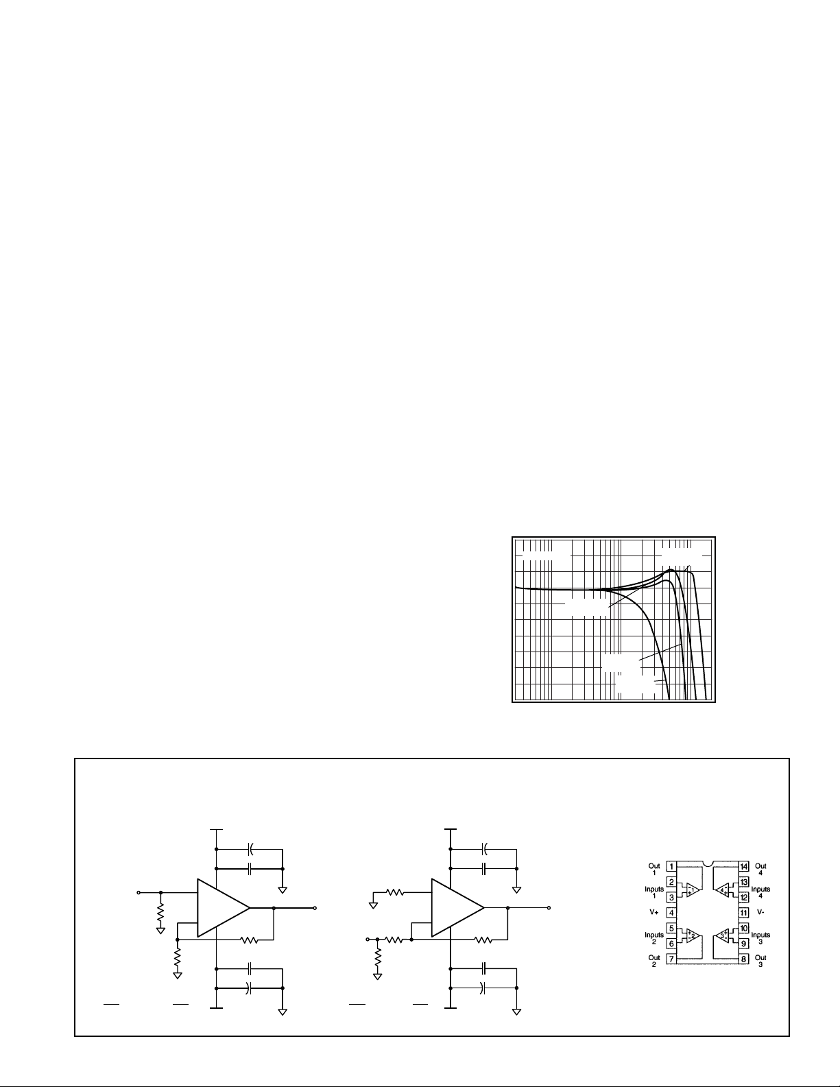
Pinout
DIP & SOIC
General Description
The CLC5654 is a quad, current feedback operational amplifier
that is perfect for many cost-sensitive applications that require
high performance. This device also offers excellent economy
in board space and power, consuming only 5mA per amplifier
while providing 70mA of output current capability. Applications
requiring significant density of high speed devices such as video
routers, matrix switches and high-order active filters will benefit
from the configuration of the CLC5654 and the low channel-tochannel crosstalk of 70dB at 5MHz.
The CLC5654 provides excellent performance for video
applications. Differential gain and phase of 0.03% and 0.03°
makes this device well suited for many professional composite
video systems, but consumer applications will also be able to tak e
advantage of these features due to the device’s low cost. The
CLC5654 offers superior dynamic performance with a small
signal bandwidth of 450MHz and slew rate of 2000V/µs. These
attributes are well suited for many component video applications
such as driving RGB signals down significant lengths of cable.
These and many other application can also take advantage of the
0.1dB flatness to 40MHz.
Combining wide bandwidth with low cost makes the the CLC5654
an attractive option for active filters. SAW filters are often used
in IF filters in the 10’s of MHz range, but higher order filters
designed around a quad operational amplifier may offer an
economical alternative to the typical SAW approach and offer
greater freedom in the selection of filter parameters. National
Semiconductor’s Comlinear Products Group has published
a wide array of liturature on active filters and a list of these
publications can be found on the last page of this datasheet.
CLC5654
Very High-Speed, Low-Cost, Quad Operational Amplifier
N
June 1999
CLC5654
Very High-Speed, Low-Cost, Quad Operational Amplifier
© 1999 National Semiconductor Corporation http://www.national.com
Printed in the U.S.A.
Typical Configurations
Non-Inverting Gain Inverting Gain
Non-Inverting Frequency Response
Vo = 0.25V
pp
Av = +1
Rf = 2.21kΩ
Av = +5
Rf = 402Ω
Av = +10
Normalized Magnitude (0.5dB/div)
1M
Rf = 200Ω
10M
Frequency (Hz)
Av = +2
Rf = 866Ω
100M
V
CC
6.8µF
+
V
in
R
t
R
g
V
o
A1
==+
V
in
R
v
f
R
g
+
1/4
CLC5654
-
V
EE
0.1µF
R
f
0.1µF
6.8µF
V
o
+
V
in
R
t
V
o
A
==−
V
in
R
b
R
g
v
V
CC
6.8µF
+
0.1µF
+
1/4
CLC5654
R
f
0.1µF
R
f
R
g
V
EE
+
6.8µF
V
o
Note: Rb provides DC bias
for the non-inverting input.
Select R
to yield desired
t
Rin = Rt || Rg.
Page 2
http://www.national.com 2
PARAMETERS CONDITIONS TYP MIN/MAX RATINGS UNITS NOTES
Ambient Temperature CLC5654I +25°C +25°C -40 to 85°C
FREQUENCY DOMAIN RESPONSE
-3dB bandwidth A
v
= 1 450 – – MHz
V
o
< 0.5V
pp
350 – – MHz
V
o
< 5V
pp
100 – – MHz
0.1dB bandwidth 40 – – MHz
differential gain NTSC, R
L
= 150Ω 0.03 – – dB
differential phase NTSC, R
L
= 150Ω 0.03 – – dB
TIME DOMAIN RESPONSE
rise and fall time 0.5V step 1.2 – – ns
5V step 2.7 – – ns
settling time to 0.1% 2V step 12 – – ns
overshoot 0.5V step 7 – – %
slew rate 2000 – – V/µs
DISTORTION AND NOISE RESPONSE
2ndharmonic distortion 2Vpp, 5MHz -71 – – dBc
3
rd
harmonic distortion 2Vpp, 5MHz -82 – – dBc
equivalent input noise
voltage (e
ni
) >1MHz 3.3 – – nV/√Hz
non-inverting current (i
bn
) >1MHz 2.5 – – pA/√Hz
inverting current (i
bi
) >1MHz 12 – – pA/√Hz
crosstalk (input inferred) 10MHz 76 – – dBc
STATIC DC PERFORMANCE
input offset voltage 2.5 6 11 mV A
average drift 18 – 55 µV/˚C
input bias current (non-inverting) 6 15 28 µAA
average drift 40 – 160 nA/˚C
input bias current (inverting) 5 12 20 µAA
average drift 25 – 120 nA/˚C
power supply rejection ratio DC 55 47 45 dB
common-mode rejection ratio DC 50 45 43 dB
supply current (per channel) R
L
= ∞ 5 6.7 7 mA A
MISCELLANEOUS PERFORMANCE
input resistance (non-inverting) 1 0.5 0.25 MΩ
input capacitance (non-inverting) 1 2 2 pF
common-mode input range ±2.2 ±2.0 ±1.4 V
output voltage range R
L
= 150Ω ±2.6 ±2.5 ±2.3 V
output current 70 50 40 mA
output resistance, closed loop DC 0.2 0.3 0.6 mΩ
Min/max ratings are based on product characterization and simulation. Individual parameters are tested as noted. Outgoing quality levels are
determined from tested parameters.
CLC5654 Electrical Characteristics
(Av= +2, Rf= 866Ω,RL= 100Ω,Vs= ±5V, unless specified)
Absolute Maximum Ratings
supply voltage (VCC- VEE)
+
14V
output current 95mA
common-mode input voltage
VEEto
V
CC
maximum junction temperature +150°C
storage temperature range -65°C to +150°C
lead temperature (soldering 10 sec) +300°C
Notes
A) J-level:spec is 100% tested at +25°C.
Reliability Information
Transistor Count 152
MTBF (based on limited test data) 12.5Mhr
Ordering Information
Model Temperature Range Description
CLC5654IN -40°C to +85°C 14-pin PDIP
CLC5654IM -40°C to +85°C 14-pin SOIC
CLC5654IMX -40°C to +85°C 14-pin tape and reel
Pac kage Thermal Resistance
Package
θθ
JC
θθ
JA
Plastic (IN) 60°C/W 110°C/W
Surface Mount (IM) 55°C/W 125°C/W
Page 3

3 http://www.national.com
CLC5654 T ypical Performance
(Av= +2, Rf= 866Ω,RL= 100Ω,Vs= ±5V, unless specified)
Non-Inverting Frequency Response
pp
100M100 10k 1M 10M
Phase (deg)
0
-45
-90
-135
-180
-225
100
Noise Current (pA/√Hz)
10
1
Distortion (dBc)
Distortion (dBc)
-100
|/1Ω]
i
/I
o
20 log[|V
Vo = 0.25V
pp
Gain
Av = +1
Rf = 2.21kΩ
Phase
Av = +5
Rf = 402Ω
Av = +10
Normalized Magnitude (0.5dB/div)
1M
Rf = 200Ω
10M
Av = +2
Rf = 866Ω
100M
Frequency (Hz)
Frequency Response vs. V
Vo = 1V
Vo = 2V
Magnitude (1dB/div)
1M
10M
Vo = 4V
o
Vo = 0.1V
pp
pp
pp
100M
Frequency (Hz)
2nd & 3rd Harmonic Distortion, RL = 100Ω
-70
3rd = 5MHz
2nd = 5MHz
-80
3rd = 1MHz
-90
Distortion (dBc)
-100
2nd = 1MHz
-110
012
Output Amplitude (Vpp)
All Hostile Crosstalk
-20
-30
-40
-50
-60
-70
Magnitude (dB)
-80
-90
1M
10M
100M 1000M
Frequency (Hz)
Equivalent Input Noise
100
Inverting Current = 12pA/√Hz
10
Voltage = 3.3nV/√Hz
Noise Voltage (nV/√Hz)
1
1k
Non-Inverting
Current = 2.5pA/√Hz
100k
Frequency (Hz)
Inverting Frequency Response
Vo = 0.25V
pp
Av = -5
Gain
Phase
Normalized Magnitude (1dB/div)
1M
Rf = 402Ω
Av = -1
Rf = 604Ω
Rf = 332Ω
10M
Av = -10
Av = -2
Rf = 523Ω
100M
Frequency (Hz)
2nd & 3rd Harmonic Distortion
-50
Vo = 2V
2nd
RL = 100Ω
pp
3rd
RL = 100Ω
2nd
RL = 1kΩ
-55
-60
-65
-70
-75
-80
-85
-90
-95
1M
3rd
RL = 1kΩ
10M
Frequency (Hz)
2nd & 3rd Harmonic Distortion, RL = 25Ω
-50
2nd = 10MHz
-60
-70
3rd = 10MHz
2nd = 1MHz
3rd = 1MHz
-80
-90
012
Output Amplitude (Vpp)
Most Susceptible Channel Pulse Coupling
Active Channel
Inactive Channel
Active Amplitude (0.5V/div)
Time (50ns/div)
Open-Loop Transimpedance Gain, Z(s)
130
120
110
100
90
Gain
80
70
Phase
60
50
40
30
10k
1M
100M1k 100k 10M
Frequency (Hz)
45
0
-45
-90
-135
-180
-225
-270
-315
-360
-405
Inactive Amplitude (10mV/div)
200
180
160
Phase (degrees)
140
120
100
80
60
40
20
0
Frequency Response vs. R
Vo = 5V
Phase (deg)
Gain
Phase
Magnitude (1dB/div)
1M
2nd & 3rd Harmonic Distortion, RL = 1kΩ
-60
-70
-80
-90
Distortion (dBc)
-100
-110
012
Large & Small Signal Pulse Response
Small Signal
Output Voltage (0.1V/div)
Channel to Channel Gain Matching
Magnitude (0.5dB/div)
1M
Gain Flatness & Linear Phase
0.20
0.10
0
-0.10
-0.20
Magnitude (0.05dB/div)
-0.30
pp
RL = 25Ω
RL = 1kΩ
10M
Frequency (Hz)
3rd = 10MHz
2nd = 10MHz
2nd = 1MHz
3rd = 1MHz
Output Amplitude (Vpp)
Time (10ns/div)
Channel 3
Channel 2
Channel 4
10M
Frequency (Hz)
10
Frequency (MHz)
L
RL = 100Ω
100M
Small Signal
Large Signal
Channel 1
100M
Phase
Gain
Phase (deg)
0
-90
-180
-270
-360
-450
1000M
Output Voltage (0.5V/div)
Large Signal
Phase (deg)
0
-45
-90
-135
-180
-225
0.4
0.3
Phase (deg)
0.2
0.1
0
-0.1
500203040
Page 4

CLC5654
Very High-Speed, Low-Cost, Quad Operational Amplifier
http://www.national.com 4
Customer Design Applications Support
National Semiconductor is committed to design excellence. For sales, literature and technical support, call the
National Semiconductor Customer Response Group at 1-800-272-9959 or fax 1-800-737-7018.
Life Support Policy
National’s products are not authorized for use as critical components in life support devices or systems without the express written approval of
the president of National Semiconductor Corporation. As used herein:
1. Life support devices or systems are devices or systems which, a) are intended for surgical implant into the body, or b) support or
sustain life, and whose failure to perform, when proper ly used in accordance with instructions for use provided in the labeling, can
be reasonably expected to result in a significant injury to the user.
2. A cr itical component is any component of a life support device or system whose failure to perform can be reasonably expected to
cause the failure of the life support device or system, or to affect its safety or effectiveness.
National Semiconductor National Semiconductor National Semiconductor National Semiconductor
Corporation Europe Hong Kong Ltd. Japan Ltd.
1111 West Bardin Road Fax: (+49) 0-180-530 85 86 2501 Miramar Tower Tel:81-043-299-2309
Arlington, TX 76017 E-mail:europe.suppor t.nsc.com 1-23 Kimberley Road Fax: 81-043-299-2408
Tel: 1(800) 272-9959 Deutsch Tel: (+49) 0-180-530 85 85 Tsimshatsui, Kowloon
Fax:1(800) 737-7018 English Tel: (+49) 0-180-532 78 32 Hong Kong
Francais Tel:(+49) 0-180-532 93 58 Tel:(852) 2737-1600
Italiano Tel: (+49) 0-180-534 16 80 Fax: (852) 2736-9960
National does not assume any responsibility for use of any circuitry described, no circuit patent licenses are implied and National reserves the right at any time without notice to change said
circuitry and specifications.
N
Current Feedback Amplifiers
Some of the key features of current feedback
technology are:
■
Independence of AC bandwidth and voltage gain
■
Inherently stable at unity gain
■
Adjustable frequency response with R
f
■
High slew rate
■
Fast settling
Current feedback operation can be described using a
simple equation. The voltage gain for a non-inverting
or inverting current feedback amplifier is approximated
by Equation 1.
Equation 1
where:
Avis the closed loop DC voltage gain
Rfis the feedback resistor
Z(jω) is the open loop transimpedance gain
The denominator of Equation 1 is approximately
equal to 1 at low frequencies. Near the -3dB corner
frequency, the interaction between Rfand Z(jω)
dominates the circuit performance. The value of the
feedback resistor has a large affect on the circuits
performance. Increasing Rfhas the following affects:
■
Decreases loop gain
■
Decreases bandwidth
■
Reduces gain peaking
■
Lowers pulse response overshoot
■
Affects frequency response phase linearity
Layout Considerations
A proper printed circuit layout is essential for achieving
high frequency performance. National provides
evaluation boards f or the CLC5654 (CLC730024 - DIP,
CLC730031 - SOIC) and suggests their use as a guide
for high frequency layout and as an aid for device
testing and characterization. General layout and
supply bypassing play major roles in high frequency
performance. Follow the steps below as a basis for
high frequency layout:
■
Include 6.8µF tantalum and 0.1µF ceramic
capacitors on both supplies.
■
Place the 6.8µF capacitors within 0.75 inches of
the power pins.
■
Place the 0.1µF capacitors less than 0.1 inches
from the power pins.
■
Remove the ground plane under and around the
part, especially near the input and output pins to
reduce parasitic capacitance.
■
Minimize all trace lengths to reduce series
inductances.
■
Use flush-mount printed circuit board pins for
prototyping, never use high profile DIP sockets.
Active Filter Application Notes
OA-21 Simplified Component Pre-Distortion for High
Speed Active Filters
OA-26 Designing High-Speed Active Filters
OA-27 Low-Sensitivity, Lowpass Filter Design
OA-28 Low-Sensitivity, Bandpass Filter Design
with Tuning Method
OA-29 Low-Sensitivity, Highpass Filter Design
with Parasitic Compensation
V
V
A
1
R
Zj
o
i
v
f
=
+
()
ω
 Loading...