

Page 1
Features
■
130mA output current
■
0.05%, 0.03° differential gain, phase
■
3.0mA/ch supply current
■
160MHz bandwidth (Av= +2)
■
-90/-97dBc HD2/HD3 (1MHz)
■
18ns settling to 0.05%
■
370V/µs slew rate
■
Stable for capacitive loads up to 1000pf
■
Single 5V or ±5V supplies
Applications
■
Video line driver
■
ADSL/HDSL driver
■
Coaxial cable driver
■
UTP differential line driver
■
Transformer/coil driver
■
High capacitive load driver
■
Portable/battery-powered applications
■
Differential A/D driver
Typical Application
Differential Line Driver with Load Impedance Conversion
Pinout
DIP & SOIC
General Description
The National CLC5622 has a new output stage that delivers high
output drive current (130mA), but consumes minimal
quiescent supply current (3.0mA/ch) from a single 5V supply. Its
current feedback architecture, fabricated in an advanced complementary bipolar process, maintains consistent performance over
a wide range of gains and signal levels, and has a linear-phase
response up to one half of the -3dB frequency.
The CLC5622 offers 0.1dB gain flatness to 30MHz and differential gain and phase errors of 0.05% and 0.03°. These features are
ideal for professional and consumer video applications.
The CLC5622 offers superior dynamic performance with a
160MHz small-signal bandwidth, 370V/µs slew rate and 4.4ns
rise/fall times (2V
step
). The combination of low quiescent power,
high output current drive, and high-speed performance make
the CLC5622 well suited for many battery-powered personal
communication/computing systems.
The ability to drive low-impedance, highly capacitive loads,
makes the CLC5622 ideal for single ended cable applications.
It also drives low impedance loads with minimum distortion.
The CLC5622 will drive a 100Ω load with only -95/-95dBc
second/third harmonic distortion (Av= +2, V
out
= 2Vpp, f = 1MHz).
With a 25Ω load, and the same conditions, it produces only -72/
-77dBc second/third harmonic distortion.
The CLC5622 can also be used for driving differential-input step-
up transformers for applications such as Asynchronous Digital
Subscriber Lines (ADSL) or High-Bit-Rate Digital Subscriber
Lines (HDSL).
When driving the input of high-resolution A/D converters, the
CLC5622 provides excellent -90/-97dBc second/third harmonic
distortion (Av= +2, V
out
= 2Vpp, f = 1MHz, RL= 1kΩ) and fast
settling time.
CLC5622
Dual, High Output,Video Amplifier
N
June 1999
CLC5622
Dual, High Output, Video Amplifier
© 1999 National Semiconductor Corporation http://www.national.com
Printed in the U.S.A.
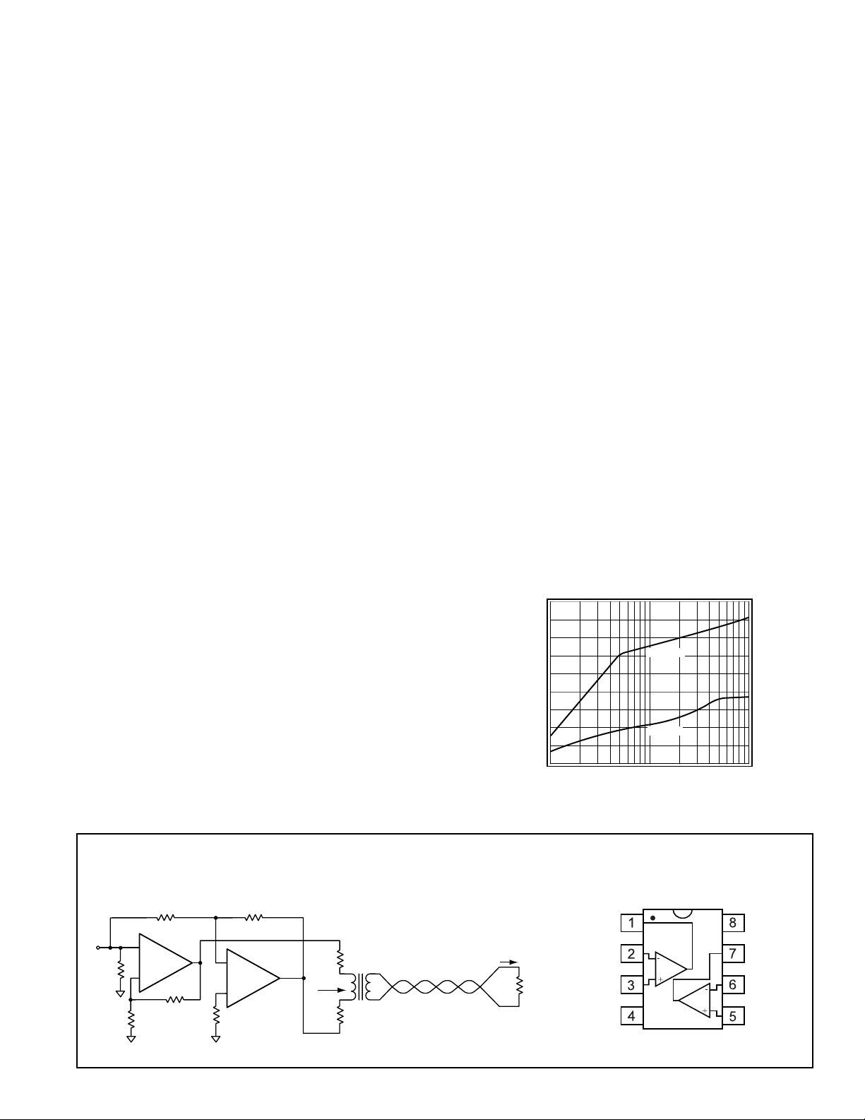
Maximum Output Voltage vs. R
10
9
)
8
pp
7
6
5
4
3
Output Voltage (V
2
1
10
VCC = ±5V
Vs = +5V
100
RL (Ω)
L
1000
R
g2
V
V
in
+
CLC5622
R
t1
-
R
g1
d/2
1/2
R
f1
R
t2
R
-
1/2
CLC5622
+
f2
Vo1
V
1
V
non-inv
-V
inv
1
CC
-V
d/2
R
m/2
1:n
R
eq
R
m/2
Z
UTP
o
I
o
+
R
V
L
o
-
+V
Vo2
V
inv
V
non-inv
CC
2
2
Page 2
http://www.national.com 2
PARAMETERS CONDITIONS TYP MIN/MAX RATINGS UNITS NOTES
Ambient Temperature CLC5622IN/IM +25°C +25°C 0 to 70°C -40 to 85°C
FREQUENCY DOMAIN RESPONSE
-3dB bandwidth V
o
= 0.5V
pp
130 100 90 85 MHz
V
o
= 2.0V
pp
95 80 77 75 MHz
-
0.1dB bandwidth Vo= 0.5V
pp
30 25 20 20 MHz
gain peaking <200MHz, V
o
= 0.5V
pp
0 0.5 0.9 1.3 dB
gain rolloff <30MHz, V
o
= 0.5V
pp
0.1 0.4 0.6 0.6 dB
linear phase deviation <30MHz, V
o
= 0.5V
pp
0.15 0.3 0.4 0.4 deg
differential gain NTSC, R
L
= 150Ω to -1V 0.03 – – – %
differential phase NTSC, R
L
= 150Ω to -1V 0.07 – – – deg
TIME DOMAIN RESPONSE
rise and fall time 2V step 4.5 6.0 6.4 6.8 ns
settling time to 0.05% 1V step 17 25 40 60 ns
overshoot 2V step 11 15 18 18 %
slew rate 2V step 280 195 165 150 V/µs
DISTORTION AND NOISE RESPONSE
2
nd
harmonic distortion 2Vpp, 1MHz -79 -76 -73 -73 dBc
2V
pp
, 1MHz; RL= 1kΩ -80 -78 -75 -75 dBc
2V
pp
, 5MHz -66 -60 -58 -58 dBc
3
rd
harmonic distortion 2Vpp, 1MHz -85 -82 -79 -79 dBc
2V
pp
, 1MHz; RL= 1kΩ -83 -81 -78 -78 dBc
2V
pp
, 5MHz -65 -62 -60 -60 dBc
equivalent input noise
voltage (e
ni
) >1MHz 3.4 4.4 4.9 4.9 nV/√Hz
non-inverting current (i
bn
) >1MHz 6.3 8.2 9.0 9.0 pA/√Hz
inverting current (i
bi
) >1MHz 8.7 11.3 12.4 12.4 pA/√Hz
crosstalk (input referred) 10MHz, 1V
pp
-72 – – – dB
STATIC DC PERFORMANCE
input offset voltage 1 4 6 6 mV A
average drift 8 – – – µV/˚C
input bias current (non-inverting) 6 18 22 24 µAA
average drift 40 – – – nA/˚C
input bias current (inverting) 6 14 16 17 µAA
average drift 25 – – – nA/˚C
power supply rejection ratio DC 48 45 43 43 dB
common-mode rejection ratio DC 47 45 43 43 dB
supply current per channel R
L
= ∞ 3.0 3.4 3.6 3.6 mA A
MISCELLANEOUS PERFORMANCE
input resistance (non-inverting) 0.36 0.26 0.23 0.23 MΩ
input capacitance (non-inverting) 1.8 2.75 2.75 2.75 pF
input voltage range, High 4.2 4.1 4.1 4.0 V
input voltage range, Low 0.8 0.9 0.9 1.0 V
output voltage range, High R
L
= 100Ω 4.0 3.9 3.9 3.8 V
output voltage range, Low R
L
= 100Ω 1.0 1.1 1.1 1.2 V
output voltage range, High R
L
= ∞ 4.1 4.0 4.0 3.9 V
output voltage range, Low R
L
= ∞ 0.9 1.0 1.0 1.1 V
output current 100 80 65 40 mA B
output resistance, closed loop DC 70 105 105 140 mΩ
Min/max ratings are based on product characterization and simulation. Individual parameters are tested as noted. Outgoing quality levels are
determined from tested parameters.
+5V Electrical Characteristics
(Av= +2, Rf= 750Ω,RL= 100Ω,Vs= +5V1,Vcm= VEE+ (Vs/2), RLtied to Vcm, unless specified)
Absolute Maximum Ratings
supply voltage (VCC- VEE)
+
14V
output current (see note C) 140mA
common-mode input voltage
VEEto
V
CC
maximum junction temperature +150°C
storage temperature range -65°C to +150°C
lead temperature (soldering 10 sec) +300°C
ESD rating (human body model) 1000V
Notes
A) J-level:spec is 100% tested at +25°C.
B)The short circuit current can exceed the maximum safe
output current.
1) V
s
= VCC- V
EE
Reliability Information
Transistor Count 98
MTBF (based on limited test data) 300Mhr
Page 3
3 http://www.national.com
PARAMETERS CONDITIONS TYP GUARANTEED MIN/MAX UNITS NOTES
Ambient Temperature CLC5622IN/IM +25°C +25°C 0 to 70°C -40 to 85°C
FREQUENCY DOMAIN RESPONSE
-3dB bandwidth V
o
= 1.0V
pp
160 135 120 115 MHz
V
o
= 4.0V
pp
75 60 57 55 MHz
-
0.1dB bandwidth Vo= 1.0V
pp
30 25 20 20 MHz
gain peaking <200MHz, V
o
= 1.0V
pp
0 0.5 0.9 1.3 dB
gain rolloff <30MHz, V
o
= 1.0V
pp
0.1 0.2 0.3 0.3 dB
linear phase deviation <30MHz, V
o
= 1.0V
pp
0.15 0.3 0.4 0.4 deg
differential gain NTSC, R
L
=150Ω 0.05 0.1 – – %
differential phase NTSC, R
L
=150Ω 0.03 0.06 – – deg
TIME DOMAIN RESPONSE
rise and fall time 2V step 4.4 5.8 6.2 6.8 ns
settling time to 0.05% 2V step 18 25 40 60 ns
overshoot 2V step 19 21 23 24 %
slew rate 2V step 370 280 260 240 V/µs
DISTORTION AND NOISE RESPONSE
2
nd
harmonic distortion 2Vpp, 1MHz -95 -88 -85 -85 dBc
2V
pp
, 1MHz; RL= 1kΩ -90 -88 -85 -85 dBc
2V
pp
, 5MHz -74 -66 -64 -64 dBc
3
rd
harmonic distortion 2Vpp, 1MHz -95 -91 -88 -88 dBc
2V
pp
, 1MHz; RL= 1kΩ -97 -93 -90 -90 dBc
2V
pp
, 5MHz -73 -64 -62 -62 dBc
equivalent input noise
voltage (e
ni
) >1MHz 3.4 4.4 4.9 4.9 nV/√Hz
non-inverting current (i
bn
) >1MHz 6.3 8.2 9.0 9.0 pA/√Hz
inverting current (i
bi
) >1MHz 8.7 11.3 12.4 12.4 pA/√Hz
crosstalk (input referred) 10MHz, 1V
pp
-72 – – – dB
STATIC DC PERFORMANCE
input offset voltage 1 6 7 8 mV
average drift 10 – – – µV/˚C
input bias current (non-inverting) 8 18 23 25 µA
average drift 40 – – – nA/˚C
input bias current (inverting) 9 24 28 28 µA
average drift 30 – – – nA/˚C
power supply rejection ratio DC 48 45 43 43 dB
common-mode rejection ratio DC 48 46 44 44 dB
supply current (per channel) R
L
= ∞ 3.2 3.8 4.0 4.0 mA
MISCELLANEOUS PERFORMANCE
input resistance (non-inverting) 0.48 0.34 0.31 0.31 MΩ
input capacitance (non-inverting) 1.45 2.15 2.15 2.15 pF
common-mode input range
±
4.2
±
4.1
±
4.1
±
4.0 V
output voltage range R
L
= 100Ω
±
3.8
±
3.6
±
3.6
±
3.5 V
output voltage range R
L
= ∞
±
4.0
±
3.8
±
3.8
±
3.7 V
output current 130 100 80 50 mA B
output resistance, closed loop DC 60 90 90 120 mΩ
±5V Electrical Characteristics
(Av= +2, Rf= 750Ω,RL= 100Ω,VCC= ±5V, unless specified)
Notes
B)The short circuit current can exceed the maximum safe
output current.
Ordering Information
Model Temperature Range Description
CLC5622IN -40°C to +85°C 8-pin PDIP
CLC5622IM -40°C to +85°C 8-pin SOIC
CLC5622IMX -40°C to +85°C 8-pin SOIC tape and reel
Pac kage Thermal Resistance
Package
θθ
JC
θθ
JA
Plastic (IN) 65°C/W 130°C/W
Surface Mount (IM) 50°C/W 145°C/W
Page 4
http://www.national.com 4
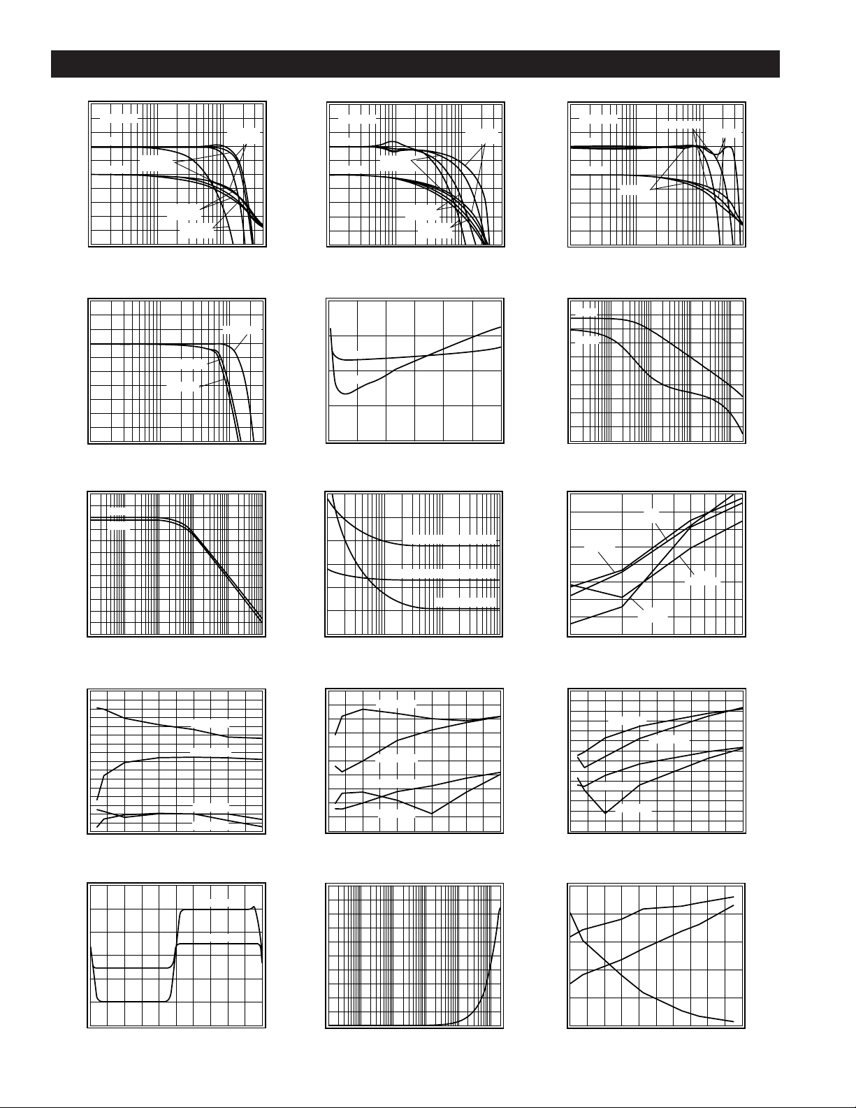
+5V T ypical Performance
(Av= +2, Rf= 750Ω,RL= 100Ω,Vs= +5V1,Vcm= VEE+ (Vs/2), RLtied to Vcm, unless specified)
Non-Inverting Frequency Response
Vo = 0.5V
pp
Gain
Av = +1
Rf = 1.2kΩ
Phase
Av = +5
Rf = 402Ω
Av = +10
10M
Rf = 200Ω
100M
Normalized Magnitude (1dB/div)
1M
Frequency (Hz)
Frequency Response vs. V
Vo = 1V
Vo = 2V
o
pp
pp
Magnitude (1dB/div)
1M
10M
100M
Frequency (Hz)
PSRR & CMRR
60
PSRR
50
CMRR
40
30
20
PSRR & CMRR (dB)
10
0
1k 10k 100M
100k 1M 10M
Frequency (Hz)
2nd & 3rd Harmonic Distortion, RL = 25Ω
-40
-45
-50
-55
-60
3rd, 10MHz
2nd, 10MHz
-65
Distortion (dBc)
-70
-75
-80
2nd, 1MHz
3rd, 1MHz
0 0.5 1 1.5 2 2.5
Output Amplitude (Vpp)
Large & Small Signal Pulse Response
Large Signal
Small Signal
Output Voltage (0.5V/div)
Time (10ns/div)
Av = +2
Rf = 649Ω
Vo = 0.1V
pp
Phase (deg)
0
-90
-180
-270
-360
-450
Inverting Frequency Response
Vo = 0.5V
pp
Gain
Av = -2
Rf = 649Ω
Phase
Av = -5
Rf = 402Ω
Av = -10
10M
Rf = 200Ω
100M
Normalized Magnitude (1dB/div)
1M
Frequency (Hz)
Gain Flatness & Linear Phase
Gain
Phase
Magnitude (0.1dB/div)
0
10
20
Frequency (MHz)
Equivalent Input Noise
3.6
3.5
3.4
3.3
Inverting Current 10.8pA/√Hz
Non-Inverting Current 7.6pA/√Hz
3.2
3.1
Noise Voltage (nV/√Hz)
3.0
10k 100k 1M 10M
Voltage 3.1nV/√Hz
Frequency (Hz)
2nd & 3rd Harmonic Distortion, RL = 100Ω
-50
3rd, 10MHz
-60
-70
2nd, 10MHz
-80
Distortion (dBc)
-90
2nd, 1MHz
3rd, 1MHz
-100
0 0.5 1 1.5 2 2.5
Output Amplitude (Vpp)
Output Impedance vs. Frequency
50
40
30
20
10
Output Impedance (Ω)
0
10k 100k 1M 10M
1k
Frequency (Hz)
Av = -1
Rf = 1kΩ
100M
180
135
90
45
0
-45
0.3
0.2
0.1
0
-0.1
30
15
11
7
3
Phase (deg)
Frequency Response vs. R
Vo = 0.5V
pp
Gain
Phase
RL = 25Ω
RL = 1kΩ
L
Phase (deg)
RL = 100Ω
0
-90
-180
Magnitude (1dB/div)
-270
-360
-450
1M
10M
100M
Frequency (Hz)
Open Loop Transimpedance Gain, Z(s)
120
Gain
100
Phase (deg)
Phase
80
60
Magnitude (dBΩ)
40
20
10k 100k 1M 10M 100M
220
180
Phase (deg)
140
100
60
20
Frequency (Hz)
2nd & 3rd Harmonic Distortion
-60
Vo = 2V
2nd
RL = 1kΩ
pp
3rd
RL = 100Ω
2nd
RL = 100Ω
3rd
RL = 1kΩ
Noise Current (pA/√Hz)
Distortion (dBc)
-70
-80
-90
-100
1M
10M
Frequency (Hz)
2nd & 3rd Harmonic Distortion, RL = 1kΩ
-50
-60
-70
3rd, 10MHz
2nd, 10MHz
-80
-90
-100
Distortion (dBc)
-110
2nd, 1MHz
3rd, 1MHz
-120
0 0.5 1 1.5 2 2.5
Output Amplitude (Vpp)
IBI, IBN, VIO vs. Temperature
-1.5 4
I
1.0 3
(mV)
IO
0.5 2
BI
I
BI
, I
V
IO
BN
(µA)
01
I
-0.5 0
Offset Voltage V
-1
BN
-1
-60 -20 20 60 100 140
Temperature (°C)
Page 5

5 http://www.national.com
±5V T ypical Performance
(Av= +2, Rf= 750Ω,RL= 100Ω,VCC= ±5V, unless specified)
Frequency Response
Vo = 1.0V
pp
Gain
Av = +1
Rf = 1.2kΩ
Phase
Av = +5
Rf = 402Ω
Av = +10
Normalized Magnitude (1dB/div)
1M
Rf = 200Ω
10M
100M
Av = +2
Rf = 649Ω
Frequency (Hz)
Frequency Response vs. V
Vo = 5V
Vo = 2V
o
Vo = 0.1V
pp
pp
pp
Vo = 1V
Magnitude (1dB/div)
1M
10M
100M
Frequency (Hz)
Large Signal Pulse Response
Av = +2
Amplitude (0.5V/div)
Av = -2
Time (10ns/div)
2nd & 3rd Harmonic Distortion, RL = 25Ω
-40
-50
-60
-70
Distortion (dBc)
3rd, 10MHz
2nd, 10MHz
2nd, 1MHz
-80
-90
012345
3rd, 1MHz
Output Amplitude (Vpp)
Short Term Settling Time
0.2
0.15
0.1
0.05
0
-0.05
(% Output Step)
o
-0.1
V
-0.15
-0.2
1 10 100 1000 10000
Time (ns)
0
-45
-90
-135
-180
-225
pp
Inverting Frequency Response
Phase (deg)
Vo = 1.0V
Gain
Phase
Normalized Magnitude (1dB/div)
1M
Gain Flatness & Linear Phase
Gain
Phase
Magnitude (0.1dB/div)
0
5
Differential Gain & Phase
0.1
Gain Pos Sync
Gain (%)
-0.6
Gain Neg Sync
1234
Number of 150 Ω Loads
2nd & 3rd Harmonic Distortion, RL = 100Ω
-60
-70
-80
Distortion (dBc)
-90
-100
0 0.5 1 1.5 2 2.5
Output Amplitude (Vpp)
Long Term Settling Time
0.2
0.15
0.1
0.05
0
-0.05
(% Output Step)
o
-0.1
V
-0.15
-0.2
1
µ
10µ100µ1m 100m
Frequency Response vs. R
pp
Rf = 649Ω
Av = -1
Rf = 1.2kΩ
Av = -5
Rf = 500Ω
Av = -10
Rf = 500Ω
10M
100M
Frequency (Hz)
10 15 20 30
Av = -2
25
Phase (deg)
180
135
90
45
0
-45
0.3
0.2
Phase (deg)
0.1
0
-0.1
Vo = 1.0V
pp
Gain
Phase
Magnitude (1dB/div)
1M
RL = 100Ω
RL = 25Ω
10M
Frequency (Hz)
Small Signal Pulse Response
Av = +2
Amplitude (200mV/div)
Av = -2
Time (10ns/div)
Frequency (MHz)
2nd & 3rd Harmonic Distortion
-50
Vo = 2V
pp
-60
Phase (deg)
-70
2nd
RL = 1kΩ
-80
Distortion (dBc)
-90
-100
1M
3rd
RL = 1kΩ
Phase Neg Sync
Phase Pos Sync
0.01
00
-0.01-0.1
-0.02-0.2
-0.03-0.3
-0.04-0.4
-0.05-0.5
-0.06
Frequency (Hz)
2nd & 3rd Harmonic Distortion, RL = 1kΩ
-50
3rd, 10MHz
2nd, 10MHz
-60
-70
-80
-90
-100
2nd, 1MHz
3rd, 1MHz
Distortion (dBc)
-110
-120
012345
Output Amplitude (Vpp)
IBI, IBN, VOS vs. Temperature
4
Time (s)
10m
(mV)
36
OS
22
1-2
Offset Voltage V
0
-100 -50 0 50 100 150
I
BI
V
OS
I
BN
Temperature (°C)
L
RL = 1kΩ
100M
3rd
RL = 100Ω
RL = 100Ω
3rd, 10MHz
2nd, 10MHz
2nd, 1MHz
3rd, 1MHz
2nd
0
-90
-180
-270
-360
-450
10M
10
-6
Phase (deg)
I
BI
, I
BN
(µA)
Page 6

http://www.national.com 6
±5V Typical Channel Matching Performance
(Av= +2, Rf= 750Ω,RL= 100Ω,VCC= ±5V, unless specified)
CLC5622 OPERATION
The CLC5622 is a current feedback amplifier built in an
advanced complementary bipolar process. The CLC5622
operates from a single 5V supply or dual ±5V supplies.
Operating from a single supply, the CLC5622 has the
following features:
■
Provides 100mA of output current while
consuming 15mW of power
■
Offers low -80/-83dB 2nd and 3rd harmonic
distortion
■
Provides BW > 80MHz and 1MHz distortion
< -75dBc at Vo = 2V
pp
The CLC5622 performance is further enhanced in ±5V
supply applications as indicated in the
±5V Electrical
Characteristics
table and
±5V Typical Performance
plots.
Current Feedback Amplifiers
Some of the key features of current feedback technology
are:
■
Independence of AC bandwidth and voltage gain
■
Inherently stable at unity gain
■
Adjustable frequency response with feedbac k resistor
■
High slew rate
■
Fast settling
Current feedback operation can be described using a simple
equation. The voltage gain for a non-inverting or inverting
current feedback amplifier is approximated by Equation 1.
Equation 1
where:
■
Avis the closed loop DC voltage gain
■
Rfis the feedback resistor
■
Z(jω) is the CLC5622’s open loop
transimpedance gain
■
is the loop gain
The denominator of Equation 1 is approximately equal to
1 at low frequencies. Near the -3dB corner frequency, the
interaction between Rfand Z(jω) dominates the circuit
performance. The value of the feedback resistor has a
large affect on the circuits performance. Increasing R
f
has the following affects:
■
Decreases loop gain
■
Decreases bandwidth
■
Reduces gain peaking
■
Lowers pulse response overshoot
■
Affects frequency response phase linearity
Refer to the
Feedback Resistor Selection
section for
more details on selecting a feedback resistor value.
V
V
A
1
R
Z(j )
o
in
v
f
=
+
ω
Zj
R
f
ω
()
CLC5622 DESIGN INFORMATION
Single Supply Operation (VCC= +5V, VEE= GND)
The specifications given in the
+5V Electrical Character-
istics
table for single supply operation are measured with
a common mode voltage (Vcm) of 2.5V. Vcmis the voltage around which the inputs are applied and the
output voltages are specified.
Operating from a single +5V supply, the Common Mode
Input Range (CMIR) of the CLC5622 is typically +0.8V to
+4.2V. The typical output range with RL=100Ω is +1.0V
to +4.0V.
For single supply DC coupled operation, keep input
signal levels above 0.8V DC. For input signals that drop
below 0.8V DC, AC coupling and level shifting the signal
are recommended. The non-inverting and inverting
configurations for both input conditions are illustrated in
the following 2 sections.
Channel Matching
Magnitude (0.5dB/div)
1M 10M 100M
Frequency (Hz)
Channel 2
Channel 1
Input Referred Crosstalk
-20
Vo = 1V
-30
-40
-50
-60
-70
Magnitude (dB)
-80
-90
pp
1M
Frequency (Hz)
Pulse Crosstalk
Active Output
Channel
Inactive Output
Channel
Active Channel
Amplitude (0.2V/div)
10M 100M
Time (10ns/div)
Amplitude (20mV/div)
Inactive Channel
Page 7

DC Coupled Single Supply Operation
Figures 1 and 2 show the recommended non-inverting
and inverting configurations for input signals that remain
above 0.8V DC.
Figure 1: Non-Inverting Configuration
Figure 2: Inverting Configuration
AC Coupled Single Supply Operation
Figures 3 and 4 show possible non-inverting and inverting configurations for input signals that go below 0.8V
DC. The input is AC coupled to prevent the need for
level shifting the input signal at the source. The resistive
voltage divider biases the non-inverting input to VCC÷2
= 2.5V (For VCC= +5V).
Figure 3: AC Coupled Non-Inverting Configuration
Figure 4: AC Coupled Inverting Configuration
Dual Supply Operation
The CLC5622 operates on dual supplies as well as
single supplies. The non-inverting and inverting configurations are shown in Figures 5 and 6.
Figure 5: Dual Supply Non-Inverting Configuration
Figure 6: Dual Supply Inverting Configuration
7 http://www.national.com
V
3
2
R
g
CC
8
+
1/2
CLC5622
-
4
6.8µF
+
0.1µF
1
R
f
V
o
A1
==+
V
in
V
o
R
L
V
cm
R
f
v
R
g
Note: Rt, RL and Rg are tied
to Vcm for minimum power
consumption and maximum
output swing.
V
in
R
t
V
cm
V
cm
V
A
3
CLC5622
2
v
CC
6.8µF
+
0.1µF
8
+
+
1/2
-
-
4
R
R
Select Rt to yield
f
desired Rin = Rt || R
R
g
1
f
V
o
R
L
V
cm
g
Note: Rb, provides DC bias
for non-inverting input.
Rb, RL and Rt are tied
to Vcm for minimum power
consumption and maximum
output swing.
R
b
V
cm
R
cm
g
R
t
V
o
V
in
V
in
V
==−
V
CC
6.8µF
+
V
CC
2
C
c
V
in
R
R
0.1µF
8
3
+
1/2
g
CLC5622
2
-
1
4
R
f
V
o
R
R
VV
=−
o
low frequencycutoff
f
2.5
+
in
R
g
=
2RC
1
π
gc
V
CC
6.8µF
+
0.1µF
V
in
R
t
3
2
R
g
8
+
1/2
CLC5622
-
4
V
EE
1
R
f
0.1µF
6.8µF
V
o
V
o
A1
==+
V
in
+
R
v
f
R
g
V
CC
6.8µF
+
R
c
3
R
2
R
g
8
+
1/2
CLC5622
-
4
0.1µF
1
R
f
V
o
C
1
π
c
in
,where: R
==
2RC
R
RR
>>
in
2
source
V
in
R
f
VV1
=+
o
in
+
R
g
low frequencycutoff
V
C
CC
2
2.5
V
CC
6.8µF
+
8
+
1/2
CLC5622
-
4
V
EE
0.1µF
1
R
f
0.1µF
6.8µF
Note: Rb provides DC bias
for the non-inverting input.
Select R
Rin = Rt || Rg.
+
V
o
to yield desired
t
V
in
R
t
V
o
A
==−
V
in
R
b
3
2
R
g
R
f
v
R
g
Page 8

http://www.national.com 8
Feedback Resistor Selection
The feedback resistor, Rf, affects the loop gain and
frequency response of a current feedback amplifier.
Optimum performance of the CLC5622, at a gain of
+2V/V, is achieved with Rfequal to 750Ω. The frequency
response plots in the
Typical Performance
sections
illustrate the recommended Rffor several gains. These
recommended values of Rfprovide the maximum bandwidth with minimal peaking. Within limits, Rfcan be
adjusted to optimize the frequency response.
■
Decrease Rfto peak frequency response and
extend bandwidth
■
Increase Rfto roll off frequency response and
compress bandwidth
As a rule of thumb, if the recommended Rfis doubled,
then the bandwidth will be cut in half.
Unity Gain Operation
The recommended Rffor unity gain (+1V/V) operation
is 1.2kΩ.Rgis left open. Parasitic capacitance at the
inverting node may require a slight increase in Rfto
maintain a flat frequency response.
Load Termination
The CLC5622 can source and sink near equal amounts
of current. For optimum performance, the load should be
tied to Vcm.
Driving Cables and Capacitive Loads
When driving cables, double termination is used to
prevent reflections. For capacitive load applications, a
small series resistor at the output of the CLC5622 will
improve stability and settling performance. The
Frequency Response vs. C
L
plot, shown below in
Figure 7, gives the recommended series resistance value
for optimum flatness at various capacitive loads.
Figure 7: Frequency Response vs. C
L
Transmission Line Matching
One method for matching the characteristic impedance
(Zo) of a transmission line or cable is to place the
appropriate resistor at the input or output of the amplifier.
Figure 8 shows typical inverting and non-inverting circuit
configurations for matching transmission lines.
Non-inverting gain applications:
■
Connect Rgdirectly to ground.
■
Make R1, R2, R6, and R7equal to Zo.
■
Use R3to isolate the amplifier from reactive
loading caused by the transmission line,
or by parasitics.
Figure 8:Transmission Line Matching
Inverting gain applications:
■
Connect R3directly to ground.
■
Make the resistors R4, R6, and R7equal to Zo.
■
Make R5II Rg= Zo.
The input and output matching resistors attenuate the
signal by a factor of 2, therefore additional gain is needed.
Use C6to match the output transmission line over a
greater frequency range. C6compensates for the increase
of the amplifier’s output impedance with frequency.
Power Dissipation
Follow these steps to determine the power consumption
of the CLC5622:
1. Calculate the quiescent (no-load) power:
P
amp
= ICC(VCC- VEE)
2. Calculate the RMS power at the output stage:
Po= (VCC- V
load
) (I
load
), where V
load
and I
load
are the RMS voltage and current across the
external load.
3. Calculate the total RMS power:
Pt= P
amp
+ P
o
The maximum power that the DIP and SOIC packages
can dissipate at a given temperature is illustrated in
Figure 9. The power derating curve for any CLC5622
package can be derived by utilizing the following
equation:
where
T
amb
= Ambient temperature (°C)
θJA= Thermal resistance, from junction to ambient,
for a given package (°C/W)
Vo = 1V
pp
CL = 10pF
Rs = 68.1Ω
CL = 100pF
Rs = 17.4Ω
CL = 1000pF
Rs = 6.7Ω
+
R
-
Magnitude (1dB/div)
1k
1M
s
C
L
1k
Frequency (Hz)
10M
1k
100M
C
Z
R
1
+
V
1
R
4
+
V
2
-
0
Z
0
R
3
+
1/2
CLC5622
R
2
-
R
R
5
R
g
f
6
Z
0
R
6
V
o
R
7
(175 T
°− )
amb
θ
JA
Page 9

9 http://www.national.com
Figure 9: Power Derating Curves
Layout Considerations
A proper printed circuit layout is essential for achieving
high frequency performance. Comlinear provides
evaluation boards for the CLC5622 (CLC730038-DIP,
CLC730036-SOIC) and suggests their use as a guide for
high frequency layout and as an aid f or de vice testing and
characterization.
General layout and supply bypassing play major roles in
high frequency performance. Follow the steps below as
a basis for high frequency layout:
■
Include 6.8µF tantalum and 0.1µF ceramic
capacitors on both supplies.
■
Place the 6.8µF capacitors within 0.75 inches
of the power pins.
■
Place the 0.1µF capacitors less than 0.1 inches
from the power pins.
■
Remove the ground plane under and around the
part, especially near the input and output pins to
reduce parasitic capacitance.
■
Minimize all trace lengths to reduce series
inductances.
■
Use flush-mount printed circuit board pins for
prototyping, never use high profile DIP sockets.
Evaluation Board Information
A data sheet is available f or the CLC730038/ CLC730036
evaluation boards. The evaluation board data sheet
provides:
■
Evaluation board schematics
■
Evaluation board lay outs
■
General information about the boards
The evaluation boards are designed to accommodate
dual supplies. The boards can be modified to provide
single supply operation. For best performance; 1) do
not connect the unused supply, 2) ground the unused
supply pin.
SPICE Models
SPICE models provide a means to evaluate amplifier
designs. Free SPICE models are available for National’s
monolithic amplifiers that:
■
Support Berkeley SPICE 2G and its many derivatives
■
Reproduce typical DC, AC, Transient, and Noise
performance
■
Support room temperature simulations
The
readme
file that accompanies the diskette lists
released models, and provides a list of modeled parameters. The application note OA-18, Simulation SPICE
Models for National’s Op Amps, contains schematics and
a reproduction of the readme file.
Single Supply Cable Driver
The typical application shown below shows one of the
CLC5622 amplifiers driving 10m of 75Ω coaxial cable.
The CLC5622 is set for a gain of +2V/V to compensate
for the divide-by-two voltage drop at Vo.
Figure 10: Single Supply Cable Driver
Figure 11: Response After 10m of Cable
Single Supply Lowpass Filter
Figures 12 and 13 illustrate a lowpass filter and design
equations. The circuit operates from a single supply of
+5V. The voltage divider biases the non-inverting input to
2.5V. And the input is AC coupled to prevent the need f or
level shifting the input signal at the source. Use the
design equations to determine R1, R2, C1, and C2based
on the desired Q and corner frequency.
Application Circuits
1.0
IN
0.8
0.6
0.4
Power (W)
0.2
0
-40 -20 0 20 40 60 80 100 120 180
IM
140 160
Ambient Temperature (°C)
+5V
6.8µF
+
5kΩ
0.1µF
5kΩ
3
2
1kΩ
8
+
1/2
CLC5622
-
4
0.1µF
1kΩ
10m of 75Ω
Coaxial Cable
1
75Ω
0.1µF
75Ω
V
o
0.1µF
V
in
Vin = 10MHz, 0.5V
100mV/div
pp
20ns/div
Page 10

http://www.national.com 10
Figure 12: Lowpass Filter Topology
Figure 13: Design Equations
This example illustrates a lowpass filter with Q = 0.707
and corner frequency fc= 10MHz. A Q of 0.707 was
chosen to achieve a maximally flat, Butterworth
response. Figure 14 indicates the filter response.
Figure 14: Lowpass Response
Differential Line Driver With Load
Impedance Conversion
The circuit shown in the
Typical Application
schematic
on the front page and in Figure 15, operates as a
differential line driver. The transformer converts the load
impedance to a value that best matches the CLC5622’s
output capabilities. The single-ended input signal is
converted to a differential signal by the CLC5622. The
line’s characteristic impedance is matched at both the
input and the output. The schematic shows Unshielded
Twisted Pair for the transmission line;other types of lines
can also be driven.
Figure 15: Differential Line Driver wtih
Load Impedance Conversion
Set up the CLC5622 as a difference amplifier:
Make the best use of the CLC5622’s output drive
capability as follows:
where Reqis the transformed value of the load impedance, V
max
is the Output Voltage Range, and I
max
is the
maximum Output Current.
Match the line’s characteristic impedance:
Select the transformer so that it loads the line with a
value very near Zoover frequency range. The output
impedance of the CLC5622 also affects the match. With
an ideal transformer we obtain:
+5V
8
+
1/2
CLC5622
-
4
0.1µF
C
1
1
R
f
1kΩ
0.1µF
100Ω
0.1µF
V
in
5kΩ
R
1
158Ω
5kΩ
R
2
158Ω
100pF
1.698kΩ
3
C
2
2
R
g
0.1µF
V
o
R
Gain K 1
==+
Corner frequency
Q
=
RC
22
RC
11
For R R R and C C C
ω
Q
== ==
12 12
1
=
c
RC
1
=
(3 K)
−
f
R
g
ω
==
c
1
RR CC
1212
1
RC
12
++−
RC
21
(1 K)
RC
11
RC
22
R
g2
+
1/2
CLC5622
-
V
R
f1
V
in
R
t1
R
g1
R
f2
d/2
R
-
1/2
CLC5622
+
R
t2
m/2
-V
d/2
1:n
R
eq
R
m/2
Z
UTP
I
o
o
R
L
V
d
21
=⋅+
V
in
R
f1
R
g1
=⋅
R
f2
2
R
g2
2V
⋅
RR
+=
meq
I
max
max
+
V
o
-
3
0
-3
-6
-9
-12
-15
-18
Magnitude (dB)
-21
-24
-27
-30
1M 10M 100M
Frequency (Hz)
RZ
=
Lo
RR
=
meq
R
n
L
=
R
eq
2
nZ j
ReturnLoss 20 log
=− ⋅
10
⋅
o 5622
ω
()
()
Z
o
,dB
Page 11

11 http://www.national.com
where Z
o(5622)
(jω) is the output impedance of the
CLC5622 and |Z
o(5622)
(jω)| << Rm.
The load voltage and current will fall in the ranges:
The CLC5622’s high output drive current and low
distortion make it a good choice for this application.
Full Duplex Cable Driver
The circuit shown in Figure 16 below, operates as a full
duplex cable driver which allows simultaneous transmission and reception of signals on one transmission line.
The circuit on either side of the transmission line uses are
CLC5622 as a cable driver, and the second CLC5622 as
a receiver. VoAis an attenuated version of VinA, while V
oB
is an attenuated version of V
inB
.
Figure 16: Full Duplex Cable Driver
Rm1is used to match the transmission line. Rf2and R
g2
set the DC gain of the CLC5622, which is used in a
difference mode. Rt2provides good CMRR and DC
offset. The transmitting CLC5622’s are shown in a unity
gain configuration because they consume the least
power of any gain, for a given load. For proper operation
we need Rf2= Rg2.
The receiver output voltages are:
where A is the attenuation of the cable, Z
o(5622)
(jω) is the
output impedance of the CLC5622 (see the
Closed-Loop
Output Resistance
plot), and |Z
o(5622)
(jω)| << Rm1.
We selected the component values as follows:
■
Rf1= 1.2kΩ, the recommended value for
CLC5622 at unity gain
■
Rm1= Zo= 50Ω, the characteristic impedance
of the transmission line
■
Rf2= Rg2= 750Ω ≥ Rm1, the recommended
value for the CLC5622 at Av = 2
■
These values give excellent isolation from the other input:
The CLC5622 provides large output current drive, while
consuming little supply current, at the nominal bias point.
It also produces low distortion with large signal swings
and heavy loads. These features make the CLC5622 an
excellent choice for driving transmission lines.
VnV
≤⋅
o
I
≤
o
I
max
max
n
V
inA
R
t1
V
oB
+
1/2
CLC5622
-
R
f1
R
f2
1/2
CLC5622
R
m1
R
g2
-
R
t2
+
Z
0
R
m1
R
R
t2
CLC5622
g2
1/2
R
f1
R
f2
-
1/2
CLC5622
+
+
-
V
inB
R
t1
V
oA
inB(A)
2
R
f2
1
R
g2
VVA
outA(B) inA(B)
≈⋅+⋅−+
V
Z(j)
o(5622)
R
ω
m1
R
R(R||R)–
==Ω
t2
g2
f2
m1
2
25
V
oA(B)
V
inB(A)
38dB, f 5.0MHz
≈− =
Page 12

CLC5622
Dual, High Output, Video Amplifier
http://www.national.com 12
Customer Design Applications Support
National Semiconductor is committed to design excellence. For sales, literature and technical support, call the
National Semiconductor Customer Response Group at 1-800-272-9959 or fax 1-800-737-7018.
Life Support Policy
National’s products are not authorized for use as critical components in life support devices or systems without the express written approval of
the president of National Semiconductor Corporation. As used herein:
1. Life support devices or systems are devices or systems which, a) are intended for surgical implant into the body, or b) support or
sustain life, and whose failure to perfor m, when proper ly used in accordance with instructions for use provided in the labeling, can
be reasonably expected to result in a significant injury to the user.
2. A cr itical component is any component of a life support device or system whose failure to perform can be reasonably expected to
cause the failure of the life support device or system, or to affect its safety or effectiveness.
National Semiconductor National Semiconductor National Semiconductor National Semiconductor
Corporation Europe Hong Kong Ltd. Japan Ltd.
1111 West Bardin Road Fax: (+49) 0-180-530 85 86 2501 Miramar Tower Tel: 81-043-299-2309
Arlington, TX 76017 E-mail: europe.support.nsc.com 1-23 Kimberley Road Fax: 81-043-299-2408
Tel: 1(800) 272-9959 Deutsch Tel: (+49) 0-180-530 85 85 Tsimshatsui, Kowloon
Fax:1(800) 737-7018 English Tel:(+49) 0-180-532 78 32 Hong Kong
Francais Tel: (+49) 0-180-532 93 58 Tel:(852) 2737-1600
Italiano Tel: (+49) 0-180-534 16 80 Fax:(852) 2736-9960
National does not assume any responsibility for use of any circuitry described, no circuit patent licenses are implied and National reserves the right at any time without notice to change said
circuitry and specifications.
N
 Loading...