

Page 1
CLC5509
Ultra-Low Noise Preamplifier
General Description
The CLC5509 is a high performance, ultra-low noise preamplifier designed for applications requiring unconditional stability for wide ranges of complex input loads. Both input impedance and gain are externally adjustable, which make it
simple to interface to peizoelectric ultrasound transducers.
The CLC5509 preamplifier’s low 0.58nV
total input
noise makes it ideal for noise sensitive front ends. The high
repeatability in group delay over voltage and temperature
translates intoprecisionedge measurements for Doppler applications.
The IC consists of an emitter input, common base amplifier
stage followed by a low distortion, closed loop buffer. External negative feedback creates a well controlled input impedance to allow a near noiseless active input transmission line
termination. The preamp is stable against changes in source
impedance of 50 to 200Ω over temperature and supply
variations, with gains from 14dB to 26dB. The CLC5509
preamp architecture is also well suited for use with
magneto-resistive tape or disk drive heads. In these applications the head bias current can be reused to bias the
preamp. The part is packaged in an 8-pin plastic SOIC, and
runs off
±
5V supplies. External biasing is required for the in-
put signal path.
The CLC5509 is constructed using an advanced comple-
mentary bipolar process and National Semiconductor’s
proven high performance architectures.
Features
n 0.58nV total input noise@12MHz
n
<
.5ns group delay repeatability
n High cutoff −3dB
@
33MHz
n Low cutoff −3dB
@
0.5MHz
n 2.0dB noise figure
@
50Ω
n −60dBc intermod for 2V
PP
@
5MHz
n Supply current: 11mA
n Available in 8-pin SOIC
Applications
n Ultrasound preamp
n Tape drive preamp
n Disk drive preamp
Connection Diagram
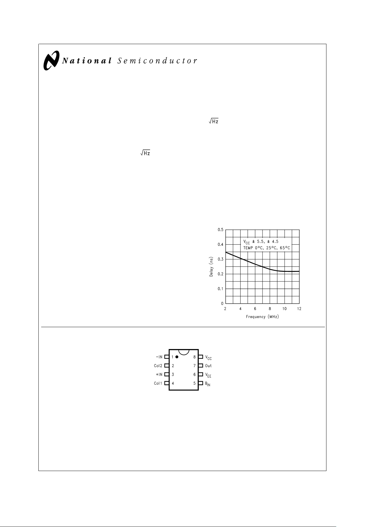
Group Delay Repeatability
DS101304-1
DS101304-3
Pinout
SOIC
January 2000
CLC5509 Ultra-Low Noise Preamplifier
© 2000 National Semiconductor Corporation DS101304 www.national.com
Page 2

Typical Application
Ordering Information
Package Temperature Range
Industrial
0˚C to 70˚C
Packaging
Marking
Transport Media NSC
Drawing
8-pin SOIC CLC5509CM CLC5509CM Rails M08A
DS101304-2
Ultrasound PreAmp
CLC5509
www.national.com 2
Page 3

Absolute Maximum Ratings (Note 1)
If Military/Aerospace specified devices are required,
please contact the National Semiconductor Sales Office/
Distributors for availability and specifications.
Supply Voltage
±
5.5V
Output Current 70mA
Common-Mode Input Voltage
±
V
CC
Maximum Junction Temperature +150˚C
Storage Temperature Range −65˚C to +150˚C
Lead Temperature (soldering 10 sec) +300˚C
ESD Rating (human body model) 4000V
Electrical Characteristics (Note 3)
(VCC,V
EE
=
±
5V, R
S
=
50Ω,A
V
=
10V/V, R
g
=
1kΩ,R
L
=
100Ω; unless specified)
Symbol Parameter Conditions Typ Min/Max
Ratings
(Note 2)
Units
Ambient Temperature CLC5509 +25˚C +25˚C
Frequency Domain Response
-3dB Bandwidth V
O
<
2.0V
PP
High Cutoff −3dB 33 28
45
MHz
Low Cutoff −3dB 0.5 0.4
0.7
MHz
Gain Flatness Inband 2
<
12.5MHz, V
O
<
1.0V
PP
−1.5
+.1
dB
Gain Accuracy
@
5MHz
±
0.3 dB
Phase Variation 3
<
9MHz, V
O
<
.1V
PP
1 Deg
Gain Variation 3
<
9MHz, V
O
<
.1V
PP
.3 dB
Time Domain Response
Rise and Fall Time 2V step 10 10
15
ns
Settling Time to 0.2
%
2V step 1 µs
Overshoot 2V step 0 5
%
Group Delay 2.5MHz
<
10MHz, V
IN
=
10mV
PP
5.5 3
7.5
ns
Group Delay Repeatability .5 ns
Distortion And Noise Response
2nd Harmonic Distortion
<
12.5MHz, V
IN
=
100mV
PP
−51 dBc
3rd Harmonic Distortion −56 dBc
Intermodulation Distortion
@
5MHz −65 dBc
Equivalent Input Noise Voltage (e
ni
)
>
1MHz, R
S
=
50Ω 0.7 0.78 nV
Noise Figure
@
50Ω 2 2.4 dB
Optimum R
S
85 80
110
Ω
Static, DC Performance
PSRR (preamp only)
<
1MHz 40 dB
Supply Current (preamp only) R
L
=
∞
911mA
Miscellaneous Performance
Output Impedance DC
<
12MHz 0.2 0.2
1
Ω
Output Voltage Range R
L
=
100Ω
±
2
±
1.7 V
Output Current
±
45
±
35 mA
CLC5509
www.national.com3
Page 4

Electrical Characteristics (Note 3) (Continued)
Note 1: “Absolute Maximum Ratings” are those values beyond which the safety of the device cannot be guaranteed. They are not meant to imply that the devices
should be operated at these limits. The table of “Electrical Characteristics” specifies conditions of device operation.
Note 2: Min/max ratings are based on product characterization and simulation. Individual parameters are tested as noted. Outgoing quality levels are determined
from tested parameters.
Note 3: All data taken in circuit shown as typical application.
Typical Performance Characteristics
Frequency Response
DS101304-4
Frequency Response
DS101304-5
Frequency Response
DS101304-6
Group Delay
DS101304-7
Group Delay
DS101304-8
3rd Harmonic Distortion
DS101304-9
CLC5509
www.national.com 4
Page 5

Typical Performance Characteristics (Continued)
3rd Harmonic Distortion
DS101304-10
2rd Harmonic Distortion
DS101304-11
2rd Harmonic Distortion
DS101304-12
Intermodulation Distortion
DS101304-13
Intermodulation Distortion
DS101304-14
Total Input Referred Noise (R
S
=
50Ω)
DS101304-15
CLC5509
www.national.com5
Page 6

Typical Performance Characteristics (Continued)
Total Input Referred Noise (R
S
=
50Ω)
DS101304-16
Total Input Referred Noise (R
S
=
100Ω)
DS101304-17
Total Input Referred Noise (R
S
=
100Ω)
DS101304-18
Total Input Referred Noise (R
S
=
200Ω)
DS101304-19
Total Input Referred Noise (R
S
=
200Ω)
DS101304-20
Z
in
DS101304-21
CLC5509
www.national.com 6
Page 7

Typical Performance Characteristics (Continued)
Z
in
DS101304-22
Z
O
DS101304-23
Z
O
DS101304-24
Positive PSRR (VCC)
DS101304-25
Positive PSRR (VCC)
DS101304-26
Negative PSRR (VEE)
DS101304-27
CLC5509
www.national.com7
Page 8

Typical Performance Characteristics (Continued)
Application Information
Introduction
The CLC5509 is a two stage ultra-low noise preamplifier,
with low distortion, and externally variable input impedance.
The unusual emitter driven input stage remains stable for a
wide range of transducer source loads. The input termination
can be matched (for 50-200Ω source matching) to a wide
range of complex loads (C
S
up to 5000pF and CPup to
10000pF, L
S
up to 1µH). The IC was designed for low cost
multiple channel ultrasound applications requiring flexible
configurations for a variety of transmit/receive topologies. In
a typical application, the CLC5509 is connected to a single
element of an ultrasound transducer through a
transmit/receive switch.
Theory of Operation
The CLC5509 simplified circuit is shown in
Figure 1
. For
analysis, the transmit/receive switch diode is modeled in the
circuit as a series resistance R
TR
with a voltage drop of VRT.
Apiezo transducer generated, single-ended voltage signal is
applied to the emitter input of the 1st stage. The voltage signal is converted to a current (i) that is passed through a high
pass filter then restored back to a voltage signal at R
g
.A high
speed, low distortion, unity gain buffer, applies the signal to
the load and feedback resistor. Negative feedback from the
buffer output to the inverting input completes the signal path.
The input and output voltage can be expressed as shown:
V
in
=
(R
TR+re
)i+VO(R1/(R1+R2))
V
O
=
−(ixR
g
) for α=1
The input resistance is calculated
The current I
BIAS1
is the input stage emitter current that
sets r
e
.
I
BIAS1
=
(V
EE-VTR
)/R
BIAS1
for V
EE
=
V
TR
=
.65V
r
e
=
26mV/I
BIAS1
Combining terms, then solving for close loop gain
V
O/Vin
results in
Negative PSRR (VEE)
DS101304-28
DS101304-29
FIGURE 1. Simplified Circuit
CLC5509
www.national.com 8
Page 9

Application Information (Continued)
Choosing External Component Values
There are three key parameters to consider in the design:
Noise, signal bandwidth, and gain. Refer to
Figure 2
.
The best noise performance for a given transmit/receive
switch R
TR
is obtained by: choosing RSbetween 50Ω and
200Ω; selecting the matching terminationresistance R
in
; and
by reducing I
BIAS1
(by increasing R
BIAS1
) to increase r
e
which optimizes the Noise Figure (NF). For this circuit, with
R
TR
=
6Ω, the optimum NF isachieved at R
s
∼ 95Ω when R
in
is set to 50Ω and Rs∼ 145Ω when Rinis set to 200Ω.
The signal bandwidth is determined by the selection of L
1
,
L
2,RBIAS1
and R
BIAS2
which set the open loop gain roll-off of
the first stage. R
g
and C2form a desirable signal path filter
that introduces an additional highpass pole. The filter values
can be chosen to create a sharper high frequency roll off of
the closed loop gain. For R
g
=
1k, C2 ∼ 470pF the small sig-
nal (V
in
<
25mW), wide bandwidth performance can be ob-
served. By increasing C
2
(to>1500pF) and increasing output series resistance with a small resistor, the stability and
harmonic distortion performance can be improved for large
signals. This filter can also be designed as a multi-pole Butterworth filter but care must be taken to ensure stability with
the desired load over the operating temperature range.
The passband gain is customer selected by setting R
g
and
R
in
. Note that using R1to reduce or increase the gain allows
for minimal interaction with other parameters.
Capacitor C
C
and resistor RCare used for local compensa-
tion of the gm input stage with values of C
C
=
0.1µF and R
C
=
1k for the applications described below.
Calculating and Measuring the Noise
The circuit input referred noise is best calculated using a
SPICE model where the external components can be optimized for the transducer source impedance and
transmit/receive switch impedance. The SPICE model for
the CLC5509 is available on the NSC web site. Refer to the
figures for total noise performance over temperature and
supply at 3mA. Once the noise is modeled and circuit parameters chosen the evaluation board can be used to measure
actual noise performance.
To measure the CLC5509 input referred noise vs. other
noise sources, several key steps should be followed. The
bench setup is fairly simple using the evaluation board and a
spectrum analyzer. (If a noise figure meter is available that is
even easier yet.) The procedure requires calibrating out the
spectrum analyzer background noise, and other noise
sources from the CLC5509 noise. Since the thermal noise of
a resistor is well known, add a series resistor R
4
between the
signal source V
in
and the L1,R
BIAS1
bias network for these
noise measurements. Several R
4
resistor values are used as
’’reference’’ noise sources. The values chosen depend on
the R
s
of the system. For R
s
=
50Ω, resistor (R
4
) with values
of 0, 12.5, 25, 50Ω should be used. If R
s
=
200Ω, resistors
(R
4
) with values of 0, 25, 50, 100, 200Ω should be used.
Start by connecting the analyzer input to the evaluation
board output. Remove R
4
from the signal source and con-
nect R
4
to GND. Now take at least 10 measurements and av-
erage them for each R
4
reference value. Be sure to divide
the result by the analyzer and circuit gain to make the noise
input referred. Subtract the R
4
=
0Ω results from the data for
each value. Compare the result to the theoretical noise values. They should agree closely over the R
s
=
0toR
in
range.
This verifies the test method.The CLC5509 noise is the R
s
=
0Ω data point. A similar procedure can be used to remove
the T/R switch noise by varying the T/R bias current I
BIAS1
.
The total circuit noise performance can now be optimized for
R
in
as described above.
Evaluation Board
Evaluation boards are available for customer product evaluation for the 8-pin SOIC. Evaluation kits that contain an
evaluation board and CLC5509 samples can be obtained by
calling National Semiconductor’s Customer Service Cen-
ter. The evaluation kit number is CLC730101. The evaluation board utilizes surface mount components. The corner
frequencies are set to ∼ 0.9MHz to 12.5MHz with a passband gain set at 20dB. The highpass filter is set at R
g
=
1k,
C
2
=
470pF to view small signal (V
in
<
25mV) performance.
Increasing C
4
(to>1500pF) reduces the bandwidth and im-
proves distortion for large signals. R
9
, is a back match resistor that terminates the output and isolates cable capacitance, for minimum distortion, over the frequency band of
interest. An R
in
∼ 50.2Ω was chosen for R
s
=
50Ω (this
source resistor R
s
is open ) and R
TR
=
0, with I
BIAS1
set to
3mA. The expected input referred noise based on bench
measurements on similar boards is ∼ 0.6nV
oraNFof
2dB. The noise can be optimized with slight variations in R
2
,
R
g
and R
BIAS1
. If transmit/receive switches are added to the
evaluation board both the voltage drop and R
TR
should be
compensated for. The R
in
, gain and noise will be affected by
the addition of the T/R switch. The V
TR
drop can be removed, to a first order, by adding a second switch in series
with the feedback gain setting resistor R
1
to ground. This will
restore the input DC level to ∼ 0V. This T/R switch diode
should be biased with a resistor (∼ R
BIAS2
)toVCCand bypassed with a 0.1µF cap to maintain the same AC performance as the evaluation board without the switches.
CLC5509 Applications
The signal path for a typical ultrasound transceiver is shown
in
Figure 3
.
DS101304-32
FIGURE 2. Complete Circuit
DS101304-33
FIGURE 3.
CLC5509
www.national.com9
Page 10

Application Information (Continued)
The CLC5509 system dynamic range performance is enhanced by using the CLC5523 variable gain amplifier as a post amplifier.
See
Figure 4
below.
The signal gain range is divided between the CLC5509 preamplifier and the post amplifier to allow wider dynamic range and better performance for high crest factor signals. There are two common ways the CLC5523 variable gain could be controlled. The
first,
Figure 5
, uses a DAC to digitally increase the gain in discrete steps. The second
Figure 6
uses anAGC loop to maintain the
maximum system input signal-to-noise. Refer to the CLC5523 data sheet applications for the implementation details.
DS101304-36
FIGURE 4. Low Noise Pre Amp with Variable Gain Amplifier Circuit
DS101304-34
FIGURE 5. VGControlled by DAC in Discrete Steps
DS101304-35
FIGURE 6. VGControlled by AGC Loop
CLC5509
www.national.com 10
Page 11

Physical Dimensions inches (millimeters) unless otherwise noted
LIFE SUPPORT POLICY
NATIONAL’S PRODUCTS ARE NOT AUTHORIZED FOR USE AS CRITICAL COMPONENTS IN LIFE SUPPORT
DEVICES OR SYSTEMS WITHOUT THE EXPRESS WRITTEN APPROVAL OF THE PRESIDENT AND GENERAL
COUNSEL OF NATIONAL SEMICONDUCTOR CORPORATION. As used herein:
1. Life support devices or systems are devices or
systems which, (a) are intended for surgical implant
into the body, or (b) support or sustain life, and
whose failure to perform when properly used in
accordance with instructions for use provided in the
labeling, can be reasonably expected to result in a
significant injury to the user.
2. A critical component is any component of a life
support device or system whose failure to perform
can be reasonably expected to cause the failure of
the life support device or system, or to affect its
safety or effectiveness.
National Semiconductor
Corporation
Americas
Tel: 1-800-272-9959
Fax: 1-800-737-7018
Email: support@nsc.com
National Semiconductor
Europe
Fax: +49 (0) 1 80-530 85 86
Email: europe.support@nsc.com
Deutsch Tel: +49 (0) 1 80-530 85 85
English Tel: +49 (0) 1 80-532 78 32
Français Tel: +49 (0) 1 80-532 93 58
Italiano Tel: +49 (0) 1 80-534 16 80
National Semiconductor
Asia Pacific Customer
Response Group
Tel: 65-2544466
Fax: 65-2504466
Email: sea.support@nsc.com
National Semiconductor
Japan Ltd.
Tel: 81-3-5639-7560
Fax: 81-3-5639-7507
www.national.com
8-pin SOIC
Order Number CLC5509CM
NS Product Number M08A
CLC5509 Ultra-Low Noise Preamplifier
National does not assume any responsibility for use of any circuitry described, no circuit patent licenses are implied and National reserves the right at any time without notice to change said circuitry and specifications.
 Loading...