

Page 1

CLC5506
Gain Trim Amplifier (GTA)
CLC5506Gain Trim Amplifier (GTA)
September 1999
General Description
The CLC5506 is a low-noise amplifier with programmable
gain for use in cellular base stations, WLL, radar and RF/IF
subsystems where gain-control is required to increase the
dynamic range. The CLC5506 allows designers to compensate for manufacturing component tolerances and temperature variations in receiver front ends. Maximum amplifier
gain is set at 26dB . A three-line MICROWIRE serial interface allows 16dB of attenuation from the max gain setting in
precise 0.25dB steps.
The CLC5506 uses a differential input and output, allowing
large outputswingson a single 5V rail. The differentialoutput
is well suited for impedance matching networks driving SAW
filters or directly driving differential input analog to digital
converters (ADC). The differential output also makes it possible to drive transformers allowing designers the ability to
match a wide variety of transmission lines. The output amplifier has excellent output drive with low distortion.
Digital control of the CLC5506 is accomplished using MICROWIRE Interface. Data Out and a Load Enable are incorporated so that more than one CLC5506/channel may be
programmed per system.
The CLC5506 maintains a 600MHz performance bandwidth
over its entire gain and attenuation range from +10dB to
+26dB. Gain control is divided into 64 equal steps of 0.25dB
and is dB-linear. Output drive and distortion performance are
excellent; In a 50Ω system, the third-order output intercept
point is +22dBm at nominal gain of 18dB at 25˚C. The
CLC5506 operates over the industrial temperature range of
−40˚C to +85˚C.
Features
n 600MHz bandwidth
n 26dB maximum gain
n 16dB gain control range
n Attenuation step size: 0.25dB
n 4.8dB noise figure
n +22dBm output IP3
n Digital ″dB Linear″ gain control
n Supply voltage: 5V
n Supply current: 75mA
n Supply shutdown: 35µA
n Package: SOIC-14
n Typical at 25˚C
@
@
26dB
@
18dB gain
150MHz
Applications
n Cellular base-stations
n Base station repeater
n Wireless Local Loop
n Radar
n Receivers
n IF amplifiers
n Digital IF receiver
n Software radio
n Satellite communications
Frequency Response vs. Gain Setting
DS101050-1
™
MICROWIRE
© 1999 National Semiconductor Corporation DS101050 www.national.com
Page 2

Typical Application
DS101050-2
www.national.com 2
Page 3

Connection Diagram
CLC5506 Pin Diagram
DS101050-3
Top View
Pin # Pin Name Description
1 NC No connection
2 GND
A
3 In+ Positive differential input
4 In− Negative differential input
5 LE MICROWIRE load enable input. High impedance CMOS input with Schmitt
6 Clock MICROWIRE clock input. High impedance CMOS input with Schmitt trigger.
7 Data In MICROWIRE data input. High impedance CMOS input with Schmitt trigger.
8 Data Out MICROWIRE data output. High impedance CMOS input with Schmitt trigger.
9 GND
10 V
D
CCD
11 Out− Negative differential Output
12 Out+ Positive differential output
13 GND
14 V
A
CCA
Analog ground
trigger
Data is clocked in on the rising edge of clock.
Binary serial data. Data entered Power Down first.
Digital ground
Digital supply voltage
Analog ground
Analog supply voltage
Ordering Information
Package
SO-14 CLC5506IM Rails M14a
Temperature Range
−40˚C to +85˚C
Transport Media NSC Drawing
CLC5506IMX 2.5k Units Tape and
Reel
CLC5506PCASM Fully loaded evaluation
board
www.national.com3
Page 4
Absolute Maximum Ratings (Note 1)
If Military/Aerospace specified devices are required,
please contact the National Semiconductor Sales Office/
Distributors for availability and specifications.
ESD tolerance(Note 2)
Human body model 2.5KV
Machine model 250V
Differential input voltage +/−1V
Supply voltage −0.3 to +6V
Digital input voltage −0.3V to V
Analog input voltage −0.3V to V
Output short circuit duration Infinite
Lead temperature (soldering, 10
sec) +300˚C
CC
CC
Storage temperature range −65˚C to 150˚C
Junction temperature 155˚C
Differential voltage between any
two inputs
<
200mV
Operating Ratings (Note 1)
Supply voltage (pins 10 and 14) 5V +/− 10
Ambient temperature range −40˚C to +85˚C
Junction Temperature Range −40˚C to +150˚C
Package thermal resistance, θ
JA
127˚C/W
%
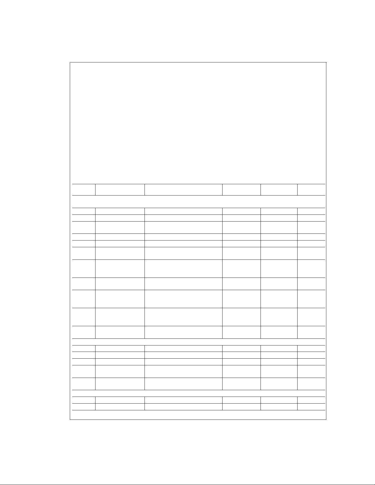
Electrical Characteristics
These conditions apply unless otherwise specified: TJ= 25˚C, V
−30dBm (Note 6),(Note 7).
Symbol Parameter Conditions
Analog I/O
Frequency Response/Distortion/Noise
upper −3dB bandwidth All Gain Codes 600 MHz
upper −1dB bandwidth All Gain Codes 400 MHz
gain flatness in any
1MHz band
group delay 50MHz
group delay ripple 50MHz
output third order
intercept point
noise figure Gain=25.75dB, (Note 6)
1dB output
compression point
nd
harmonic distortion Pin=−30 dBm, fc=200MHz
2
rd
3
harmonic distortion Pin=−30 dBm, fc=200MHz
Input/Output Isolation
power down mode
Gain Parameters: (Note 5)
maximum gain Full temperature range 25.75 dB
minimum gain Full temperature range 10 dB
gain step size Full temperature range 0.25 dB
accuracy of gain
setting
gain variation over
temperature
Input/Output Characteristics:
input resistance Differential 200 Ω
input capacitance Differential 0.5 pF
<f<
10MHz
600MHz, All Gain
Codes
<f<
600MHz 1.5 nsec
<f<
600MHz 0.5 nsec
18dB Gain, f=110MHz 22 dBm
Gain=18dB, (Note 6)
Gain=10dB, (Note 6)
150MHz 4.0 dBm
@
Gain=25.75dB
@
Gain=10dB
@
Gain=25.75dB
@
Gain=10dB
Full frequency band 45 dB
@
25˚C
Full temperature range
CCA
=
=
V
+5V: Gain=25.75dB, R
CCD
Typ
(Note 3)
Ldiff
Limit
(Note 4)
=
100Ω, Pin
=
Units
0.003 dB
4.8
5.7
7.0
46
46
49
56
±
0.05 dB
±
0.5 dB
dB
dB
dB
dBc
dBc
dBc
dBc
www.national.com 4
Page 5

Electrical Characteristics (Continued)
=
These conditions apply unless otherwise specified: TJ= 25˚C, V
−30dBm (Note 6),(Note 7).
Symbol Parameter Conditions
CCA
=
V
+5V: Gain=25.75dB, R
CCD
Typ
(Note 3)
Input/Output Characteristics:
output resistance Differential 5K Ω
output capacitance Differential 0.5 pF
Logic I/O
clock speed Maximum 1 MHz
data to clock setup
time, T
CS
data to clock hold
time, T
CH
clock pulse width high,
T
CWH
clock pulse width low,
T
CWL
clock to load enable
setup time, T
ES
high level input
voltage
low level input voltage 0.3 V
High level input
Minimum 50 nsec
Minimum 10 nsec
Minimum 50 nsec
Minimum 50 nsec
Minimum 50 nsec
0.7 V
CCD
CCD
±
1.0 µA
current
±
low level input current
high level output
voltage
low level output
Isource=0.5mA V
Isink=0.5mA 0.4 V
1.0 µA
−0.8 V
CCD
voltage
DC Characteristics:
Supply current 75 95 mA
Supply current in
35 100 µA
power down mode
Note 1: Absolute Maximum Ratings indicate limits beyond which damage to the device may occur. Operating Ratings indicate conditions for which the device is intended to be functional, but specific performance is not guaranteed. For guaranteed specifications and the test conditions, see the Electrical Characteristics.
Note 2: Human body model, 1.5kΩ in series with 100pF. Machine model, 200Ω in series with 100pF.
Note 3: Typical values represent the most likely parametric norm.
Note 4: All limits are guaranteed by testing or statistical analysis, unless otherwise noted.
Note 5: AC test performed at 400MHz unless otherwise noted.
Note 6: Refer to test circuit schematic, loss of transformers is excluded from the measurement.
Note 7: Refer to test circuit schematic to see the definition of R
Ldiff
.
Ldiff
Limit
(Note 4)
=
100Ω, Pin
Units
=
V
V
www.national.com5
Page 6

Typical Performance Characteristics (V
wise specified.)
CCA
=
=
V
+5V, R
CCD
Ldiff
=
100Ω,T
=
25˚C, unless other-
A
Frequency Response vs. Gain Setting (0.25dB/step)
DS101050-4
Gain Error vs. Input Code
DS101050-6
Input 3rd Order Intercept vs. Input Code
Gain vs. Input Code
DS101050-5
Output 3rd Order Intercept vs. Input Code
DS101050-7
Noise Figure vs. Input Code
DS101050-8
Gain Change Over Temperature vs. Frequency
DS101050-10
www.national.com 6
DS101050-9
Gain Change Over Temperature vs. Frequency
DS101050-11
Page 7

Typical Performance Characteristics (V
otherwise specified.)) (Continued)
CCA
=
=
V
+5V, R
CCD
Ldiff
=
100Ω,T
=
25˚C, unless
A
Gain Change Over Temperature vs. Frequency
DS101050-12
NF Change Over Temperature vs. Frequency
DS101050-14
P
vs. Gain Setting
1dB
NF Change Over Temperature vs. Frequency
DS101050-13
NF Change Over Temperature vs. Frequency
DS101050-15
DS101050-16
www.national.com7
Page 8

FIGURE 1. CLC5506 Functional Block Diagram
APPLICATION NOTE
Description
Figure 1
gram overview.
The LNA(Low NoiseAmplifier) is responsible for maintaining
a nominal input impedance of 200Ω with minimum noise
contribution and some finite and fixed amount of gain (∼4).
Exceptional Noise Figure (NF) performance of 4.8dB (
Gain = 25.75dB) is achieved by utilizing an active impedance
matching circuit technique which overcomes the inevitable
3dB NF penalty when using passive shunt matching.
The LNA stage is immediately followed by a transconductance stage (Gm) which thenconverts the LNA’s voltage output into a differential current output with fixed gain.
The 6-bit D/A converter, which processes the digital code
read into the device using the MICROWIRE interface, consists of a 6-bit R2R ladder. In order to achieve true ″Linear in
dB″ gain control at the output, the D/A converter output is
processed by a ″Linear to Exponential″ converter block be-
Power Down
The CLC5506 is able to go to a Power Down mode in order
to minimize its power consumption to a fraction of its nominal
value. The Power Down mode is activated through the MICROWIRE interface by clocking in a ″1″ into the Power
Down shift register prior to allowing LE (pin 5) to go high. Refer to
above shows the CLC5506 functional block dia-
Gain Typical Gain Setting (dB) Note
0 10 Minimum Gain Setting
1 10.25
2 10.5
*** ***
K 10 + 0.25
*
K
*** ***
62 25.50
63 25.75 Maximum Gain Setting
Figure 2
and
Figure 3
for more information.
DS101050-17
fore being used to set the gain of the input signal. The ″Linear to Exponential″ block and the ″Temperature Compensation″ blocks work in conjunction to achieve gain stability over
the temperature range. Finally, the output stage consists of a
variable gain cell with open Collector output. This variable
gain cell sets the signal channel gain in accordance with the
value of the digital code.
@
Gain Control
The CLC5506 minimum gain is at 10dB nominal. There are
a total of 64 distinct gain control codes possible (serial data
input through Data In pin) at 0.25dB/code resulting in a maximum nominal gain of 25.75dB.
Therefore, the overall gain can be written as:
Gain (dB) = 10dB + N
where N
code
control code.
refers to the decimal equivalent of the 6-bit gain
* 0.25 (dB/code)
code
TABLE 1.
In Power Down mode, the CLC5506 sinks less than 35µA.
The CLC5506 will wake up to the requested gain level specified by Data In through the MICROWIRE interface.
When V
it would always ″wake up″ with a nominal gain of 17.75dB
(N
is first applied, the device is configured such that
CC
=
3).
code
www.national.com 8
Page 9

APPLICATION NOTE (Continued)
MICROWIRE
Data In along with the Clock, LE, and Data Out, is used for
the following purposes:
mize power consumption
terface devices through the Data Out pin
The MICROWIRE interface timing diagram along with the bit
assignment of all 8 bits is shown in
active only when LE (pin 5) is low; otherwise, the interface is
inactive (Clock and Data In are ignored) and the CLC5506
gain is the current content of the 6 bits already read into the
device.
1. Data is clocked in on the rising edge of Clock.
2. Power Down bit is the first data to enter the CLC5506.
™
Interface
Setting the 6-bit gain control code
Putting the device into a Power Up/Down mode to mini-
Daisy chain several CLC5506 or other MICROWIRE In-
Figure 2
. The interface is
FIGURE 2. MICROWIRE Interface Timing Diagram
With LE low,each successive positive transition of Clock will
read the value of the Data In into a series of 8 single bit shift
registers. In order to load all 8 registers, 8 Clock transitions
are required after which, when LE is allowed to go High, the
new values in the shift registers are latched to determine the
device gain setting (or Power Down state). New data can be
shifted into the device with the present gain setting not affected as long as LE is held low.
Data from the last register in the chain is clocked out on Data
Out pin on the negative transitions of Clock as shown in
ure 3
. This enables several MICROWIRE Interface devices
Fig-
to be daisy chained and controlled from a single bus master.
The maximum clock frequency (Clock pin) is 1MHz.
DS101050-18
Note:
FIGURE 3. MICROWIRE Interface Serial Data Out Timing
DS101050-19
www.national.com9
Page 10

APPLICATION NOTE (Continued)
Differential Input and Output Considerations
The CLC5506 typical application requires DC blocking capacitors for both inputs and outputs to main internal DC biasing points.
The input impedance between the differential inputs (IN+,
IN-) is 200Ω//0.5pF. Since the 0.5pF capacitance can be neglected in the VHF band, a 1:4 impedance ratio balun can be
used to transform a 50Ω source to the 200Ω differential inputs of CLC5506 for wide band design.
The CLC5506 has a pair of open collector differential outputs
(OUT+, OUT-).DC biasing is achieved through an RF inductor.The RFinductor acts asa choke toblock RF leakage and
interference. An external resistor across the differential out-
FIGURE 4. Narrow band design example with balanced SAW filter and ADC
CLC5506 Evaluation Board
A proper printed circuit layout is essential for achieving high
frequency performance. To expedite evaluation, an assembled and tested evaluation kit CLC5506PCASM is available for sale. See application note AN-1138for technical details of evaluation kit. Order information and application note
is available on the Web at http://www.national.com
puts is used to set the output resistance of CLC5506. Wideband output matching to an unbalanced 50Ω load can be
achieved by using a 1:n balun. A 1:4 impedance ratio balun
is used when a 200Ω external resistor is used in a 50Ω system.
Although the CLC5506 can be used as a single-ended device by grounding one of the inputs through a capacitor, the
noise figure would be severely degraded by 6dB.
The CLC5506 can also directly interface to balanced devices, like SAW filters and ADCs. Narrowband design example with ADC CLC5956 and SAW filter is provided below.
The component values of matching inductors and capacitors
depend on the actual input/output impedance of the SAW filter, ADC, PWB properties, layout and frequency band.
DS101050-20
www.national.com 10
Page 11

CLC5506 Test Circuit Schematic
DS101050-21
www.national.com11
Page 12

Physical Dimensions inches (millimeters) unless otherwise noted
CLC5506Gain Trim Amplifier (GTA)
14-Pin Small Outline
NSC Package Number M14A
LIFE SUPPORT POLICY
NATIONAL’S PRODUCTS ARE NOT AUTHORIZED FOR USE AS CRITICAL COMPONENTS IN LIFE SUPPORT
DEVICES OR SYSTEMS WITHOUT THE EXPRESS WRITTEN APPROVAL OF THE PRESIDENT AND GENERAL
COUNSEL OF NATIONAL SEMICONDUCTOR CORPORATION. As used herein:
1. Life support devices or systems are devices or
systems which, (a) are intended for surgical implant
into the body, or (b) support or sustain life, and
whose failure to perform when properly used in
accordance with instructions for use provided in the
2. A critical component is any component of a life
support device or system whose failure to perform
can be reasonably expected to cause the failure of
the life support device or system, or to affect its
safety or effectiveness.
labeling, can be reasonably expected to result in a
significant injury to the user.
National Semiconductor
Corporation
Americas
Tel: 1-800-272-9959
Fax: 1-800-737-7018
Email: support@nsc.com
www.national.com
National does not assume any responsibility for use of any circuitry described, no circuit patent licenses are implied and National reserves the right at any time without notice to change said circuitry and specifications.
National Semiconductor
Europe
Fax: +49 (0) 1 80-530 85 86
Email: europe.support@nsc.com
Deutsch Tel: +49 (0) 1 80-530 85 85
English Tel: +49 (0) 1 80-532 78 32
Français Tel: +49 (0) 1 80-532 93 58
Italiano Tel: +49 (0) 1 80-534 16 80
National Semiconductor
Asia Pacific Customer
Response Group
Tel: 65-2544466
Fax: 65-2504466
Email: sea.support@nsc.com
National Semiconductor
Japan Ltd.
Tel: 81-3-5639-7560
Fax: 81-3-5639-7507
 Loading...