

Datasheet CLC533MDC, CLC533AJP, CLC533AJE-TR13, CLC533AJE, 5962-9320301MEA Datasheet (NSC)
...Page 1
Features
■
12-bit settling (0.01%) – 17ns
■
Low noise – 42µVrms
■
Isolation – 80dB @ 10MHz
■
110MHz -3dB bandwidth (Av= +2)
■
Low distortion – 80dB @ 5MHz
■
Adjustable bandwidth – 180MHz (max)
Applications
■
Infrared system multiplexing
■
CCD sensor signals
■
Radar I/Q switching
■
High definition video HDTV
■
Test and calibration
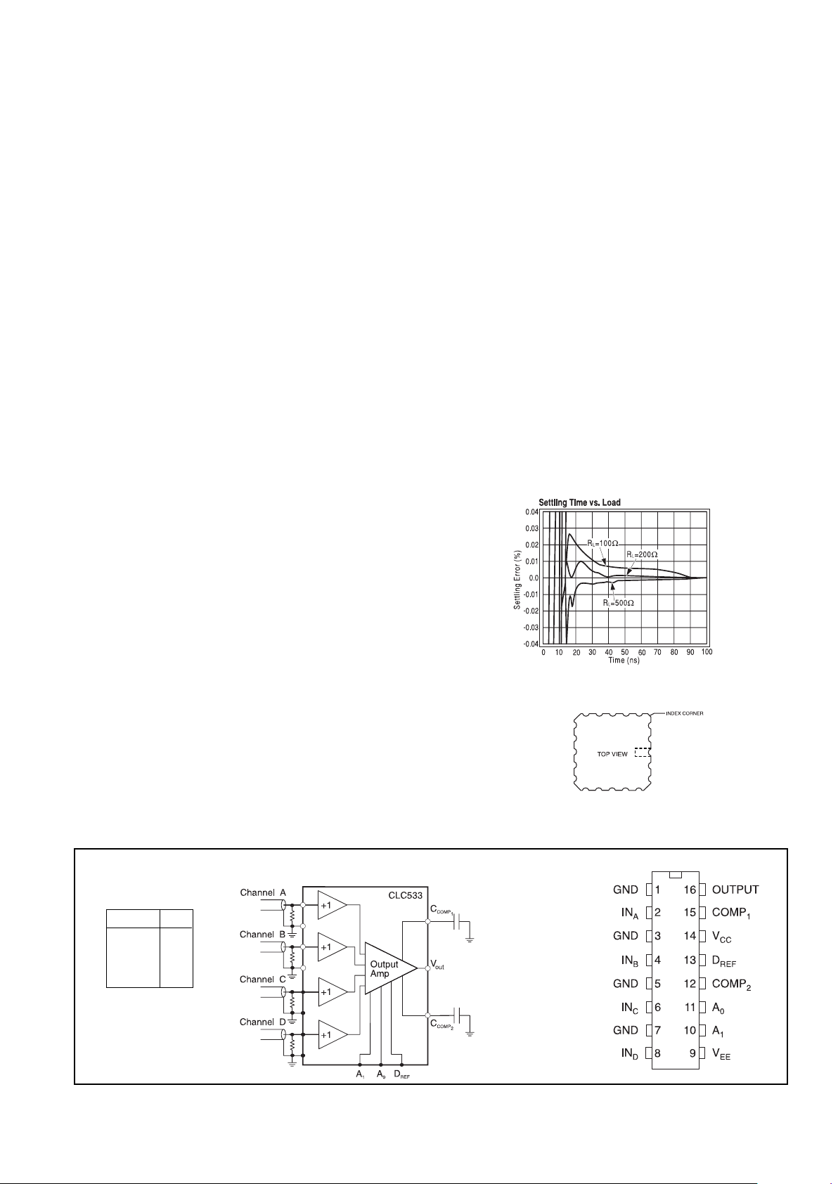
Functional Diagram
Pinout
DIP & SOIC
General Description
The CLC533 is a high-speed 4:1 multiplexer employing active
input and output stages. The CLC533 also employs a closed-loop
design which dramatically improves accuracy over conventional
analog multiplexer circuits. This monolithic device is constructed
using an advanced high-performance bipolar process.
The CLC533 has been specifically designed to provide a 24ns
settling time to 0.01%. This coupled with the adjustable bandwidth, makes the CLC533 an ideal choice for infrared and CCD
imaging systems, with channel-to-channel isolation of 80dB @
10MHz. Low distortion and spurious signal levels (-80dBc) make
the CLC533 a very suitable choice for I/Q processors in radar
receivers.
The CLC533 is offered over both the industrial and militar y temperature ranges. The industrial versions, CLC533AJP\AJE\AIB,
are specified from -40°C to +85°C and are packaged in 16-pin
plastic DIPs, SOIC’s and CERDIP packages. The extended temperature versions, CLC533A8B/A8L-2A, are specified from -55°C
to +125°C and are packaged in 16-pin CERDIP and 20-terminal
LCC packages.
Ordering Information ...
CLC533AJP -40°C to +85°C 16-pin plastic DIP
CLC533AJE -40°C to +85°C 16-pin plastic SOIC
CLC533ALC -40°C to +85°C dice
CLC533A8B -55°C to +125°C 16-pin CERDIP,
MIL-STD-883
CLC533AMC -40°C to +85°C dice, MIL-STD-833
CLC533A8L-2A -55°C to +125°C 20-ter minal LCC,
MIL-STD-883
Contact factory for other packages and DESC SMD number.
CLC533
High-Speed 4:1 Analog Multiplexer
N
June 1999
CLC533
High-Speed 4:1 Analog Multiplexer
A1A0OUT
00 A
01 B
10 C
11 D
ECL Mode - D
REF
= open
TTL Mode - D
REF
= +5V
INA3
GND2
NC1
OUTPUT20
COMP
1
19
GND 9
IN
D
10
NC 11
V
ee
12
A
1
13
14
A
0
15
COMP
2
16NC17
D
REF
18
V
cc
8
GND
7
IN
B
6NC5
GND
4
IN
c
© 1999 National Semiconductor Corporation http://www.national.com
Printed in the U.S.A.
Page 2
http://www.national.com 2
PARAMETERS CONDITIONS TYP MIN/MAX RATINGS
2
UNITS SYMBOL
Ambient T emper ature CLC533AJP/AJE/AIB +25°C -40°C +25°C +85°C
FREQUENCY DOMAIN RESPONSE
-3dB bandwidth V
OUT
< 0.1V
pp
180 130 130 110 MHz SSBW
-3dB bandwidth V
OUT
= 2V
pp
45 35 35 30 MHz LSBW
gain flatness V
OUT
< 0.1V
pp
peaking 0.1MHz to 200MHz 0.2 0.5 0.5 0.5 dB GFP
rolloff 0.1MHz to 100MHz 1.0 2.0 2.0 3.0 dB GFR
linear phase deviation dc to 100MHz 2.0 deg LPD
crosstalk rejection - 1 channel 2V
pp
, 10MHz 80 74 74 74 dB CT10
2V
pp
, 20MHz 74 68 68 68 dB CT20
2V
pp
, 30MHz 68 62 62 62 dB CT30
crosstalk rejection - 3 channels 2V
pp
, 10MHz 80 74 74 74 dB 3CT10
2V
pp
, 20MHz 74 68 68 68 dB 3CT20
2V
pp
, 30MHz 68 62 62 62 dB 3CT30
TIME DOMAIN PERFORMANCE
rise and fall time 0.5V step 2.7 3.3 3.3 3.8 ns TRS
2V step 10 12.5 12.5 14.5 ns TRL
settling time
2
2V step ±0.01% 17 24 24 27 ns TSP
±0.1% 13 18 18 21 ns TSS
overshoot 2.0V step 2 5 5 6 % OS
slew rate 160 130 130 110 V/µsSR
SWITCH PERFORMANCE
channel to channel switching time 50% SELECT to 10%V
OUT
6 8 8 9 ns SWT10
(2V step at output) 50% SELECT to 90%V
OUT
16 21 21 24 ns SWT90
switching transient 30 mV ST
DISTORTION AND NOISE PERFORMANCE
2nd harmonic distortion 2V
pp
, 5MHz 80 67 67 67 dBc HD2
3rd harmonic distortion 2V
pp
, 5MHz 86 67 67 67 dBc HD3
equivalent input noise
spot noise voltage > 1MHz 4.2 nV/√Hz SNF
integrated noise 1MHz to 100MHz 42 54 51 mVrms INV
spot noise current 5 pA/√Hz SNF
STATIC AND DC PERFORMANCE
* analog output offset 1 12 3.5 4.5 mV VOS
temperature coefficient 15 90 20 µV/°C D VIO
* analog input bias current 50 280 120 120 µA IBN
temperature coefficient 0.3 2.0 0.8 µA/°C DIBN
analog input resistance 200 90 120 120 kΩ RIN
analog input capacitance 2 3.0 2.5 2.5 pF CIN
* gain accuracy ±2V 0.994 0.988 0.988 0.988 V/V GA
integral endpoint linearity ±1V (full scale) 0.02 0.05 0.03 0.03 %FS ILIN
output voltage no load ±3.4 2.4 2.8 2.8 V VO
output current 45 20 50 50 mA IO
output resistance DC 1.5 4.0 2.5 2.5 Ω RO
DIGITAL INPUT PERFORMANCE
ECL mode (D
REF
floating)
input voltage logic HIGH -1.1 -1.1 -1.1 V VIH1
input voltage logic LOW -1.5 -1.5 -1.5 V VIL1
input current logic HIGH 200 220 80 80 µA IIH1
input current logic LOW 200 220 80 80 µA IIL1
TTL mode (D
REF
= +5V)
input voltage logic HIGH 2.0 2.0 2.0 V VIH2
input voltage logic LOW 0.8 0.8 0.8 V VIL2
input current logic HIGH 200 220 80 80 µA IIH2
input current logic LOW 200 220 80 80 µA IIL2
POWER REQUIREMENTS
* supply current (+V
CC
= +5.0V) no load 28 38 36 36 mA ICC
* supply current (-V
ee
= -5.2V) no load 28.5 39 37 37 mA IEE
nominal power dissipation no load 288 mW PD
* power supply rejection ratio -53 -60 -60 dB PSRR
Min/max ratings are based on product characterization and simulation. Individual parameters are tested as noted. Outgoing quality levels are
determined from tested parameters.
CLC533 Electrical Characteristics
(+Vcc= +5.0V; -Vee= -5.2V; Rin= 50Ω;RL= 500Ω;C
COMP
= 8pf; ECL Mode, pin 13 = NC)
Page 3
3 http://www.national.com
Small Signal Gain/Phase vs. Load*
*with recommended C
COMP
Digitalized Pulse Response
±
±
CLC533 Typical Performance Characteristics
(TA = 25°C, +Vcc = +5V, -Vee = -5.2V, RL = 500Ω unless specified)
Page 4

http://www.national.com 4
CLC533 Typical Performance Characteristics
(TA = 25°C, +Vcc = +5V, -Vee = -5.2V, RL = 500Ω unless specified)
Page 5

5 http://www.national.com
positive supply voltage (+Vcc) +5.0V
negative supply voltage (-Vee) -5.2V
differential voltage between any two GND’s 10mV
analog input voltage range ±2V
AXinput voltage range (TTL mode) 0V to +5.0V
AXinput voltage range (ECL mode) 0V to -2.0V
C
COMP
range 5pF to 100pF
thermal data θjc(°C/W) θja(°C/W)
16-pin plastic 50 60
16-pin Cerdip 20 65
16-pin SOIC 60 75
20-terminal LCC 20 35
16-pin side brazed 20 50
positive supply voltage (+Vcc) -0.5V to +7.0V
negative supply voltage (-Vee) +0.5V to -7.0V
differential voltage between any two GND’s 200mV
analog input voltage range -Veeto +V
cc
digital input voltage range -Veeto +V
cc
output short circuit duration (shorted to GND) Infinite
junction temperature +150°C
operating temperature range
CLC533AJP/AJE/AIB -40°C to +85°C
storage temperature range -65°C to +150°C
lead solder duration (+300°C) 10 sec
ESD rating (human body model) <500V
Recommended Operating Conditions Absolute Maximum Ratings
3
Note 1: Test levels are as follows:
* AJ : 100% tested at +25°C.
Note 2: Settling time measured from the 50% analog output
transition.
Note 3: Absolute maximum ratings are limiting values, to be
applied individually , and bey ond which the serviceability of the cir-
cuit may be impaired. Functional operability under any of these
conditions is not necessarily implied. Exposure to maximum ratings for extended periods may affect device reliability.
System Timing Diagram Switching T ransient Timing Diagram
APPLICATIONS INFORMATION
Operation
The CLC533 is a 4:1 analog multiplexer designed with a
closed loop architecture to provide very low harmonic
distortion and superior channel to channel isolation. This
low distortion, coupled with very fast switching
speed make the CLC533 an ideal multiplexer for data
conversion applications. User selectable ECL or TTL
select logic adds to the versatility of this device . External
frequency response compensation allows the
performance of the CLC533 to be optimized for each
application.
Digital Interface and Channel Select
The CLC533 has two channel select pins which can be
used to select any one of the four inputs. These
digital inputs can be configured to meet TTL, ECL or
CMOS logic levels with the D
REF
pin. If D
REF
is left
open, then the A0and A1select inputs will respond to
ECL 10K switching levels (Figure 1). For TTL or CMOS
levels, D
REF
should be tied to V
cc
(Figure 2). There is an
internal series resistor which makes it possible to
connect D
REF
directly to the power supply. Select pins
according to the truth table shown on the front page. A
more positive voltage is considered to be a logic ‘1’.
Therefore with no connection to A0or A1the internal pullup resistors will select the D input to be passed through
to the output.
Compensation
The CLC533 is externally compensated, allowing
the user to select the bandwidth that best suits
the application. Decreasing bandwidth has two
advantages: lower noise and lower switching transients. In a sampled system, noise at frequencies
Pac kage Thermal Resistance
Package θ
JC
θ
JA
AJP 45°C/W 95°C/W
AJE 35°C/W 100°C/W
CERDIP 25°C/W 65°C/W
Reliability Information
Transistor count 144
Page 6

http://www.national.com 6
above 1/2 the sampling frequency will be aliased into
the baseband and will corrupt the signal of interest.
When the CLC533 is switched from one channel to
another, the output slews rapidly until it arrives at
the new signal. This high slew rate signal can capacitively couple into other nodes in the circuit and can
have a detrimental effect on overall performance.
Since coupling through stray capacitance and
inductances decreases with decreasing dV/dt, the
slew rate should be minimized consistent with system
throughput requirements.
Figure 1: ECL Level Channel SELECT Configuration
Figure 2:TTL/CMOS Level Channel
SELECT Configuration
Output Load
The final frequency response that is realized is a result of
both the compensation capacitor and the load that the
CLC533 is driving. Figure 3 below shows the effect that
C
COMP
has on bandwidth for a fixed load. Graphs on the
preceding pages demonstrate the effect of C
COMP
on
pulse response and settling time, and the optimum value
of C
COMP
to maximize bandwidth for various amounts of
resistive loading. Because there are so many factors that
go into determining the optimum value of C
COMP
it is
recommended that once a value is selected, the
application circuit be built up and larger and smaller
compensation capacitors be tried to determine the best
value for that particular circuit.
The output load that the CLC533 is driving has an effect
on the harmonic distortion of the device as well as
frequency response. Distortion is minimized with a 500Ω
load. When driving components with a high input
impedance, addition of a load resistor can improve the
performance. If the load is capacitive in nature, it should
be isolated from the CLC533 output via a series resistor.
The recommended series resistor Rs, for various
capacitive loads CL, can be found by referring to the
“Recommended Compensation Cap vs. Load” plot in the
“Typical Performance” section.
Figure 3
Power Supplies and Grounding
In any circuit there are connections between
components that are not desired. Some of the most common of these are the connections made through the
power supply and grounding network. The goal in laying
out the power and ground network for a mixed mode
circuit is to minimize the impedance from the power pins
to the supply, and minimize the impedance of the ground
network.
To minimize impedance of the ground and power nets,
use the heaviest possible traces and ground planes for
minimizing the DC impedance. To further reduce the
supply impedance at higher frequencies, a 6 to 10µF
capacitor should be placed between supply lines and
ground. At very high frequencies, the inductance in the
traces becomes significant and 0.01 to 0.1µF bypass
capacitors need to be placed as close to each power pin
as is practical. To reduce the negative effects of ground
impedances that will exist, consider the paths that ground
currents must take to get from the various devices on the
circuit card to the power supply. To achieve good system
performance, i t i s vital that large currents and high-speed
time varying currents like CMOS signals, be kept away
from precision analog components. This can be achieved
through layout of the power and ground nets. Using a
ground plane split between analog and digital sections of
the circuit forces all of the ground current from the digital
circuits to go directly to the power connector without
straying to the analog side of the card.
Optimizing for Channel-to-Channel Isolation
Although the CLC533 has excellent channel-tochannel isolation, if there is cross talk between the input
signals before they reach the CLC533, the
multiplexer will faithfully pass these corrupted signals
through to its output and dutifully take the blame for poor
Small Signal Bandwidth (30MHz/div)
50Ω 50Ω
81Ω
130Ω
Page 7

7 http://www.national.com
isolation. The CLC533 evaluation board has
successfully demonstrated in excess of 80dB of
isolation and can be considered to be a model for the
layout of boards requiring good isolation. The evaluation
board has input signal traces shielded by a guard ring as
shown in Figure 4. These guard rings help to
prevent ground return currents from other channels finding their way into the selected channel. If there are input
termination resistors, care must be taken that the ground
return currents between resistors cannot interfere with
each other. Use of chip resistors allows for best isolation, and if the guard ring around the input trace is used
for the termination resistor ground, then the ground
currents for each input are forced to tak e paths aw a y from
one another.
Figure 4: Analog Input Using Guard Ring
Use of the CLC533 with an Analog-to-Digital Converter
To get the most out of the combination of multiplexer and
ADC, a clear understanding of both conver ter operation
and multiplex er operation is required. Careful attention to
the timing of the convert signal to the ADC and the channel select signal to the CLC533 is one key to
optimizing performance.
To obtain the best performance from the combination, the
output of the CLC533 must be a valid representation of the
selected input at the time that the ADC samples it. The
time at which the ADC samples the input is determined
by the type of ADC that is being used.Subranging ADCs
usually have a Track-and-Hold (T/H) at their input. For a
successful combination of the multiplexer and the ADC,
the multiplexer timing and the T/H timing must be compatible.When the ADC is given a convert command, the T/H
transitions from Track mode to Hold mode. The delay
between the convert command and this transition is
usually specified as Aperture Delay or as Sampling Time
Offset. To maximize the time that the multiplexer has to
settle and the T/H has to acquire the signal, the multiplexer should begin its transition from one input to the
other immediately after the T/H transition has taken
place. However it is during this per iod of time that a subranging ADC is performing analog processing of the
sampled signal, and high slew rate transitions on the
input may feed through to the sample being converted.
To minimize this interaction there are two strategies that
can be taken: strategy one applies when the sample rate
of the system is below the rated speed of the conver ter.
Here the select timing is delayed so that the multiplexer
transition takes place after the A/D has completed one
conversion cycle and is waiting for the next convert
command. As an example: a CLC935 (15Msps) A/D
converter is being used at 10 MHz, the conversion takes
place in the first 67ns after the convert command, the
next 33ns are spent waiting for the next convert
command and would be an ideal time to transition the
multiplexer from one channel to the next. The second
optimization strategy involves lowering the analog input
slew rate so that it has fewer high frequency components
that might feed through to the hold capacitor while the
converter’s T/H is in hold mode. This slew rate limitation
can be done through the use of the external CLC533
compensation capacitors. Use of this method has the
advantage of limiting some of the excess bandwidth that
the CLC533 has compared to the ADC. This bandwidth
limitation will reduce the amount of high frequency noise
that is aliased back into the sampled band. Figure 5
shows recommended C
COMP
values that can be used as
a function of ADC Sample rate. Since the optimal values
will change from one ADC to the next, this graph should
be used as a starting point for C
COMP
selection.
Figure 5
Flash ADCs are similar to subranging ADCs in that the
sampling period is very brief. The primary difference is
that the acquisition time of a flash converter is much
shorter than that of a subranging A/D. With a flash ADC
the transition of the mux output should be after the
sampling instant (Aperture delay after the convert
command). The periods of time during which the
internal circuitry in a flash converter is sensitive to
external disruptions are relatively brief. It is only
during these points in time that the converter is
susceptible to interference from the input. It may be
found that a slight delay between the ADC clock and the
CLC533 select lines will have a positive effect on overall
performance.
Channel A
Connector
Channel B
Connector
Pin 1
Chip Resistors
Ground Ring
Recommended C
COMP
vs. ADC Sample Rate
Sample Rate (MHz)
C
COMP
(pF)
10 12 14 16 18 20
50
40
30
20
10
Page 8

Mixed Mode Circuit Design
In any mixed mode circuit care must be tak en to k eep the
high slew-rate digital signals from interfering with the high
precision analog signals. A successful design will take
this into consideration from many angles and will account
for it in digital timing, logic family selected, PCB layout,
analog signal bandwidth and a myriad of other aspects.
Below are a few tips that should be kept in mind when
designing a circuit that involves both analog and digital
circuitry.
Timing
If the analog signals going through the CLC533 are to be
sampled, try to minimize the amount of digital logic
switching concurrent with the sampling instant.
Power Supply Net
In an analog system the ideal situation would have each
circuit element completely isolated from all others except
for the intended connections. One of the most common
ways f or unwanted connections to be made is through the
power supplies and ground. These are often shared by
all of the circuits in the system. Refer to the section on
power supplies and grounding for tips on how to a v oid these
pitfalls.
Logic Family Selection
When designing digital logic, there are often sev eral logic
families that will provide a solution to the problem at
hand. Although they may perform equally in a
digital sense, they may have varying degrees of
influence on the analog circuits in the same system.
Coupling of digital signals with analog signals through
stray capacitances is rarely a problem for the digital logic
but can be a detrimental to an otherwise good analog
design. To minimize coupling, lay out the board to
minimize the stray capacitances as much as
possible: if an analog and a digital signal must cross,
make them cross at right angles and avoid long
parallel runs. If a 74LS00 will work in a socket, using a
74F00 will probably have no effect on the digital
circuitry, but the faster edges will find it easier to
corrupt analog signals. When faced with a choice
between several logic families, select the slowest one
possible to get the job done. Don’t forget that the slew
rates of digital logic depend not only on the rise and fall
times, but on the output swing as well. ECL gates with a
1ns rise time have much slower slew rates than TTL
gates with the same rise times. Do not attempt to slow
logic edge rates through the addition of capacitance on
the logic lines.
The negative effects that digital logic has on po wer supplies
is not constant through different logic families. CMOS
logic draws current only during transitions. The surge
currents that it draws at these times can be quite significant
and can be very disruptive to the power and ground networks. ECL tends to draw constant amounts of current
and has a much smaller effect on the power net.
Gain Selection for an ADC
In many applications, such as RADAR, the dynamic
range requirements may exceed the accuracy
requirements. Since wide dynamic range ADCs are also
typically highly accurate ADCs this often leads the
designer into an ADC which is a technical overkill and a
budget buster . By using the CLC533 as a selectable gain
stage, a less expensive A/D can be used. For example, if
an application calls for 85dB of dynamic range and 0.05%
accuracy, rather than using a 16 bit converter, use a 12
bit converter with the circuit shown below. In this circuit
the CLC533 is used to select between the input signal
and version of the input signal attenuated by 6, 12 and
18dB. This circuit affords better than 14 bit dynamic
range, 12 bit accuracy and a 12 bit price. By using
resistors of all the same value, a single resistor network
can be used which can assure good matching of the
resistors, even over temperature.
Figure 6
Evaluation Board
Evaluation boards are available for both the DIP
versions (Part number CLC730035) and SOIC version
(part number CLC730039) of the CLC533. These boards
can be used for fast, trouble free evaluation and characterization of the CLC533. Additionally this board serves
an example of a successful PCB layout that can be
copied into applications circuits. A separate data sheet
for the evaluation board can be obtained.
V
in
CLC533
R
R
R
R R
R
R
R
V
out
Gain Select
A
1
A
0
AB
C
D
http://www.national.com 8
Page 9

CLC533
High-Speed 4:1 Analog Multiplexer
http://www.national.com 9
Customer Design Applications Support
National Semiconductor is committed to design excellence. For sales, literature and technical support, call the
National Semiconductor Customer Response Group at 1-800-272-9959 or fax 1-800-737-7018.
Life Support Policy
National’s products are not authorized for use as critical components in life support devices or systems without the express written approval of
the president of National Semiconductor Corporation. As used herein:
1. Life support devices or systems are devices or systems which, a) are intended for surgical implant into the body, or b) support or
sustain life, and whose failure to perform, when proper ly used in accordance with instructions for use provided in the labeling, can
be reasonably expected to result in a significant injury to the user.
2. A critical component is any component of a life support device or system whose failure to perform can be reasonably expected to
cause the failure of the life support device or system, or to affect its safety or effectiveness.
National Semiconductor National Semiconductor National Semiconductor National Semiconductor
Corporation Europe Hong Kong Ltd. Japan Ltd.
1111 West Bardin Road Fax:(+49) 0-180-530 85 86 2501 Miramar Tower Tel: 81-043-299-2309
Arlington, TX 76017 E-mail: europe.suppor t.nsc.com 1-23 Kimberley Road Fax:81-043-299-2408
Tel: 1(800) 272-9959 Deutsch Tel:(+49) 0-180-530 85 85 Tsimshatsui, Kowloon
Fax:1(800) 737-7018 English Tel:(+49) 0-180-532 78 32 Hong Kong
Francais Tel:(+49) 0-180-532 93 58 Tel: (852) 2737-1600
Italiano Tel: (+49) 0-180-534 16 80 Fax: (852) 2736-9960
National does not assume any responsibility for use of any circuitry described, no circuit patent licenses are implied and National reserves the right at any time without notice to change said
circuitry and specifications.
N
 Loading...