

Page 1
N
CLC522
Wideband Variable-Gain Amplifier
General Description
The CLC522 variable gain amplifier (VGA) is a dc-coupled, twoquadrant multiplier with differential voltage inputs and a single-ended
voltage output. Two input buffers and an output operational amplifer
are integrated with the multiplier core to make the CLC522 a complete
VGA system that does not require external buffering.
The CLC522 provides the flexibility of externally setting the maximum
gain with only two external resistors. Greater than 40dB gain control
is easily achieved through a single high impedance voltage input. The
CLC522 provides a linear (in Volts per Volt) relationship between the
amplifier's gain and the gain-control input voltage.
The CLC522's maximum gain may be set anywhere over a nominal
range of 2V/V to 100V/V. The gain control input then provides
attenuation from the maximum setting. For example, set for a
maximum gain of 100V/V, the CLC522 will provide a 100V/V to 1V/V
gain control range by sweeping the gain control input voltage from +1
to -0.98V.
Set at a maximum gain of 10V/V, the CLC522 provides a 165MHz
signal channel bandwidth and a 165MHz gain control bandwidth. Gain
nonlinearity over a 40dB gain range is 0.5% and gain accuracy at
A
V
max
= 10V/V is typically ±0.3%.
June 1999
CLC522
Wideband V ariable-Gain Amplifier
Features
■ 330MHz signal bandwidth: A
vmax
= 2
■ 165MHz gain-control bandwidth
■ 0.3° to 60MHz linear phase deviation
■ 0.04% (-68dB) signal-channel non-linearity
■ >40dB gain-adjustment range
■ Differential or single-end voltage inputs
■ Single-ended voltage output
Applications
■ Variable attenuators
■ Pulse amplitude equalizers
■ HF modulators
■ Automatic gain control & leveling loops
■ Video production switching
■ Differential line receivers
■ Voltage controlled filters
1999 National Semiconductor Corporation http://www.national.com
Printed in the U.S.A.
Gain (V/V)
Gain vs. Gain Control Voltage (Vg)
-1.1
Gain Control Voltage, V
g
(Volts)
1.1
10
0
V
Vn
s
CR
ss
CRkCR
k
R
R
Q
k
R
R
k
CR
o
in
b
by
f
g
b
y
o
y
=−
++
===
1
1
1
185
2
2
2
., ,
ω
TT
TT
T
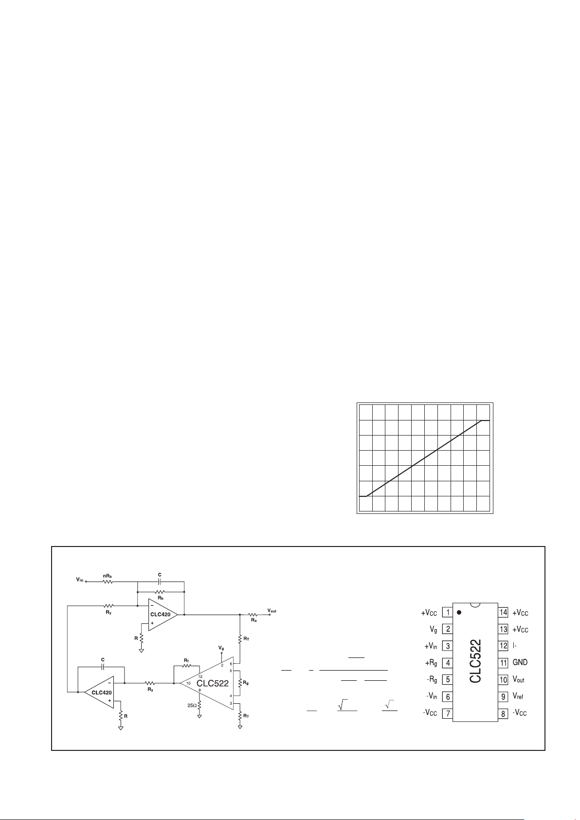
ypical Applicationypical Application
ypical Applicationypical Application
ypical Application
2nd Order Tuneable Bandpass Filter
Pinout
DIP & SOIC
Page 2
CLC522 Electrical Characteristics
(V
CC
= ±5V; A
Vmax
= +10; R
f
=1k
ΩΩ
ΩΩ
Ω; R
g
=182W; R
L
= 100
ΩΩ
ΩΩ
Ω; Vg=+1.1V)
Ordering Information
supply voltage ±7V
short circuit current 80mA
common-mode input voltage ±V
cc
maximum junction temperature +150°C
storage temperature -65°C to+150°C
lead temperature (soldering 10 sec) +300°C
transistor count 74
Absolute Maximum Ratings
Notes
1) AJE (SOIC) is tested/guaranteed with Rf=866Ω and Rg= 165Ω.
2) J-level, spec is 100% tested at +25°C.
3) Specified with Vin = 0.2V and Vg < 0.5Vpp.
4) Feedtrough is specified at max. attenuation (i.e Vg =-1.1V)
http://www.national.com 2
Model Temperature Range Description
CLC522AJP -40°C to +85°C 14-pin PDIP
CLC522AJE -40°C to +85°C 14-pin SOIC
CLC522ALC -40°C to +85°C dice
CLC522AMC -55°C to +125°C dice, MIL-STD-883
PARAMETERS CONDITIONS TYP MIN/MAX RATINGS UNITS NOTE S
Ambient Temperature AJ +2 5 +2 5 0 to +70 -40 to +85 ° C 1
FREQUENCY DOMAIN RESPONSE
-3dB bandwidth V
out
< 0.5V
pp
165 120 115 110 MHz
V
out
< 5.0V
pp
150 100 95 90 MHz
gain control bandwidth V
out
< 0.5V
pp
165 120 115 110 MHz 3
gain flatness V
out
< 0.5V
pp
peaking DC to 30MHz 0 0.1 0.1 0.1 dB
rolloff DC to 30MHz 0.05 0.25 0.25 0.4 dB
linear phase deviation DC to 60MHz 0.3 1.0 1.1 1.2 °
feedthrough 30MHz - 62 - 57 - 57 -57 dB 4
TIME DOMAIN RESPONSE
rise and fall time 0.5V step 2.2 2.9 3.0 3.2 n s
5.0V step 3.0 5. 0 5.0 5.0 ns
settling time 2.0V step to 0.1% 12 18 18 18 ns
overshoot 0.5V step 2 1 5 1 5 1 5 %
slew rate 4.0V step 2000 1400 1400 1400 V/µs
DISTORTION AND NOISE RESPONSE
2
nd
harmonic distortion 2Vpp, 20MHz - 50 -4 4 - 44 -44 dBc
3
rd
harmonic distortion 2Vpp, 20MHz - 65 -5 8 - 56 -54 dBc
equivalent input noise 1 to 200MHz 5.8 6.2 6.5 6.8 nV / √Hz
noise floor 1 to 200MHz - 152 - 1 50 - 149 - 149 d B m
1Hz
GAIN ACCURACY
signal channel nonlinearity (
SGNL)V
out
= ±2V
pp
0.04 0.1 0.1 0.1 % 2
gain control nonlinearity (GCNL) full range 0.5 2.0 2.2 3.0 % 2
gain error (GACCU)A
V
max
=+10 ±0.0 ± 0.5 ± 0.5 ± 1.0 dB 2
V
g
high +9 90 + 990±60 + 990±60 + 990±60 mV
low -9 75 -975±80 - 975±80 - 975±80 mV
STATIC DC PERFORMANCE
V
in
voltage range common mode ± 2.2 ± 1.2 ± 1.2 ± 1.4 V
bias current 9 21 2 6 4 5 µA2
average drift 65 --- 17 5 27 5 nA/°C
offset current 0.2 2.0 3.0 4.0 µA
average drift 5 --- 3 0 40 nA/°C
resistance 1500 650 4 50 175 kΩ
capacitance 1.0 2.0 2.0 2.0 pF
V
g
bias current 15 3 8 47 82 µA
average drift 12 5 --- 3 00 6 00 nA/°C
resistance 100 38 30 15 kΩ
capacitance 1.0 2.0 2.0 2.0 pF
output voltage range R
L
= ∞ ± 4.0 ± 3.7 ± 3.6 ± 3.5 V
current ± 70 ± 47 ± 40 ± 25 mA
offset voltage A
V
max
=+10 25 85 9 5 1 20 mV 2
average drift 10 0 --- 3 50 4 00 µV/°C
resistance 0.1 0.2 0.3 0.6 Ω
I
Rgmax
1.8 1.37 1.26 1.15 mA
power supply sensitivity output referred 10 4 0 4 0 4 0 mV/V
common-mode rejection ratio input referred 70 5 9 5 9 5 9 d B
supply current R
L
= ∞ 46 61 62 63 mA 2
Min/max ratings are based on product characterization and simulation. Individual parameters are tested as noted. Outgoing quality levels are
determined from tested parameters.
Package Thermal Resistance
Package θ
JC
θ
JA
Plastic (AJP) 55°C/W 100°C/W
Surface Mount (AJE) 35°C/W 105°C/W
CerDIP 40°C/W 95°C/W
Page 3
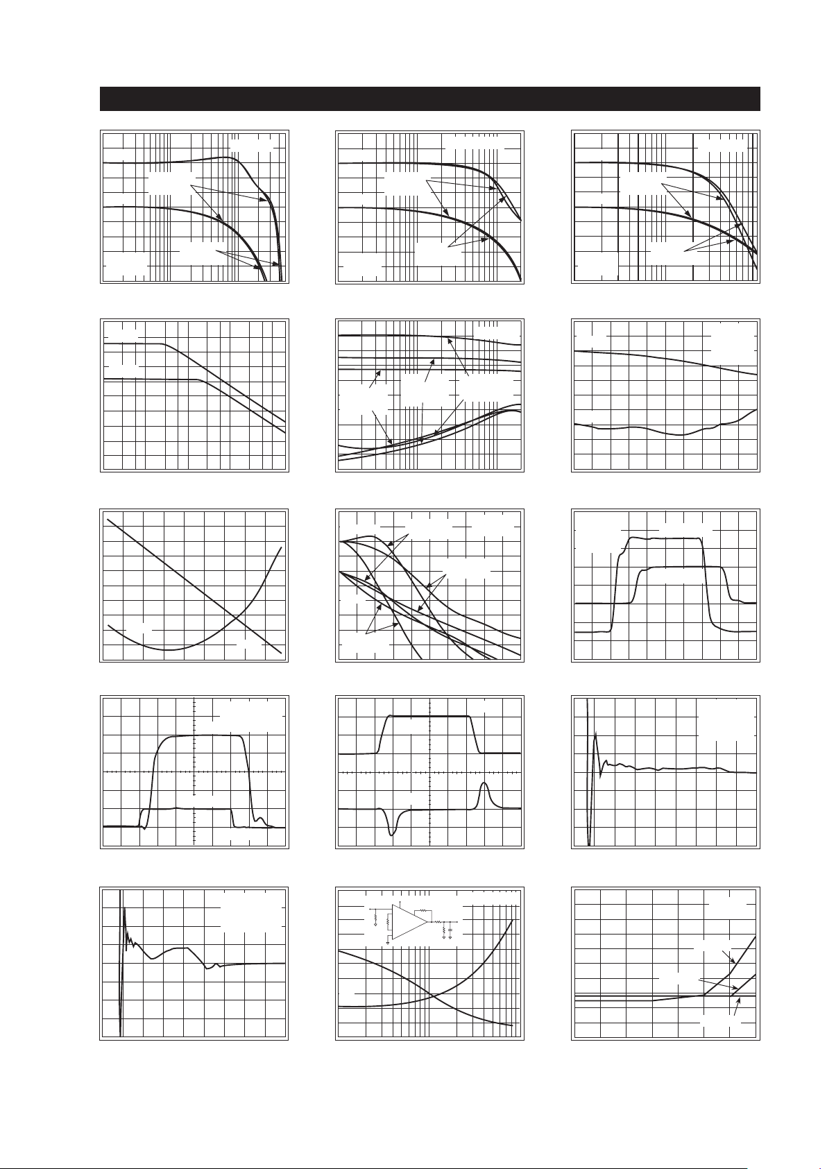
CLC522TypicalPerformance
(TA=+25°C, Vcc=±5V, Av=+10, Vg=1.1V, RL=100Ω; unless noted)
0
-45
-90
-135
-180
-270
V
out
= 500m V
pp
Rg=182Ω
R
f
= 1kΩ
A
V=AVmax
(Vg=1.0V)
A
V
=1
(V
g
=-0.8V)
Gain
Phase
1 Frequency (MHz) 200
Normalized Magnitude (1dB/div)
Phase (45°/div)
Frequency Response (A
V
max
=10)
Vin= 25mV
pp
Rg=10.2Ω
R
f
= 715Ω
A
V=AVmax
(Vg=1.0V)
Gain
Phase
1
Frequency (MHz) 100
Normalized Magnitude (1dB/div)
Phase (45°/div)
Frequency Response (A
V
max
=100)
0
-45
-90
-135
-180
-270
AV=1
(V
g
=-0.98V)
V
out
= 2V
pp
Rg=2kΩ
R
f
= 2.2kΩ
A
V=AVmax
(Vg=1.0V)
Gain
Phase
1 Frequency (MHz)
5
00
Normalized Magnitude (1dB/div)
Phase (45°/div)
Frequency Response (A
V
max
=2)
0
-45
-90
-135
-180
-270
AV=1
(V
g
=0V)
100
90
80
70
60
50
40
30
20
10
0
Frequency (Hz)
PSRR/CMRR (dB)
PSRR and CMRR (Input Referred)
CMRR
PSRR
10
4
10
5
10
6
10
7
10
8
Phase
Gain
A
v
max
+ 10
V
o
= 2V
pp
Rf= 1k
V
g
= 1.1V
Magnitude (0.1dB/div)
Deviation from Linear Phase(0.1°/div)
Gain Flatness & Linear Phase Deviation
0
Frequency (3MHz/div)
30MHz
V
g
(Volts)
0.20
0.18
0.16
0.14
0.12
0.10
0.08
0.06
0.04
0.02
0.00
10
0
Full Scale Non-linearity (%)
Gain (V/V)
SGNL vs. Vg, Gain
0.9 0.7 0.5 0.3 0.1 -0.1 -0.3 -0.5 -0.7 -0.9
Frequency (25MHz/div)
0
-45
-90
-135
-180
-225
Magnitude (1dB/div)
Large Signal Frequency Response
Magnitude
Phase
Gain
SGNL
V
o
= 5V
pp
Vg= 1.1V
A
v
max
= +100
R
f
= 806Ω
A
v
max
= +2
R
f
= 2kΩ
A
v
max
= +10
R
f
= 1kΩ
0 250
Phase (deg)
Rf= 1kΩ
V
out
= 0.5V
pp
V
out
=5V
pp
A
v
max
= +10
V
g
=1.0V
Large signal (Volts)
Small Signal (Volts)
Large & Small Signal Pulse Response
Time (5ns/div)
3
2
1
0
-1
-2
-3
+.75
+.50
+.25
0
-.25
-.50
-.75
V
out
V
g
Vg= 1.0V
V
g
= -1.0V
A
v
max
= + 10
V
in
= 0.25V DC
2.5
Vout (0.5V/div.)
Gain Control Settling Time & Delay
Time (5ns/div)
0
100mV/div
Gain Control Channel Feedthrough
Time (5ns/div)
+1V
0
-1V
V
g
Input
Output
V
in
= 0
A
V
max
= + 10
2V output step
V
g
= 1.0V
.2
.15
0.1
.05
0
-.05
-.1
-.15
-.2
Settling Error (%)
Short Term Settling Time
0
100
Time (10ns/div)
A
V
max
= + 10
2V output step
V
g
= 1.0V
.20
.15
.10
.05
0
-.05
-.10
-.15
-.20
Settling Error (%)
Long Term Settling Time
10
-
9
10
-
8
10
-
7
10
-
6
10
-
5
10
-
4
10
-
3
10
-
2
10
-
1
10
0
Time (sec)
Rs
Ts
A
v
max
= +10
Load Capacitance, C
L
(pF)
Settling Time, TS, (ns), to 0.1%
Rs (ohms)
Settling Time vs. Capacitive Load
10 100 1000
50
40
30
20
10
0
100
90
80
70
60
50
40
30
20
10
0
R
s
C
L
Vg=1.0Volt
50Ω
182Ω
1kΩ
1kΩ
CLC522
Frequency (MHz)
V
g
=+1.1V V
g
=-1.1V
55
40
25
10
-5
-20
-35
-50
-65
-80
-95
Gain (dB)
Feed-through Isolation
1 10 100
A
Vmax
=+2
R
f
=2kΩ
A
Vmax
=+10
R
f
=1kΩ
A
Vmax
=+100
R
f
=750Ω
V
o
=2.5V
pp
50
45
40
35
30
25
20
15
10
5
0
02 4 68101214
Settling Time to 0.1% (ns)
Settling Time vs. Gain
Attenuation From Maximum Gain (dB)
R
f
= 2kΩ
V
o
= 1V
pp
A
v
max
=5
A
v
max
= 10
A
v
max
= 20
3 http://www.national.com
Page 4

Theory of Operation
The CLC522 is a linear wideband variable-gain amplifier
as illustrated in Fig 1. A voltage input signal may be
applied differentially between the two inputs (+Vin, -Vin),
or single-endedly by grounding one of the unused inputs.
The CLC522 input buffers convert the input voltage to a
current (IRg) that is a function of the differential input
voltage (V
input
=+V
in
- -Vin) and the value of the gainsetting resistor (Rg). This current (IRg) is then mirrored to
a gain stage with a current gain of 1.85. The voltagecontrolled two-quadrant multiplier attenuates this current
which is then converted to a voltage via the output
amplifier. This output amplifier is a current-feedback op
amp configured as a transimpedance amplifier. It's transimpedance gain is the feedback resistor (Rf). The input
signal, output, and gain control are all voltages. The
output voltage can easily be calculated as seen in Eq. 1.
Eq. 1
Fig. 1
Phase
Negative Sync
Phase
Positive Sync
Gain
Positive Sync
Gain
Negative Sync
4.43 MHz
A
v
max
= +10
V
g
= 1.0V
Number of 150Ω Loads
Differential Gain (%)
DifferentialPhase (degrees)
Differential Gain and Phase
1234
.25
.20
.15
.10
.05
0
.25
.20
.15
.10
.05
0
50MHz
20MHz
10MHz
5MHz
-4
-2
0246810
Output Power (Pout, dBm)
-35
-40
-45
-50
-55
-60
-65
-70
-75
-80
-85
Distortion Level (dBc)
2nd Harmonic Distortion vs. P
out
1.1V
50Ω
P
o
1kΩ
50Ω
50Ω
50Ω
20Ω
182Ω
R
f
V
g
522
50MHz
20MHz
10MHz
5MHz
-4 -2 0 2 4 6 8 10
Output Power (Pout, dBm)
-35
-40
-45
-50
-55
-60
-65
-70
-75
-80
-85
Distortion Level (dBc)
3rd Harmonic Distortion vs. P
out
1.1V
50Ω
50Ω
1kΩ
50Ω
50Ω
20Ω
182Ω
R
f
V
g
522
P
o
Input
Limited
R
f
= 900Ω
Output
Limited
R
f
= 1.4kΩ
0 100
Frequency (MHz)
20
19
18
17
16
15
14
13
12
11
10
-1dB Compression (dBm)
-1dB Compression at Maximum Gain
P
o
P
i
R
g
R
f
50
Ω
50
Ω
50
Ω
20
Ω
50
Ω
522
CLC522TypicalPerformance
(TA=+25°C, Vcc=±5V, Av=+10, Vg=1.1V, RL=100Ω; unless noted)
Phase, Vg= 0.0V
Phase, V
g
= 1.0V
Gain, V
g
= 0.0V
Gain, V
g
= 1.0V
4.43 MHz
Positive Sync
A
v
max
= +2
Number of 150Ω Loads
Differential Gain (%)
DifferentialPhase (degrees)
Differential Gain and Phase
1234
.10
.08
.06
.04
.02
0
.10
.08
.06
.04
.02
0
0 102030405060708090100
Maximum Gain Setting, A
Vmax
(V/V)
100
10
1
Voltage Noise (nV/√Hz)
Input Referred Voltage Noise vs A
Vmax
VI
V
R
out R
g
f
g
=∗∗
+
∗185
1
2
.
sin.ce I
V
R
A
R
R
V
R
input
g
v
f
g
g
g
=
=∗∗
+
185
1
2
Eq. 2
The gain of the CLC522 is therefore a function of three
external variables; Rg, Rf and Vg as expressed in Eq. 2.
The gain-control voltage (Vg) has a ideal input range of
-1V≤V
g
≤
+1V. At Vg=+1V, the gain of the CLC522 is at
its maximum as expressed in Eq. 3.
A
R
R
V
f
g
max
.=185
Eq. 3
Notice also that Eq. 3 holds for both differential and
single-ended operation.
Choosing Rf and R
g
Rg is calculated from Eq.4.
V
input
max
is the maximum peak
R
V
I
g
input
R
g
=
max
max
Eq. 4
input voltage (Vpk) determined by the application.
I
Rg
max
is the maximum allowable current through Rg and is
typically 1.8mA. Once
A
V
max
is determined from the
minimum input and desired output voltages, Rf is then
determined using Eq. 5. These values of Rf and Rg are
RRA
fgV
=∗∗
1
185.
max
Eq. 5
the minimum possible values that meet the input voltage
and maximum gain constraints. Scaling the resistor
values will decrease bandwidth and improve stability.
Application Discussion
http://www.national.com 4
Page 5

Fig. 2 illustrates the resulting CLC522 bandwidths as a
function of the maximum and minimum input voltages
when V
out
is held constant at 1Vpp.
Adjusting Offsets
Treating the offsets introduced by the input and output
stages of the CLC522 is easily accomplished with a two
step process. The offset voltage of the output stage is
treated by first applying -1.1Volts on Vg, which effectively
isolates the input stage and multiplier core from the
output stage. As illustrated in Fig. 3, the trim pot located
at R14 on the CLC522 Evaluation Board should then be
adjusted in order to null the offset voltage seen at the
CLC522's output (pin 10). Once this is accomplished, the
offset errors introduced by the input stage and multiplier
core can then be treated. The second step requires the
absence of an input signal and matched source impedances on the two input pins in order to cancel the bias
current errors. This done then +1.1Volts should be
applied to Vg and the trim pot located at R10 adjusted in
order to null the offset voltage seen at the CLC522's
output. If a more limited gain range is anticipated, the
above adjustments should be made at these operating
points.
Gain Errors
The CLC522's gain equation as theoretically expressed
in Eq. 2 must include the device's error terms in order to
yield the actual gain equation. Each of the gain error
Fig. 2
Fig. 3
terms are specified in the Electrical Characteristics table
and are defined below and illustrated in Fig. 4.
GACCU : error of
A
V
max
, expressed as ±dB.
GCNL : deviation from theoretical expressed as ±%.
V
g
high
: voltage on Vg producing
A
V
max
.
V
g
low
: voltage on Vg producing
A
V
min
= 0V/V.
∆
V
g
high
,
∆
V
g
low
: error of
V
g
high
,
V
g
low
expresed as ±mV.
Combining these error terms with Eq. 2 gives the "gain
envelope" equation and is expressed in Eq. 7. From the
Electrical Characteristics table, the nominal endpoint
values of Vg are:
V
g
high
=+990mV and
V
g
low
= -975mV.
Signal-Channel Nonlinearity
Signal-channel nonlinearity, SGNL, also known as integral
endpoint linearity, measures the non-linearity of an
amplifier’s voltage transfer function. The CLC522's SGNL,
as it is specified in the Electrical Characteristics table, is
measured while the gain is set at its maximum (i.e.
Vg=+1.1V). The Typical Performance Characteristics
plot labled "SGNL & Gain vs Vg" illustrates the CLC522's
SGNL as Vg is swept through its full range. As can be
seen in this plot, when the gain as reduced from
A
V
max
,
SGNL improves to < 0.02%(-74dB) at Vg=0 and then
degrades somewhat at the lowest gains.
Noise
Fig. 5 describes the CLC522's input-refered spot noise
density as a function of
A
V
max
. The plot includes all the
noise contributing terms. At
A
V
max
= 10V/V, the CLC522
has a typical input-referred spot noise density (eni) of
5.8nV/√Hz. The input RMS voltage noise can be determined from the following single-pole model:
Eq. 8
Further discussion and plots of noise and the noise model
is provided in Application Note OA-23. Comlinear also
provides SPICE models that model internal noise and
other parameters for a typical part.
A
Vmax
A
V
A
Vmin
V
g
low
V
g
high
V
g
±GCNL
±GACCU
±∆V
g
high
±∆V
g
low
Fig. 4
Eq . 7
AA
VV V
VVVV
V GCNL
VV
GACCU
gg g
gggg
g
low low
high high low low
=
−±
()
±−±
()
±−
()
±
max
10
1
20
2
∆
∆∆
V e dBbandwidth
RMS
in
=∗ ∗−
()
157 3.
5 http://www.national.com
Page 6

Component parasitics also influence high frequency
results, therefore it is recommended to use metal film
resistors such as RN55D or leadless components such
as surface mount devices. High profile sockets are not
recommended. If socketing is necessary, it is recommended to use low impedance flush mount connector
jacks such as Cambion (P/N 450-2598).
Application Circuits
Four-Quadrant Multiplier
Applications requiring multiplication, squaring or other
non-linear functions can be implemented with four-quadrant multipliers. The CLC522 implements a four-quadrant multiplier as illustrated in figure 8.
Frequency Shaping
Frequency shaping and bandwidth extension of the
CLC522 can be accomplished using parallel networks
connected across the Rg ports. The network shown in the
Fig. 9 schematic will effectively extend the CLC522's
bandwidth.
2nd Order Tuneable Bandpass Filter
The CLC522 Variable-Gain Amplifier placed into feedback loops provide signal processing functions such as
2nd order tuneable bandpass filters. The center frequency of the 2nd order bandpass illustrated on the front
page is adjusted through the use of the CLC522's gaincontrol voltage, Vg. The integrators implemented with
two CLC420s, provide the coefficients for the transfer
function.
Voltage Noise (nV/√Hz)
Input Referred Voltage Noise vs A
Vmax
0 102030405060708090100
Maximum Gain Setting, A
Vmax
(V/V)
100
10
1
Circuit Layout Considerations
Please refer to the CLC522 Evaluation Board Literature
for precise layout guidelines. Good high-frequency operation requires all of the de-coupling capcitors shown in
Fig. 6 to be placed as close as possible to the power
supply pins in order to insure a proper high-frequency
low-impedance bypass. Adequate ground plane and lowinductive power returns are also required of the layout.
Minimizing the parasitic capacitances at pins 3, 4, 5, 6, 9,
10 and 12 as shown in Fig. 7 will assure best high
frequency performance. Vref (pin 9) to ground should
include a small resistor value of 25 ohms or greater to
buffer the internal voltage follower. The parasitic inductance of component leads or traces to pins 4, 5 and 9
should also be kept to a minimum. Parasitic or load
capacitance, CL, on the output (pin 10) degrades phase
margin and can lead to frequency response peaking or
circuit oscillation. This should be treated with a small
series resistor between output (pin 10) and CL (see the
plot “Settling Time vs. Capacitive Load" for a recommended series resistance).
Fig. 5
Fig. 6
Fig. 7
R
f
R
g
R
T
50Ω
50Ω
50Ω
V
baseband
V
out
V
carrier
25Ω
10
12
3
4
2
9
5
6
CLC522
R
m
=
2R
g
1.85
R1= R
T
|| Rm|| R
s
R
1
R
s
R
T
=
RmR
s
Rm-R
s
Fig. 8
Fig. 9
http://www.national.com 6
Page 7

This page intentionally left blank.
7 http://www.national.com
Page 8

CLC522
Wideband Variable-Gain Amplifier
http://www.national.com
8
Customer Design Applications Support
National Semiconductor is committed to design excellence. For sales, literature and technical support, call the
National Semiconductor Customer Response Group at 1-800-272-9959 or fax 1-800-737-7018.
Life Support Policy
National’s products are not authorized for use as critical components in life support devices or systems without the express written approval
of the president of National Semiconductor Corporation. As used herein:
1. Life support devices or systems are devices or systems which, a) are intended for surgical implant into the body, or b) support or
sustain life, and whose failure to perform, when properly used in accordance with instructions for use provided in the labeling, can
be reasonably expected to result in a significant injury to the user.
2. A critical component is any component of a life support device or system whose failure to perform can be reasonably expected to
cause the failure of the life support device or system, or to affect its safety or effectiveness.
National Semiconductor National Semiconductor National Semiconductor National Semiconductor
Corporation Europe Hong Kong Ltd. Japan Ltd.
1111 West Bardin Road Fax: (+49) 0-180-530 85 86 2501 Miramar Tower Tel: 81-043-299-2309
Arlington, TX 76017 E-mail: europe.support.nsc.com 1-23 Kimberley Road Fax: 81-043-299-2408
Tel: 1(800) 272-9959 Deutsch Tel: (+49) 0-180-530 85 85 Tsimshatsui, Kowloon
Fax: 1(800) 737-7018 English Tel: (+49) 0-180-532 78 32 Hong Kong
Francais Tel: (+49) 0-180-532 93 58 Tel: (852) 2737-1600
Italiano Tel: (+49) 0-180-534 16 80 Fax: (852) 2736-9960
National does not assume any responsibility for use of any circuitry described, no circuit patent licenses are implied and National reserves the right at any time without notice to change said
circuitry and specifications.
 Loading...