

Datasheet CLC502MDC, CLC502AMC, CLC502AJP, CLC502AJE-TR13, CLC502AD-MLS Datasheet (NSC)
...Page 1
Features
■
Output clamping with fast recovery
■
0.0025% settling in 25ns (32ns max.)
■
Low power, 170mW
■
Low distortion. -50dBc at 20MHz
Applications
■
Output clamping applications
■
High-accuracy A/D systems (12-14 bits)
■
High-accuracy D/A converters
■
Pulse amplitude modulation systems
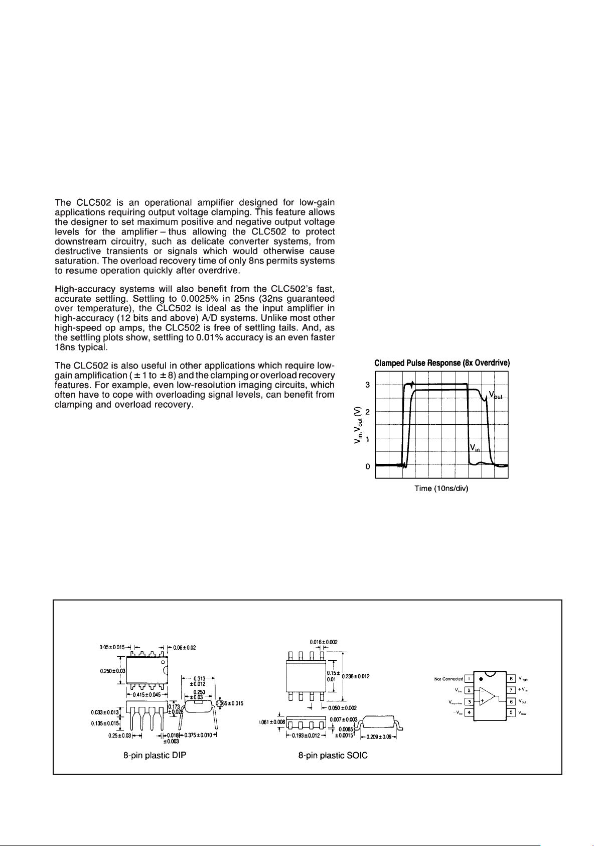
General Description
CLC502
Clamping, Low-Gain Op Amp with Fast 14-bit Settling
N
June 1999
CLC502
Clamping, Low-Gain Op Amp with Fast 14-bit Settling
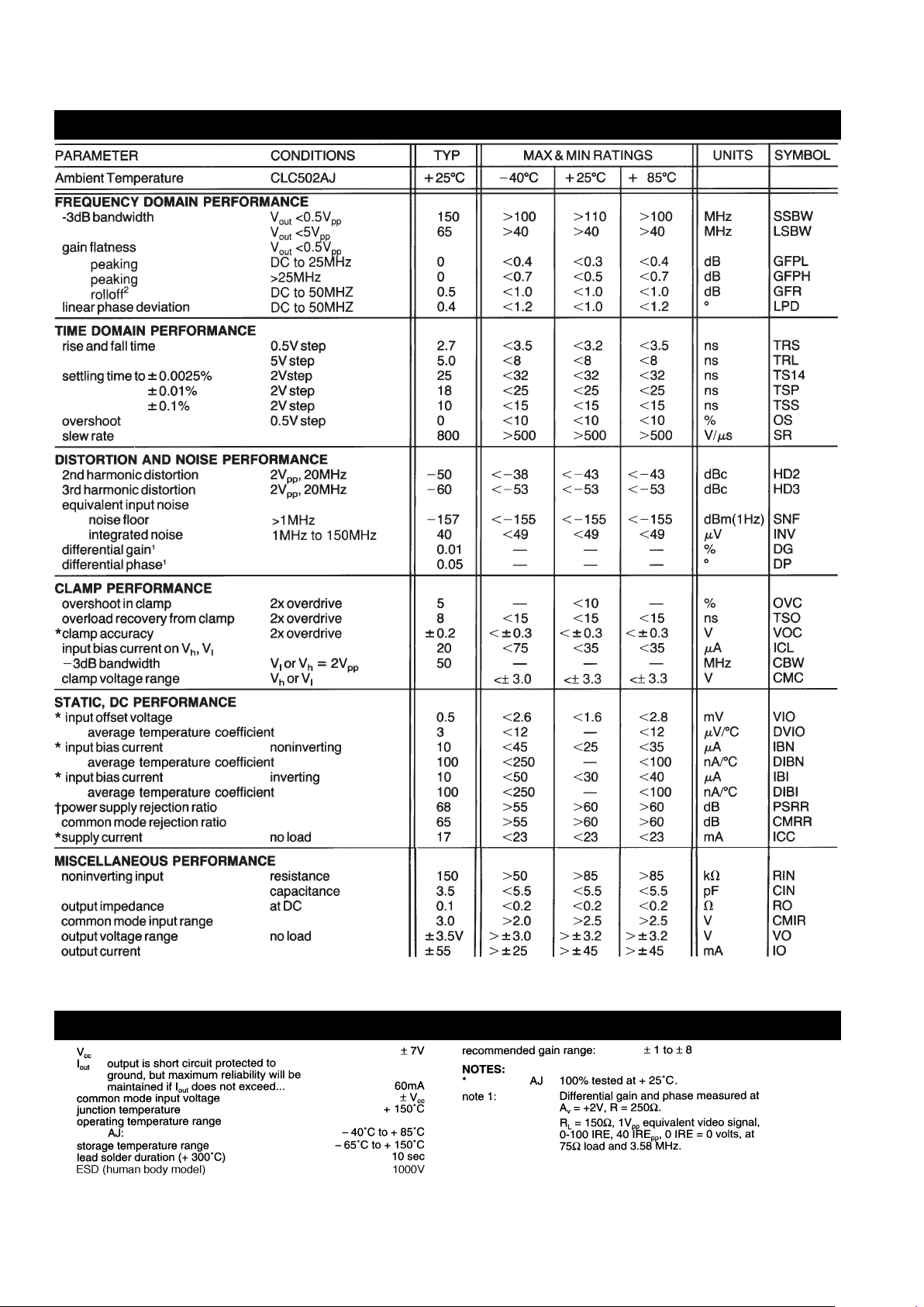
Package Dimensions
Pinout
DIP & SOIC
© 1999 National Semiconductor Corporation http://www.national.com
Printed in the U.S.A.
The CLC502 is available in several versions to meet a variety of
requirements. A three-letter suffix deter mines the version:
CLC502AJP -40°C to +85°C 8-pin plastic DIP
CLC502AJE -40°C to +85°C 8-pin plastic SOIC
DESC SMD number: 5962-91743
Page 2
CLC502 Electrical Characteristics
(Av= +2,Vcc= ±5V,RL= 100Ω,Rf= 250Ω,VH= +3V, VL= -3V)
Absolute Maximum Ratings Miscellaneous Ratings
http://www.national.com 2
Min/max ratings are based on product characterization and simulation. Individual parameters are tested as noted. Outgoing quality levels are
determined from tested parameters.
Page 3

Typical Performance Characteristics
(TA= 25°, Av= +2,VCC= ±5V, RL= 100
ΩΩ,,
Rf= 250ΩΩ,VH= +3V,VL= -3V )
Non-Inverting Frequency Response
Magnitude (1dB/div)
1
10 100
Phase (deg)
-180
-450
-270
-360
-90
0
V
out
= 0.5V
pp
Av = 2
Rf = 249Ω
Av = 1
Rf = 301Ω
Av = 8
Rf = 110Ω
Av = 4
Rf = 200Ω
Frequency (MHz)
Inverting Frequency Response
Magnitude (1dB/div)
1
10 100
Phase (deg)
-360
-630
-450
-540
-270
-180
V
out
= 0.5V
pp
Av = -2
Rf = 237Ω
Av = -1
Rf = 249Ω
Av = -8
Rf = 210Ω
Av = -4
Rf = 249Ω
Frequency (MHz)
3 http://www.national.com
Page 4

http://www.national.com 4
Page 5

5 http://www.national.com
Pac kage Thermal Resistance
Package
θθ
JC
θθ
JA
AJP 65°C/W 120°C/W
AJE 60°C/W 140°C/W
Reliability Information
Transistor Count 46
Page 6

CLC502
Clamping, Low-Gain Op Amp with Fast 14-bit Settling
http://www.national.com 6
Customer Design Applications Support
National Semiconductor is committed to design excellence. For sales, literature and technical support, call the
National Semiconductor Customer Response Group at 1-800-272-9959 or fax 1-800-737-7018.
Life Support Policy
National’s products are not authorized for use as critical components in life support devices or systems without the express written approval of
the president of National Semiconductor Corporation. As used herein:
1. Life support devices or systems are devices or systems which, a) are intended for surgical implant into the body, or b) support or
sustain life, and whose failure to perfor m, when proper ly used in accordance with instructions for use provided in the labeling, can
be reasonably expected to result in a significant injury to the user.
2. A critical component is any component of a life support device or system whose failure to perform can be reasonably expected to
cause the failure of the life support device or system, or to affect its safety or effectiveness.
National Semiconductor National Semiconductor National Semiconductor National Semiconductor
Corporation Europe Hong Kong Ltd. Japan Ltd.
1111 West Bardin Road Fax:(+49) 0-180-530 85 86 2501 Miramar Tower Tel: 81-043-299-2309
Arlington, TX 76017 E-mail: europe.support.nsc.com 1-23 Kimberley Road Fax:81-043-299-2408
Tel: 1(800) 272-9959 Deutsch Tel: (+49) 0-180-530 85 85 Tsimshatsui, Kowloon
Fax:1(800) 737-7018 English Tel: (+49) 0-180-532 78 32 Hong Kong
Francais Tel: (+49) 0-180-532 93 58 Tel: (852) 2737-1600
Italiano Tel: (+49) 0-180-534 16 80 Fax: (852) 2736-9960
National does not assume any responsibility for use of any circuitry described, no circuit patent licenses are implied and National reserves the right at any time without notice to change said
circuitry and specifications.
N
 Loading...