

Page 1
Features
■
400MHz bandwidth (Av = +2)
■
5mA supply current
■
0.02%, 0.03° differential gain, phase
■
2000V/µs slew rate
■
9ns settling to 0.1%
■
0.05dB gain flatness to 100MHz
■
-65/-78dBc HD2/HD3
Applications
■
High resolution video
■
A/D driver
■
Medical imaging
■
Video switchers & routers
■
RF/IF amplifier
■
Communications
■
Instrumentation
General Description
The National CLC446 is a very high-speed unity-gain-stable current-feedback op amp that is designed to deliver the highest levels of performance from a mere 50mW quiescent power. It provides a very wide 400MHz bandwidth, a 2000V/µs slew rate and
900ps rise/fall times. The CLC446 achieves its superior speedvs-power using an advanced complementary bipolar IC process
and National’s current-feedback architecture.
The CLC446 is designed to drive video loads with very low
differential gain and phase errors (0.02%, 0.03°). Combined with
its very low power (50mW), the CLC446 makes an excellent
choice for NTSC/PAL video switchers and routers. With its very
quick edge rates (900ps) and high slew rate (2000V/µs), the
CLC446 also makes an excellent choice for high-speed, highresolution component RGB video systems.
The CLC446 makes an excellent low-power high-resolution A/D
converter driver with its very fast 9ns settling time (to 0.1%) and
low harmonic distortion.
The combination of high performance and low power make
the CLC446 useful in many high-speed general purpose
applications. Its current-feedback architecture maintains consistent
performance over a wide gain range and signal levels. DC gain
and bandwidth can be set independently. Also, either maximally
flat AC response or linear phase response can be emphasized.
V
in
R
4
R
f
+
-
R
g
C
2
CLC446
C
5
V
o
R
5
R
1
R
2
C
3
C
4
R
3
C
1
Typical Application
Elliptic-Function Low Pass Filter
CLC446
400MHz, 50mW Current-Feedback Op Amp
Non-Inverting
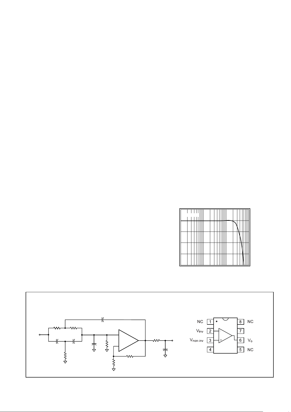
Frequency Response (Av = +2)
Gain (dB)
Frequency (Hz)
8
6
1M
1G
2
-2
4
0
10M 100M
Vo = 0.5V
pp
V
EE
V
CC
Pinout
DIP & SOIC
November 1998
CLC446
400MHz, 50mW Current-Feedback Op Amp
N
© 1998 National Semiconductor Corporation http://www.national.com
Printed in the U.S.A.
Page 2
http://www.national.com 2
Electrical Characteristics
(AV= +2, Rf= 249Ω:VCC= + 5V, RL= 100Ω; unless specified)
PARAMETERS CONDITIONS TYP MIN/MAX RATINGS UNITS NOTES
Ambient Temperature CLC446AJ +25˚C +25˚C 0 to 70˚C -40 to 85˚C
FREQUENCY DOMAIN RESPONSE
-3dB bandwidth V
o
< 0.2V
pp
400 340 300 300 MHz
V
o
< 2.0V
pp
280 210 190 190 MHz
gain flatness V
o
< 2.0V
pp
<100MHz ±0.05 ±0.2 ±0.2 ±0.2 dB
linear phase dev. V
o
< 2.0V
pp
<100MHz 0.2 0.5 0.8 0.8 deg
differential gain NTSC, R
L
=150Ω 0.02 0.04 0.04 0.04 %
differential phase NTSC, R
L
=150Ω 0.03 0.05 0.05 0.05 deg
TIME DOMAIN RESPONSE
rise and fall time 2V step 0.9 1.4 1.5 1.6 ns
settling time to 0.1% 2V step 9 13 15 15 ns
overshoot 2V step 6 15 18 18 %
slew rate 2V step, ±0.5V crossing 2000 1400 1300 1200 V/µs
DISTORTION AND NOISE RESPONSE
2
nd
harmonic distortion 2Vpp, 5MHz -65 -59 -58 -58 dBc
2V
pp
, 20MHz -55 -48 -48 -48 dBc
2V
pp
, 50MHz -54 -43 -42 -42 dBc
3
rd
harmonic distortion 2Vpp, 5MHz -78 -70 -68 -68 dBc
2V
pp
, 20MHz -70 -62 -60 -60 dBc
2V
pp
, 50MHz -50 -45 -42 -42 dBc
equivalent input noise
voltage (e
ni
) >1MHz 3.8 4.8 5.0 5.1 nV/√Hz
non-inverting current (i
bn
) >1MHz 2.0 2.6 2.8 3.3 pA/√Hz
inverting current (i
bi
) >1MHz 16 19 20 21 pA/√Hz
STATIC DC PERFORMANCE
input offset voltage 2 7 10 11 mV A
average drift 17 – 25 35 µV/˚C
input bias current non-inverting 3 12 25 25 µAA
average drift 30 – 90 130 nA/˚C
input bias current inverting 10 22 30 35 µAA
average drift 26 – 75 85 nA/˚C
power supply rejection ratio DC 52 45 43 43 dB
common-mode rejection ratio DC 48 44 42 42 dB
supply current R
L
= ∞ 4.8 5.8 6.2 6.2 mA A
MISCELLANEOUS PERFORMANCE
input resistance non-inverting 1.5 1.0 0.85 0.70 MΩ
input capacitance non-inverting 1 2 2 2 pF
input range common-mode ±2.8 ±2.6 ±2.4 ±2.3 V
output voltage range R
L
= 100Ω ±3.1 ±2.8 ±2.8 ±2.6 V
R
L
= ∞ ±3.2 ±3.0 ±2.9 ±2.8 V
output current 48 48 48 48 mA
output resistance, closed loop DC 0.04 0.1 0.1 0.1 Ω
Min/max ratings are based on product characterization and simulation. Individual parameters are tested as noted. Outgoing quality levels are
determined from tested parameters.
Absolute Maximum Ratings
supply voltage
±
6V
output current ±48mA
common-mode input voltage
±
Vcc
maximum junction temperature +175˚C
storage temperature range -65˚C to +150˚C
lead temperature (soldering 10 sec) +300˚C
ESD rating (human body model) 1000V
Notes
A) J-level: spec is 100% tested at +25˚C.
Ordering Information
Model Temperature Range Description
CLC446AJP -40˚C to +85˚C 8-pin PDIP
CLC446AJE -40˚C to +85˚C 8-pin SOIC
CLC446ALC -40˚C to +85˚C dice
CLC446A8B -55˚C to +125˚C 8-pin CerDIP, MIL-STD-883
CLC446AMC -55˚C to +125˚C dice, MIL-STD-883
Contact the factory for other packages and DESC SMD number.
Package Thermal Resistance
Package
θθ
JC
θθ
JA
Plastic (AJP) 70˚C/W 125˚C/W
Surface Mount (AJE) 60˚C/W 140˚C/W
Ceramic (A8B) 40˚C/W 130˚C/W
Reliability Information
Transistor Count 36
MTBF (based on limited test data) 39Mhr
Page 3
3 http://www.national.com
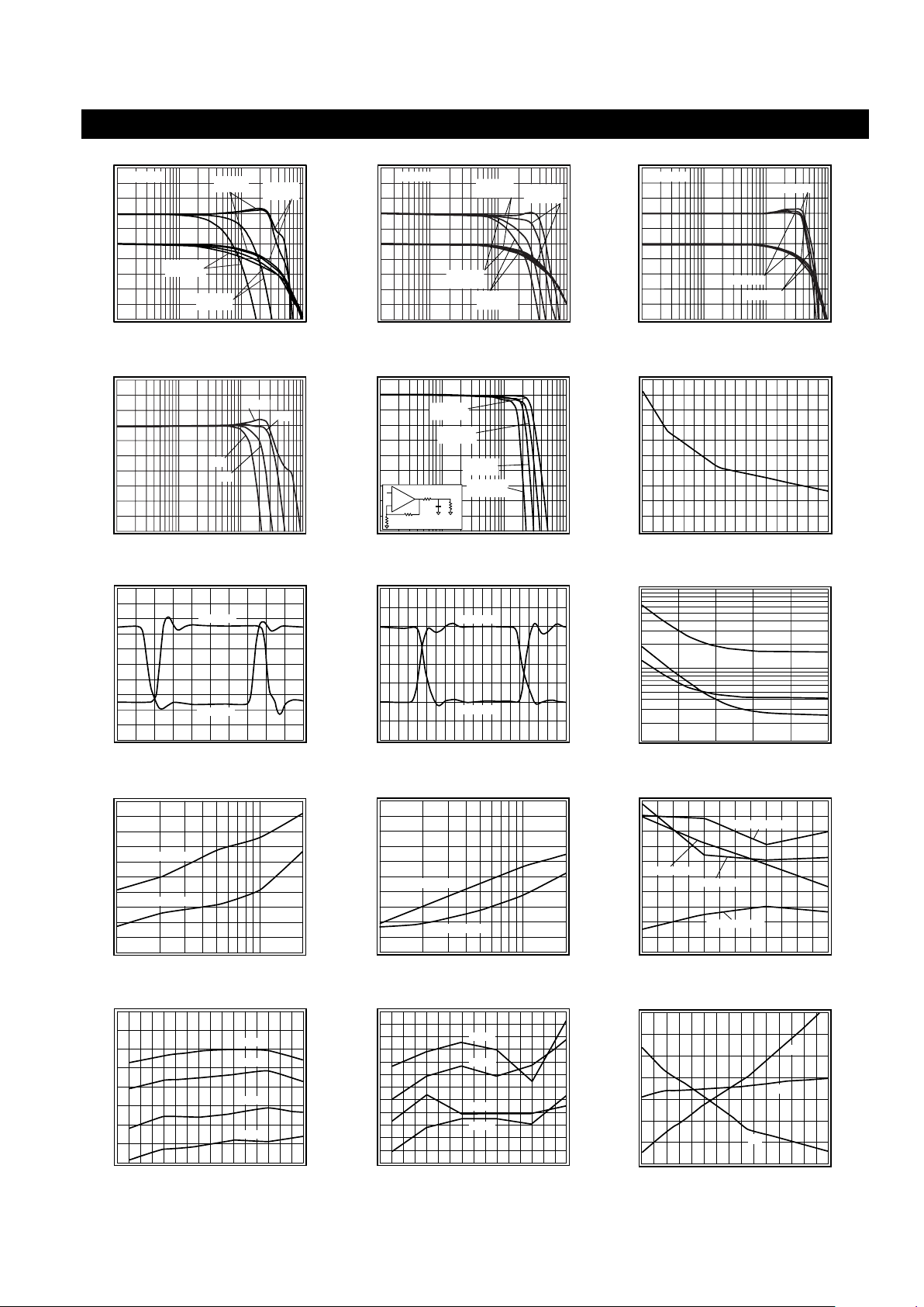
Typical Performance Characteristics
(VCC= ±5V ,Av= +2,Rf=249
ΩΩ,,
RL= 100ΩΩ; unless specified)
Non-Inverting Frequency Response
Normalized Magnitude (1dB/div)
Frequency (Hz)
10M
100M
1G
Vo = 0.5V
pp
Phase (deg)
0
-90
-360
-180
-270
-450
1M
Av = 1V/V
R
f
= 453Ω
Av = 2V/V
Rf = 249Ω
Av = 5V/V
Rf = 200Ω
Av = 10V/V
Rf = 200Ω
Inverting Frequency Response
Normalized Magnitude (1dB/div)
Frequency (Hz)
1M 10M
1G
Phase (deg)
-180
-225
-360
-270
-315
100M
Vo = 0.5V
pp
Av = -1V/V
R
f
= 249Ω
Av = -2V/V
R
f
= 249Ω
Av = -5V/V
R
f
= 200Ω
Av = -10V/V
R
f
= 200Ω
Frequency Response vs. R
L
Normalized Magnitude (1dB/div)
Frequency (Hz)
10M 100M
1G
Phase (deg)
0
-90
-360
-180
-270
-450
1M
RL = 1kΩ
RL = 100Ω
RL = 500Ω
Vo = 0.5V
pp
Frequency Response vs. V
o
Normalized Magnitude (1dB/div)
Frequency (Hz)
1M
10M 100M
1G
0.1V
pp
1V
pp
4V
pp
2V
pp
Frequency Response vs. C
L
Normalized Magnitude (1dB/div)
Frequency (Hz)
1M
10M 100M
1G
CL = 22pF
R
s
= 33.2Ω
CL = 10pF
R
s
= 46.4Ω
CL = 47pF
R
s
= 21Ω
CL = 100pF
R
s
= 13.3Ω
C
L
1k
R
s
+
-
249Ω
249Ω
Recommended Rs vs. C
L
R
s
(Ω)
CL(pF)
40
30
0
10
20
100
20
10
30
40 50 60 70 80 90
50
Small Signal Pulse Response
Output Voltage (0.5V/div)
Time (2ns/div)
Av = +2V/V
Av = -2V/V
Large Signal Pulse Response
Output Voltage (1V/div)
Time (2ns/div)
Av = -2V/V
Av = +2V/V
Equivalent Input Noise
Voltage Noise (nV/
√
Hz)
Frequency (Hz)
100
1
1k
10k 100k
10
Current Noise (pA/
√Hz)
100
1
10
1M 10M
i
bi
e
ni
i
bn
100M
2nd Harmonic Distortion
Distortion (dBc)
Frequency (Hz)
-50
-60
-90
1M
10M
-70
-80
Vo = 2V
pp
-100
2nd RL = 100Ω
2nd RL = 1kΩ
3rd Harmonic Distortion
Distortion (dBc)
Frequency (Hz)
-60
-70
-100
1M
10M
-80
-90
Vo = 2V
pp
-50
3rd RL = 100Ω
3rd RL = 1kΩ
Differential Gain and Phase (3.58MHz)
Differential Gain (%)
Number of 150Ω Loads
0.01
0
-0.03
1
2
3
-0.01
-0.02
Differential Phase (deg)
-0.04
-0.08
-0.2
-0.12
-0.16
-0.04
0
4
Phase Pos Sync
Phase Neg Sync
Gain Pos Sync
Gain Neg Sync
2nd Harmonic Distortion vs. P
out
Distortion (dBc)
Output Power (dBm)
-40
-50
-80
-4
-2 0
-60
-70
2
4
68
10 12
10MHz
5MHz
2MHz
1MHz
3rd Harmonic Distortion vs. P
out
Distortion (dBc)
Output Power (dBm)
-65
-70
-85
-4
-2
-75
-80
-90
-95
02
46
81012
10MHz
5MHz
2MHz
1MHz
Vos, IBN, & IBI vs. Temperature
V
os
(mV)
Temperature (°C)
2
1
-60
-40
-20
0
-1
I
BI
, I
BN
(µA)
2
-2
-6
-10
0
20 40
60 80
I
BN
V
os
I
BI
Page 4
http://www.national.com 4
The CLC446 has a current-feedback architecture built in
an advanced complementary bipolar process. The key
features of current-feedback are:
■
AC bandwidth is independent of voltage gain
■
Unity-gain stability
■
Frequency response may be adjusted with R
f
■
High slew rate
■
Low variation in performance for a wide range
of gains, signal levels and loads
■
Fast settling
Current-feedback operation can be explained with a
simple model. The voltage gain for the circuits in Figures
1 and 2 is approximately:
where
■
Avis the DC voltage gain
■
Rfis the feedback resistor
■
Z(jω) is the CLC446’s open-loop
transimpedance gain
■
is the loop-gain
The denominator of the equation above is approximately
1 at low frequencies. Near the -3dB corner
frequency, the interaction between Rfand Z(jω)
dominates the circuit performance. Increasing Rfdoes
the following:
■
Decreases loop-gain
■
Decreases bandwidth
■
Lowers pulse response overshoot
■
Reduces gain peaking
■
Affects frequency response phase linearity
CLC446 Operation
The following topics will supply you with:
■
Design parameters, formulas and techniques
■
Interfaces
■
Application circuits
■
Layout techniques
■
SPICE model information
DC Gain (non-inverting)
The non-inverting DC voltage gain for the configuration
shown in Figure 1 is .
The normalized gain plots in the
Typical Performance
Characteristics
section show different feedback
resistors (Rf) for different gains. These values of Rfare
recommended for obtaining the highest bandwidth with
minimal peaking. The resistor Rtprovides DC bias for
the non-inverting input.
For Av< 5, use linear interpolation on the nearest Avvalues to calculate the recommended value of Rf. For Av≥
5, the minimum recommended Rfis 200Ω.
Select Rgto set the DC gain: .
DC gain accuracy is usually limited by the tolerance of R
f
and Rg.
Figure 1: Non-Inverting Gain
+
-
CLC446
R
f
0.1µF
6.8µF
V
o
V
in
V
CC
0.1µF
6.8µF
V
EE
3
2
4
7
6
+
+
R
g
R
t
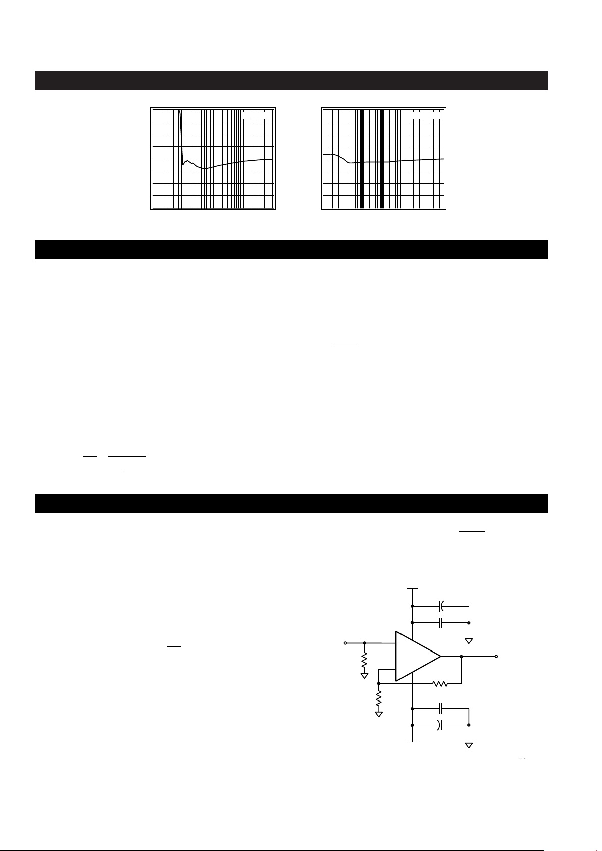
Typical Performance Characteristics
(VCC= ±5V, Av= +2, Rf= 249
ΩΩ,,
RL= 100ΩΩ; unless specified)
Short Term Settling Time
V
o
(% Output Step)
Time (sec)
0.2
0.1
-0.2
1n
10n
100n
0
-0.1
1
µ
10
µ
VO = 2V step
Long Term Settling Time
V
o
(% Output Step)
Time (s)
0.2
0.1
-0.2
1
µ
10
µ
100
µ
0
-0.1
1m
10m
100m 1
VO = 2V step
V
V
A
1
R
Zj
o
in
v
f
=
+
()
ω
Zj
R
f
ω
()
A1
R
R
v
f
g
=+
R
R
A1
g
f
v
=
−
CLC446 Design Information
Page 5

5 http://www.national.com
DC Gain (unity gain buffer)
The recommended Rffor unity gain buffers is 453Ω. R
g
is left open. Parasitic capacitance at the inverting node
may require a slight increase of Rfto maintain a flat
frequency response.
DC Gain (inverting)
The inverting DC voltage gain for the configuration
shown in Figure 2 is .
Figure 2: Inverting Gain
The normalized gain plots in the
Typical Performance
Characteristics
section show different feedback
resistors (Rf) for different gains. These values of Rfare
recommended for obtaining the highest bandwidth with
minimal peaking. The resistor Rtprovides DC bias for the
non-inverting input.
For |Av| < 5, use linear interpolation on the nearest Avvalues to calculate the recommended value of Rf. For |Av|
≥ 5, the minimum recommended Rfis 200Ω.
Select Rgto set the DC gain: . At large
gains, Rg becomes small and will load the previous stage.
This can be solved by driving Rgwith a low impedance
buffer like the CLC111, or increasing Rfand Rg.
See the
AC Design (small signal bandwidth)
sub-section for the tradeoffs.
DC gain accuracy is usually limited by the tolerance of R
f
and Rg.
DC Gain (transimpedance)
Figure 3 shows a transimpedance circuit where the current Iinis injected at the inverting node. The current
source’s output resistance is much greater than Rf.
The DC transimpedance gain is:
The recommended Rfis 453Ω. Parasitic capacitance at
the inverting node may require a slight increase of Rfto
maintain a flat frequency response.
DC gain accuracy is usually limited by the tolerance of Rf.
Figure 3: Transimpedance Gain
DC Design (level shifting)
Figure 4 shows a DC level shifting circuit for inverting
gain configurations. V
ref
produces a DC output level
shift of , which is independent of the DC
output produced by Vin.
Figure 4: Level Shifting Circuit
DC Design (single supply)
Figure 5 is a typical single-supply circuit. R1and R2form
a voltage divider that sets the non-inverting input DC voltage. This circuit has a DC gain of 1. A low
frequency zero is set by Rgand C2. The coupling capacitor C1isolates its DC bias point from the
previous stage. Both capacitors make a high pass
response; high frequency gain is determined by Rfand Rg.
Figure 5: Single Supply Circuit
The complete gain equation for the circuit in Figure 5 is:
A
R
R
v
f
g
=−
+
-
CLC446
R
f
0.1µF
6.8µF
V
o
V
in
V
CC
0.1µF
6.8µF
V
EE
R
g
R
t
3
2
4
7
6
+
+
R
R
A
g
f
v
=
A
V
I
R
R
o
in
f
==−
+
-
CLC446
R
f
0.1µF
6.8µF
V
o
V
CC
0.1µF
6.8µF
V
EE
R
t
3
2
4
7
6
+
+
I
in
V
in
R
g
+
-
CLC446
R
f
V
o
V
ref
R
ref
R
t
+
-
CLC446
R
f
V
o
V
in
V
CC
R
g
R
2
R
1
V
CC
C
1
C
2
V
Vs1s
1s 1
R
R
1s
o
in
1
1
2
f
g
2
=
+
⋅
+⋅+
+
τ
τ
τ
τ
−⋅V
R
R
ref
f
ref
Page 6

http://www.national.com 6
where
DC Design (DC offsets)
The DC offset model shown in Figure 6 is used to
calculate the output offset voltage. The equation for output offset voltage is:
The current offset terms, IBNand IBI,
do not track each
other
. The specifications are stated in terms of magnitude only . Therefore, the terms Vos, IBN, and IBIcan have
either polarity. Matching the equivalent resistance seen
at both input pins does not reduce the output
offset voltage.
Figure 6: DC Offset Model
DC Design (output loading)
RL, Rf, and Rgload the op amp output. The equivalent
load seen by the output in Figure 6 is:
R
L(eq)
= RL|| (Rf+ R
eq2
), non-inverting gain
R
L(eq)
= RL|| Rf, inverting gain
R
L(eq)
needs to be large enough so that the minimum output current can produce the required output voltage
swing.
AC Design (small signal bandwidth)
The CLC446 current-feedback amplifier bandwidth is
a function of the feedback resistor (Rf), not of the DC
voltage gain (AV). The bandwidth is approximately
proportional to . As a rule, if Rfdoubles, the bandwidth is cut in half. Other AC specifications will also be
degraded. Decreasing Rffrom the recommended value
increases peaking, and
for very small values of
R
f
oscil-
lation will occur
.
AC Design (minimum slew rate)
Slew rate influences the bandwidth of large signal
sinusoids. To determine an approximate value of slew
rate necessary to support a large sinusoid, use the
following equation:
SR ≅ 5 •f •V
peak
where V
peak
is the peak output sinusoidal voltage.
The slew rate of the CLC446 in inverting gains is always
higher than in non-inverting gains.
AC Design (linear phase/constant group delay)
The recommended value of Rfproduces minimal
peaking and a reasonably linear phase response.
To improve phase linearity when |Av| < 5, increase R
f
approximately 50% over its recommended value. Some
adjustment of Rfmay be needed to achieve phase linearity for your application. See the
AC Design (small
signal bandwidth)
sub-section for other effects of
changing Rf.
Propagation delay is approximately equal to group delay.
Group delay is related to phase by this equation:
where φ(f) is the phase in degrees. Linear phase implies
constant group delay. The technique for achieving linear
phase also produces a constant group delay.
AC Design (peaking)
Peaking is sometimes observed with the recommended
Rf. If a small increase in Rfdoes not solve the problem,
then investigate the possible causes and remedies
listed below.
■
Capacitance across R
f
■
Do not place a capacitor across R
f
■
Use a resistor with low parasitic
capacitance for R
f
■
A capacitive load
■
Use a series resistor between the output and
a capacitive load (see the
Recommended
Rsvs. C
L
plot)
■
Long traces and/or lead lengths between Rfand
the CLC446
■
Keep these traces as short as possible
For non-inverting and transimpedance gain configurations:
■
Extra capacitance between the inverting pin
and ground (Cg)
■
See the
Printed Circuit Board Layout
sub-
section below for suggestions on reducing C
g
■
Increase Rfif peaking is still observed after
reducing C
g
For inverting gain configurations:
■
Inadequate ground plane at the non-inverting pin
and/or long traces between non-inverting pin
and ground
■
Place a 50 to 200Ω resistor between the noninverting pin and ground (see Rtin Figure 2)
Capacitive Loads
Capacitive loads, such as found in A/D converters,
require a series resistor (Rs) in the output to
improve settling performance. The
Recommended
Rsvs. C
L
plot in the
Typical Performance
Characteristics
section provides the information for
selecting this resistor.
sj
RR C
RC
1121
2
g
2
=
=
()
⋅
=⋅
ω
τ
τ
VVIR1
R
R
IR
oos
BN
eq1
f
eq2
BI
f
=− + ⋅
()
⋅+
+⋅
()
R
eq1
R
f
+
-
R
eq2
CLC446
I
BI
I
BN
V
os
V
o
R
L
+
-
1
R
f
τ
φφ
gd
f
1
360
df
df
f
f
=()=−
°
⋅
()
≈−
()
∆
∆
Page 7

7 http://www.national.com
Using a resistor in series with a reactive load will also
reduce the load’s effect on amplifier loop dynamics. For
instance, driving coaxial cables without an output series
resistor may cause peaking or oscillation.
Transmission Line Matching
One method for matching the characteristic impedance
of a transmission line is to place the appropriate resistor
at the input or output of the amplifier. Figure 7 shows the
typical circuit configurations for matching transmission
lines.
Figure 7: Transmission Line Matching
In non-inverting gain applications, Rgis connected
directly to ground. The resistors R1, R2, R6, and R
7
are equal to the characteristic impedance, Zo, of the
transmission line or cable. Use R3to isolate the
amplifier from reactive loading caused by the transmission line, or by parasitics.
In inverting gain applications, R3is connected directly to
ground. The resistors R4, R6, and R7are equal to Zo. The
parallel combination of R5and Rgis also equal to Zo.
The input and output matching resistors attenuate the
signal by a factor of 2, therefore additional gain is needed.
Use C6to match the output transmission line over a greater
frequency range. It compensates for the increase of the op
amp’s output impedance with frequency.
Thermal Design
To calculate the power dissipation for the CLC446,
follow these steps:
1. Calculate the no-load op amp power:
P
amp
= I
CC
•
(VCC– VEE)
2. Calculate the output stage’s RMS power:
Po= (VCC– V
load
) •I
load
, where V
load
and
I
load
are the RMS voltage and current across
the external load.
3. Calculate the total op amp RMS power:
Pt= P
amp
+ P
o
To calculate the maximum allowable ambient temperature, solve the following equation: T
amb
= 175 – P
t
•
θJA,
where θJAis the thermal resistance from junction to
ambient in °C/W, and T
amb
is in °C. The
Package
Thermal Resistance
section contains the thermal
resistance for various packages.
Dynamic Range (input /output protection)
ESD diodes are present on all connected pins for
protection from static voltage damage. For a signal that
may exceed the supply voltages, we recommend using
diode clamps at the amplifier’s input to limit the signals to
less than the supply voltages.
Dynamic Range (input /output levels)
The
Electrical Characteristics
section specifies the
Common-Mode Input Range and Output Voltage Range;
these voltage ranges scale with the supplies.
Output Current is also specified in the
Electrical
Characteristics
section.
Unity gain applications are limited by the Common-Mode
Input Range. At greater non-inverting gains, the Output
Voltage Range becomes the limiting factor. Inverting
gain applications are limited by the Output Voltage
Range. For transimpedance gain applications, the sum
of the input currents injected at the inverting
input pin of the op amp needs to be: ,
where V
max
is the Output Voltage Range (see the
DC
Gain (transimpedance)
sub-section for details).
The equivalent output load needs to be large enough so
that the minimum output current can produce the
required output voltage swing. See the
DC Design (out-
put loading)
sub-section for details.
Dynamic Range (noise)
In RF applications, noise is frequently specified as Noise
Figure (NF). This allows the calculation of signal to noise
ratio into a defined load. Figure 8 plots the NF for a
CLC446 at a gain of 10, and with a feedback resistor R
f
of 100Ω. The minimum NF (3.9dB) occurs when the
source impedance equals 1600Ω.
Figure 8: Noise Figure vs. Source Resistance
Figure 9: Noise Model
+
-
CLC446
R
3
Z
0
R
6
V
o
Z
0
R
1
R
2
+
R
g
Z
0
R
4
R
5
V
1
V
2
+
-
R
f
C
6
R
7
I
V
R
in
max
f
≤
Noise Figure (dB)
Source Resistance (Ω)
20
15
0
10
100
10k
10
5
1k 100k
+
-
CLC446
e
ni
2
V
o
R
s
i
bn
2
+
-
V
s
R
f
i
bi
2
R
g
Page 8

http://www.national.com 8
The CLC446 noise model in Figure 9 is used to develop
this equation for NF:
where:
■
RSis the source resistance at the noninverting input
■
There is no matching resistor from the input
to ground
■
eni, ibn, and ibiare the voltage and current
noise density terms (see the
Electrical
Characteristics
section)
■
■
Rfis the feedback resistor, and Rgis the
gain-setting resistor
To achieve a low Noise Figure while matching the source,
use a matching transformer or the
Low Noise
Composite Amp With Input Matching
circuit found in
the
CLC446 Applications
section.
Dynamic Range (distortion)
The distortion plots in the Typical Performance
Characteristics section show distortion as a function of
load resistance, frequency, and output amplitude.
Distortion places an upper limit on the CLC446’s
dynamic range.
Realized output distortion is highly dependent upon the
external circuit. Some of the common external circuit
choices that can improve distortion are:
■
Short and equal return paths from the load to
the supplies
■
De-coupling capacitors of the correct value
■
Higher load resistance
■
A lower ratio of the output voltage swing to
power supply voltage
Printed Circuit Board Layout
High Frequency op amp performance is strongly dependent on proper layout, proper resistive termination and
adequate power supply decoupling. The most important
layout points to follow are:
■
Use a ground plane
■
Bypass power supply pins with:
■
ceramic capacitors of about 0.1µF placed
less than 0.1" (3mm) from the pin
■
tantalum capacitors of about 6.8µF for large
signal current swings or improved power
supply noise rejection; we recommend a
minimum of 2.2µF for any circuit
■
Minimize trace and lead lengths for components
between the inverting and output pins
■
Remove ground plane underneath the amplifier
package and 0.1" (3mm) from all input/output
pads
■
For prototyping, use flush-mount printed circuit
board pins; never use high profile DIP sockets
Evaluation Board
Separate evaluation boards are available for prototyping
and measurements. Additional information is available in
the evaluation board literature.
Low Noise Composite Amp With Input Matching
The composite amp shown in Figure 10 eliminates the
need for a matching resistor to ground at the input. By
connecting two amplifiers in series, the first noninverting and the second inverting, an overall inverting
gain is realized. The feedback resistor (Rf) closes the
loop, and generates a set input resistance (Rin) that can
be matched to RS. Rfgenerates less noise than a
matching resistor to ground at the input.
Figure 10: Composite Amplifier
The input resistance and DC voltage gain of the
amplifier are:
Match the source resistance by setting: R
in
= RS.
The voltage noise produced by Rf, referred to the source
VS, is:
The noise of a simple input matching resistor connected to
ground can be calculated by setting G to 0 in this equation.
Thus, this circuit reduces the thermal noise power
produced by the matching resistor by a factor of (1+G).
Rectifier Circuit
Wide bandwidth rectifier circuits have many applications.
Figure 11 shows a 200MHz wideband full-wave rectifier
circuit using a CLC446 and a CLC522 amplifier. Schottky
or PIN diodes are used for D1and D2. They produce an
active half-wave rectifier whose signals are taken at the
feedback diode connection. The CLC522 takes the
difference of the two half-wave rectified signals,
producing a full-wave rectifier. The CLC522 is used at a
gain of 5 to achieve high differential bandwidth. For best
NF 10log
e i R 4 TR i R R 4 T R R
4TR
ni2bn
s
2
s
bi
f
g
2
f
g
s
=
+
()
++⋅
()
+⋅
kk
k
4 T 16.0 x 10 J
T
290 K
, Tisin K
21
k =
()
⋅
°
°
−
CLC446 Applications
+
-
CLC446
R
f
V
o
R
g2
-
+
20Ω
CLC446
R
f2
R
f1
R
g1
R
in
V
s
R
s
+
-
R
R
1G
, where G 1
R
R
R
R
V
V
G
R
RR
in
ff1
g1
f2
g2
o
s
in
in
s
=
+
=+
⋅
=− ⋅
+
e4TR
R
R1G
Rf
s
s
in
2
=⋅
⋅+
()
k
Page 9

9 http://www.national.com
high frequency performance, maintain low parasitic
capacitance from the diodes D1and D2to ground, and
from the input of the CLC522 to ground.
Figure 11: Full-Wave Rectifier
Elliptic Low-pass, Anti-aliasing Filter
Elliptic filters are often used in anti-aliasing applications.
If there is noise or undesired signals at frequencies
above 1/2 the sampling rate of an A/D converter, then
these signals are aliased down into the operating
frequency range, degrading the signal of interest. To
filter out these undesired signal components, place a low
pass filter in front of the A/D converter.
The
Typical Application
depicted on the front page is a
10MHz, third-order elliptic filter. It has a voltagecontrolled, voltage source (VCVS) topology using a
CLC446. To calculate the component values for this
filter, do the following:
1. Select the filter approximation function for your
application (see References [1-2]). For this design
we chose:
Filter type = Elliptic
Filter order (n) = 3
Passband ripple = 0.18dB
Mininimum stopband attenuation (A
min
) =
37.44dB
Cuttoff frequency = 10MHz (at 0.18dB
attenuation)
These choices produce the following results:
-3dB frequency = 12.7MHz
Stopband corner frequency = 29.3MHz
2. Find the pole and zero locations. Reference [1]
gave the following for our filter:
Pole 1: α = 0.38621
Pole 2: αo= 0.88668
Zero 1: β = 1.13897
Zero 2: ω∞= 3.3505
3. Denormalize the frequency by multiplying by
the cutoff frequency (ωo) in radians/second.
For our filter we have:
Cutoff frequency: ωo= 2π(10MHz) =
62.832 x 10⁶rad/s
Pole 1: α'= ωoα = 24.266 x 10⁶rad/s
Pole 2: α
o
'
= ωoαo= 55.712 x 10⁶rad/s
Zero 1: β'= ωoβ = 21.052 x 10⁶rad/s
Zero 2: ω
∞
'
= ωoω∞ = 71.564 x 10⁶rad/s
4. Calculate these intermediate coefficients used
in Reference [2].
For this design, a = 0.64226, b = 7.7612 and
c = 75.556 x 10⁶.
5. Set the following resistance and capacitance
scaling factors:
R = an arbitrary value
C = an arbitrary value
We chose C = 47pF and R = 1.00kΩ.
6. Calculate the capacitor, resistor and gain (K)
values using these equations:
For this design, the calculated values are:
C1 = 47pF, C2 = 91pF, C3 = C4 = 23.5pF,
C5 = 17.95pF, R1 = R2 = 202.1Ω, R3 = 101.1Ω,
R4 = 3190Ω, R5 = 1000Ω and K = 4.928.
7. Select the feedback resistor (Rf) and gainsetting resistor (Rg) values to obtain a noninverting voltage gain of Av = K. See the
DC
Gain (non-inverting)
sub-section for details
on selecting these values.
+
-
CLC446
V
o
+
-
500Ω
CLC522
250Ω
250Ω
3
250Ω
D
1
D
2
R
g
162Ω
R
1
50Ω
R
2
50Ω
3
4
5
6
2
R
f
800Ω
R
o
50Ω
20Ω
12
9
10
V
g
R
in
50Ω
V
in
2
6
c''a
2'
c
b
'
c
2
2
2
=
()
+
()
==
∞
αβ
αω
CC
CC
C
2
C
Cb 1
4
R
1
cC b
RR
R
2
R
4b
cC 1 b 4cC
RR
C
1
R'
K2
2C
C
a
2b2Cb
1
cR
aC
1
34
2
3
12
3
4
2
5
5
o
2
4
2
=
==
≥
−
()
=
==
=
−
()
+
=
=
=+ − + ⋅ −
α
Page 10

http://www.national.com 10
Figure 12 shows the ideal response of this filter. Some
methods to bring actual performance closer to this
ideal are:
■
Compensate for op amp delay effects
(pre-distortion)
■
Adjust for parasitic capacitances in the layout
■
Use components with small tolerances
■
Add trim capacitors
Figure 12: Ideal Elliptic Filter Frequency Response
References:
[1] Anatol I. Zverev,
Handbook of FILTER
SYNTHESIS
, John Wiley & Sons, 1967,
p. 177
[2] Arthur B. Williams and Fred J. Taylor,
Electronic Filter Design Handbook
,
McGraw Hill, 1995, pp. 3-29 to 3-31.
Gain (dB)
Frequency (Hz)
20
10
0
-40
1M 10M 100M 1G
-10
-30
-20
Page 11

11 http://www.national.com
This page intentionally left blank.
Page 12

CLC446
400MHz, 50mW Current-Feedback Op Amp
http://www.national.com 12
Customer Design Applications Support
National Semiconductor is committed to design excellence. For sales, literature and technical support, call the
National Semiconductor Customer Response Group at 1-800-272-9959 or fax 1-800-737-7018.
Life Support Policy
National’s products are not authorized for use as critical components in life support devices or systems without the express written approval
of the president of National Semiconductor Corporation. As used herein:
1. Life support devices or systems are devices or systems which, a) are intended for surgical implant into the body, or b) support or
sustain life, and whose failure to perform, when properly used in accordance with instructions for use provided in the labeling, can
be reasonably expected to result in a significant injury to the user.
2. Acritical component is any component of a life support device or system whose failure to perform can be reasonably expected to
cause the failure of the life support device or system, or to affect its safety or effectiveness.
National Semiconductor National Semiconductor National Semiconductor National Semiconductor
Corporation Europe Hong Kong Ltd. Japan Ltd.
1111 West Bardin Road Fax: (+49) 0-180-530 85 86 13th Floor, Straight Block Tel: 81-043-299-2309
Arlington, TX 76017 E-mail: europe.support.nsc.com Ocean Centre, 5 Canton Road Fax: 81-043-299-2408
Tel: 1(800) 272-9959 Deutsch Tel: (+49) 0-180-530 85 85 Tsimshatsui, Kowloon
Fax: 1(800) 737-7018 English Tel: (+49) 0-180-532 78 32 Hong Kong
Francais Tel: (+49) 0-180-532 93 58 Tel: (852) 2737-1600
Italiano Tel: (+49) 0-180-534 16 80 Fax: (852) 2736-9960
National does not assume any responsibility for use of any circuitry described, no circuit patent licenses are implied and National reserves the right at any time without notice to change said
circuitry and specifications.
N
 Loading...