

Page 1
Frequency Response (AV = +2V/V)
Features
■
Unity-gain stable
■
High unity-gain bandwidth: 750MHz
■
Ultra-low differential gain:0.015%
■
Very low differential phase: 0.025°
■
Low power: 70mW
■
Extremely fast slew rate:1500V/µs
■
High output current: 90mA
■
Low noise: 3.5nV/√Hz
■
Dual ±2.5V to ±6V or single 5V to 12V supplies
Applications
■
Professional video
■
Graphics workstations
■
Test equipment
■
Video switching & routing
■
Communications
■
Medical imaging
■
A/D drivers
■
Photo diode transimpedance amplifiers
■
Improved replacement f or CLC420 or OPA620
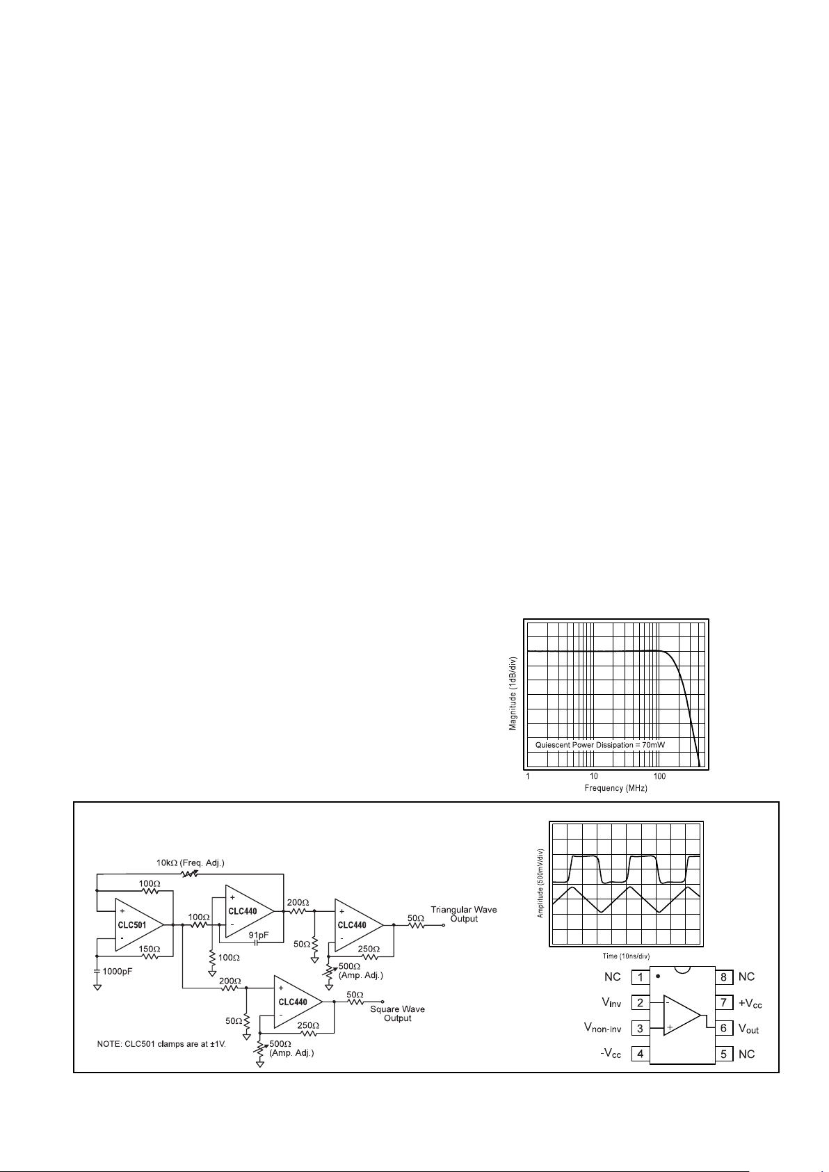
Typical Application
10MHz to 40MHz Square and Triangular Wave Generator
Pinout
DIP & SOIC
General Description
The CLC440 is a wideband, low-power, voltage feedback op amp
that offers 750MHz unity-gain bandwidth, 1500V/µs slew rate, and
90mA output current. For video applications, the CLC440 sets new
standards for voltage f eedback monolithics b y off ering the impressive combination of 0.015% differential gain and 0.025° differential phase errors while dissipating a mere 70mW.
The CLC440 incorporates the proven properties of Comlinear’s
current feedback amplifiers (high bandwidth, f ast sle wing, etc.) into a
“classical” voltage feedback architecture. This amplifier possesses
truly differential and fully symmetrical inputs both having a high
900kΩ impedance with matched low input bias currents.
Furthermore, since the CLC440 incorporates voltage feedback, a
specific R
f
is not required for stability. This flexibility in choosing R
f
allows for numerous applications in wideband filtering and integration.
Unlike several other high-speed voltage feedback op amps, the
CLC440 operates with a wide range of dual or single supplies
allowing for use in a multitude of applications with limited supply
availability. The CLC440’s low 3.5nV/√Hz(en) and 2.5pA/√Hz(in)
noise sets a very low noise floor.
CLC440
High-Speed, Low-Power,Voltage Feedback Op Amp
N
June 1999
CLC440
High-Speed, Low-Power, Voltage Feedback Op Amp
Generator Waveforms
© 1999 National Semiconductor Corporation http://www.national.com
Printed in the U.S.A.
Page 2

PARAMETERS CONDITIONS TYP MIN/MAX RATINGS UNITS NOTES
Ambient T emper ature CLC440 +25˚C +25˚C 0 to 70˚C -40 to 85˚C
FREQUENCY DOMAIN RESPONSE
-3dB bandwidth A
V
=+2 V
out
< 0.2V
pp
260 165 165 135 MHz
V
out
< 4.0V
pp
190 150 135 130 MHz
-3dB bandwidth A
V
=+1 V
out
< 0.2V
pp
750 MHz
gain bandwidth product V
out
< 0.2V
pp
230 MHz
gain flatness
V
out
< 2.0VppDC to 75MHz
0.05 0.15 0.20 0.20 dB
linear phase deviation
V
out
< 2.0VppDC to 75MHz
0.8 1.2 1.5 1.5 deg
differential gain 4.43MHz, R
L
=150Ω 0.015 0.03 0.04 0.04 %
differential phase 4.43MHz, R
L
=150Ω 0.025 0.05 0.06 0.06 deg
TIME DOMAIN RESPONSE
rise and fall time 2V step 1.5 2.0 2.2 2.5 ns
4V step 3.2 4.2 4.5 5.0 ns
settling time to 0.05% 2V step 10 14 16 16 ns
overshoot 4V step 7 13 13 13 %
slew rate 4V step, ±0.5V crossing 1500 900 750 600 V/µs
DISTORTION AND NOISE RESPONSE
2nd harmonic distortion 2V
pp
, 5MHz -64 -59 -59 -59 dBc
2V
pp
, 20MHz -52 -46 -46 -46 dBc
3rd harmonic distortion 2V
pp
, 5MHz -70 -65 -64 -64 dBc
2V
pp
, 20MHz -51 -45 -43 -43 dBc
equivalent input noise
voltage >1MHz 3.5 4.5 5.0 5.0 nV/√Hz
current >1MHz 2.5 3.5 4.0 4.0 pA/√Hz
STATIC DC PERFORMANCE
input offset voltage 1.0 3.0 3.5 4.0 mV A
average drift 5.0 10 10 µV/°C
input bias current 10 30 35 40 µAA
average drift 30 50 60 nA/°C
input offset current 0.5 2.0 2.0 3.0 µAA
average drift 3.0 10 10 nA/°C
power supply rejection ratio DC 65 58 58 58 dB
common-mode rejection ratio DC 80 65 60 60 dB
supply current R
L
= ∞ 7.0 7.5 8.0 8.0 mA A
MISCELLANEOUS PERFORMANCE
input resistance common-mode 900 500 400 300 kΩ
input capacitance common-mode 1.2 2.0 2.0 2.0 pF
differential-mode 0.5 1.0 1.0 1.0 pF
input voltage range common-mode ±3.0 ±2.8 ±2.7 ±2.7 V
output voltage range R
L
= 100Ω ±2.5 ±2.3 ±2.2 ±2.2 V
output voltage range R
L
= ∞ ±3.0 ±2.8 ±2.7 ±2.7 V
output current ±80 ±72 ±65 ±45 mA
Min/max ratings are based on product characterization and simulation. Individual parameters are tested as noted. Outgoing quality levels are
determined from tested parameters.
CLC440 Electrical Characteristics
(AV= +2, Rf= Rg= 250Ω:Vcc= + 5V, RL= 100Ω unless specified)
Absolute Maximum Ratings
voltage supply
±
6V
I
out
is short circuit protected to ground
common-mode input voltage
±
Vcc
maximum junction temperature +150˚C
storage temperature range -65˚C to +150˚C
lead temperature (soldering 10 sec) +300˚C
ESD rating (human bodey model) <1000V
Notes
A) J-level: spec is 100% tested at +25˚C.
Transitor Count 46
Ordering Information
Model Temperature Range Description
CLC440AJP -40˚C to +85˚C 8-pin PDIP
CLC440AJE -40˚C to +85˚C 8-pin SOIC
CLC440A8B -55˚C to +125˚C 8-pin hermetic CerDIP,
MIL-STD-883
Contact factory for SMD number.
Pac kage Thermal Resistance
Package
θθ
jc
θθ
ja
Plastic (AJP) 70˚/W 125˚/W
Surface Mount (AJE) 60˚/W 140˚/W
CerDip 40˚/W 130˚/W
http://www.national.com 2
Page 3
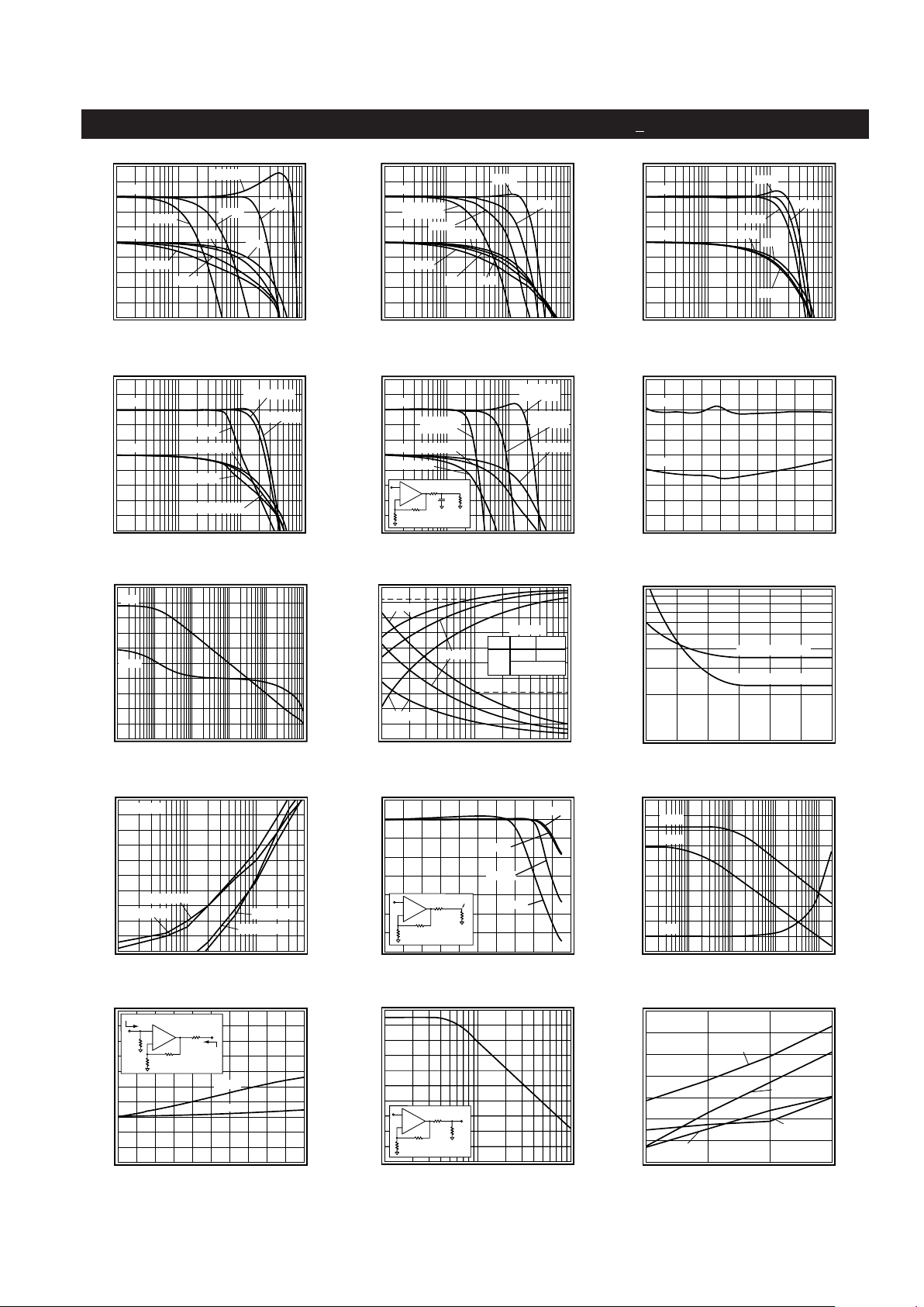
CLC440 Typical Performance Characteristics
(AV= +2, Rf= 250Ω:Vcc= + 5V, RL= 100Ω unless specified)
Non-Inverting Frequency Response
Magnitude (1dB/div)
Phase (deg)
-180
-90
-135
-45
0
1
10
100
Frequency (MHz)
AV = 10
AV = 2
AV = 1
AV = 1(Rf = 0)
AV = 2
AV = 10
AV = 5
AV = 5
1000
Gain
Phase
Inverting Frequency Response
Magnitude (1dB/div)
Phase (deg)
-360
-270
-315
-225
-180
1
10
100
Frequency (MHz)
AV -10
AV -1
A
V
-2
AV = -1
AV = -2
AV = -10
(Rf = 500Ω)
AV = -5
AV -5
1000
Gain
Phase
Frequency Response vs. Load
Magnitude (1dB/div)
Phase (deg)
-180
-90
-135
-45
0
1
10
100
Frequency (MHz)
RL=1K
R
L
=100
RL=1K
RL=100
RL=50
RL=50
1000
Gain
Phase
Frequency Response vs. V
out
Magnitude (1dB/div)
Phase (deg)
-180
-90
-135
-45
0
1
10
100
Frequency (MHz)
V
out
= 200mV
pp
1000
Gain
Phase
V
out
= 2V
pp
V
out
= 5V
pp
V
out
= 5V
pp
V
out
= 200mV
pp
V
out
= 2V
pp
Frequency Response vs. Capacitive Load
Magnitude (1dB/div)
Phase (deg)
-180
-90
-135
-45
0
1
10
100
Frequency (MHz)
CL = 10pF
Rs = 50
1000
Gain
Phase
CL = 100pF
Rs = 30
CL = 1000pF
Rs = 5
CL = 1000pF
CL = 100pF
CL = 10pF
+
-
R
s
1k
C
L
Gain Flatness and Linear Phase
Magnitude (0.05dB/div)
Phase (1.0deg/div)
0
Frequency (7.5MHz/div)
75
Gain
Phase
Open Loop Gain and Phase
Open Loop Gain (dB)
Phase (deg)
1k
Frequency (Hz)
100M
Gain
Phase
10k
100k 1M
10M
80
60
40
20
0
-20
0
-90
-180
-270
BW vs. Gain for Transimpedance Configuration
C
f
(pF)
100
1000
10000
R
f
0
4
8
16
20
Bandwidth (MHz)
400
320
240
80
0
12
160
Cd = 1pF
Cd = 5pF
Cd = 20pF
BW
C
f
R
f
1000
C
f
1.6 BW123
See dashed lines
Example
Equivalent Input Noise
Noise Voltage (nV/√Hz)
Frequency (Hz)
10
1
1k
100
10k
100k
1M
10M
Noise Current (pA/√Hz)
10
1
Voltage = 3.5nV/√Hz
Current = 2.5pA/√Hz
100M
Harmonic Distortion vs. Frequency
Distortion (dBc)
Frequency (MHz)
-45
-55
-95
0.1
1
10
-75
-85
-65
3rd RL = 100
2nd RL = 1k
3rd RL = 1k
2nd RL = 100
50
Vo = 2V
pp
1dB Compression
Gain (1dB/div)
Output Power (P
out
)
-4
0
16
50MHz
100MHz
5MHz
20MHz
4812
+
-
50Ω
50Ω
Pout
250Ω
250Ω
Input and Output VSWR
VSWR
Frequency (20MHz/div)
0
200
Input
Output
1.0
1.4
1.8
2.2
40 80 120 160
+
-
50Ω
Output
50Ω
250Ω
50Ω
Input
PSRR, CMRR, and Closed Loop R
out
PSRR/CMRR (dB)
Frequency (Hz)
45
35
10k
100k
100M
15
25
100
80
40
0
60
5
1M 10M
20
CMRR
R
out
PSRR
R
out
(Ω)
Differential Gain and Phase
Differential Gain (%), Phase (deg)
Number of 150Ω Loads
0.12
1
2
3
0.04
0
0.08
Gain
Positive Sync
Phase
Negative Sync
4
Gain
Negative Sync
Phase
Positive Sync
2-Tone, 3rd Order Intermodulation Intercept
Intercept Point (+dBm)
1
10
100
Frequency (MHz)
50
40
30
20
10
0
+
-
50Ω
P
out
250Ω
250Ω
50Ω
3 http://www.national.com
Page 4

General Design Equations
The CLC440 is a unity gain stable voltage feedback
amplifier.The matched input bias currents track well over
temperature. This allows the DC offset to be minimized
by matching the impedance seen by both inputs.
Gain
The non-inverting and inverting gain equations for the
CLC440 are as follows:
Non-inverting Gain:
Inverting Gain:
Gain Bandwidth Product
The CLC440 is a voltage feedback amplifier, whose
closed-loop bandwidth is approximately equal to the
gain-bandwidth product (GBP) divided by the gain (Av).
For gains greater than 5, Av sets the closed-loop bandwidth of the CLC440.
Closed Loop Bandwidth =
GBP = 230MHz
For gains less than 5, refer to the frequency response
plots to determine maximum bandwidth.
Output Drive and Settling Time Performance
The CLC440 has large output current capability. The
90mA of output current makes the CLC440 an excellent
choice for applications such as:
•
Video Line Drivers
•
Distribution Amplifiers
When driving a capacitive load or coaxial cable, include a
series resistance Rsto back match or improve settling
time. Refer to the “Settling Time vs .Capacitive Load”plot
in the typical performance section to determine the
recommended resistance for various capacitive loads.
When driving resistive loads of under 500Ω, settling time
performance diminishes. This degradation occurs
because a small change in voltage on the output causes
a large change of current in the power supplies. This
current creates ringing on the power supplies. A small
resistor will dampen this effect if placed in series with the
6.8µF bypass capacitor.
Noise Figure
Noise Figure (NF) is a measure of noise degradation
caused by an amplifier.
where,
eni= Total Equivalent Input Noise Density
Due to the Amplifier
et= Thermal Voltage Noise (
seq
)
CLC440 Typical Performance Characteristics
(AV= +2, Rf= 250Ω:Vcc= + 5V, RL= 100Ω unless specified)
Ib and Ios vs. Common-Mode Voltage
Offset Current, I
os
(5nA/div)
Bias Current, I
b
(0.5µA/div)
Common-Mode Input Voltage (V)
-4.0
-2.4
2.4
0
4.0
0
-0.8 0.8
I
b
l
os
-10
-20
10
20
2.0
1.0
-1.0
-2.0
APPLICATION INFORMATION
Pulse Response
Output Voltage (0.5V/div)
Time (5ns/div)
2.0
1.0
-1.0
-2.0
0
AV = +2
AV = -2
0.05% Settling Time vs. Capacitive Load
Settling Time, T
s
(ns) to 0.05%
10
100
1000
Load Capacitance CL (pF)
80
60
40
20
0
Recommended R
s
(Ω)
55
45
35
25
15
+
-
R
s
1k
C
L
R
s
T
s
Short Term Settling Time
Settling Error % of Output Step
Time (ns
)
0
20
80
0.1
10040 60
0.2
0
-0.1
-0.2
Long Term Settling Time
Settling Error % of Output Step
Time (s
)
10
-9
10
-7
10
-1
0.1
10
0
10-510
-3
0.2
0
-0.1
-0.2
10
-2
10
-4
10
-6
10
-8
1
R
R
f
g
+
−
R
R
f
g
GBP
A
v
A
RR
R
v
f
g
g
=
+
()
NF 10LOG
S/N
S/N
10LOG
e
e
ii
oo
ni
2
t
2
=
=
4kTR
Typical DC Errors vs. Temperature
Input Offset Voltage, V
io
(mV)
Input Bias, Offset Current, l
b
l
os
(µA)
Temperature (C°)
0.4
0
-60
-20
100
-0.8
-1.6
-0.4
140
6
2
-6
-14
-2
-1.2
20 60
-10
l
os
l
b
V
io
http://www.national.com 4
Page 5

Figure 1 shows the noise model for the non-inverting
amplifier configuration. The model includes all of the
following noise sources:
•
Input voltage noise (en)
•
Input current noise (in= in+= in-)
•
Thermal Voltage Noise (et) associated with each
external resistor
Figure 1: Non-inverting Amplifier Noise Model
The total equivalent input noise density is calculated
by using the noise model shown. Equations 1 and 2
represent the noise equation and the resulting equation
for noise figure.
Equation 1: Noise Equation
Equation 2: Noise Figure Equation
The noise figure is related to the equivalent source
resistance (R
seq
) and the parallel combination of Rfand
Rg.To minimize noise figure, the following steps are
recommended:
•
Minimize RfIIR
g
•
Choose the optimum Rs(R
OPT
)
R
OPT
is the point at which the NF curve reaches a
minimum and is approximated by:
Figure 2 is a plot of NF vs Rswith Rf= 0, Rg= ∞ (Av= +1).
The NF curves for both Unterminated and Terminated
systems are shown. The Terminated curve assumes R
s
= RT. The table indicates the NF for v arious source resistances including Rs= R
OPT
.
Layout Considerations
A proper printed circuit layout is essential for achieving
high frequency performance. National provides
evaluation boards for the CLC440 (CLC730055-DIP,
CLC730060-SOIC) and suggests their use as a guide for
high frequency layout and as an aid in device testing and
characterization.
Figure 2: Noise Figure vs. Source Resistance
These boards were laid out for optimum, high-speed
performance. The ground plane was removed near the
input and output pins to reduce parasitic capacitance.
And all trace lengths were minimized to reduce series
inductances.
Supply bypassing is required for the amplifiers
performance. The bypass capacitors provide a low
impedance return current path at the supply pins. They
also provide high frequency filtering on the power supply
traces. 6.8µF tantalum, 0.01µF ceramic, and 500pF
ceramic capacitors are recommended on both supplies.
Place the 6.8µF capacitors within 0.75 inches of the
power pins, and the 0.01µF and 500pF capacitors less
than 0.1 inches from the power pins.
Dip sockets add parasitic capacitance and inductance
which can cause peaking in the frequency response and
overshoot in the time domain response. If sockets are
necessary, flush-mount socket pins are recommended.
The device holes in the 730055 evaluation board are
sized for Cambion P/N 450-2598 socket pins, or their
functional equivalent.
Transimpedance Amplifier
The low 2.5pA/√Hz input current noise and unity gain
stability make the CLC440 an excellent choice for
transimpedance applications. Figure 3 illustrates a
low noise transimpedance amplifier that is commonly
implemented with photo diodes. Rfsets the transimpedance gain. The photo diode current multiplied by R
f
determines the output voltage.
Figure 3: Transimpedance Amplifier Configuration
R
seq
R
f
+
-
R
g
CLC440
*
i
n+
*
*
e
n
i
n-
*
*
*
4kTR
seq
4kTR
f
4kTR
g
R
seq
= Rs for Unterminated Systems
R
seq
= Rs II RT for Terminated Systems
Noise Figure vs. Source Resistance
Noise Figure (dB)
Source Resistance (Ω)
10
100k
Unterminated
Terminated
10
15
20
25
100 1k 10k
5
0
R
opt
= 2800Ω
R
opt
= 1400Ω
Rs(Ω)
50
R
OPT
NF Unterminated
12.03dB
3.13dB
NF Terminated
17.90dB
6.15dB
Applications Circuits
I
in
-
+
CLC440
C
d
R
f
C
f
Photo Diode
Representation
V
out
= -I
in
*
R
f
V
out
e e i R R IIR 4kTR 4kT R IIR
ni
n2n2seq
2
f
g
2
seq
f
g
=+ +
()
++
()
NF 10LOG
e i R RIIR 4kTR 4kT R IIR
4kTR
n2n2seq
2
f
g
2
seq
f
g
seq
=
++
()
++
()
R
e
i
OPT
n
n
≅
5 http://www.national.com
Page 6

The capacitances are defined as:
•
Cin= Internal Input Capacitance of the CLC440
(typ 1.2pF)
•
Cd= Equivalent Diode Capacitance
•
Cf= Feedback Capacitance
The transimpedance plot in the typical performance
section provides the recommended Cfand expected
bandwidth for different gains and diode capacitances.
The feedback capacitances indicated on the plot
give optimum gain flatness and stability. If a smaller
capacitance is used, then peaking will occur. The
frequency response shown in Figure 4 illustrates the
influence of the feedback capacitance on gain flatness.
Figure 4
The total input current noise density (ini) for the basic
transimpedance configuration is shown in Equation 3.
The plot of current noise density versus feedback
resistance is shown in Figure 5.
Figure 5
Equation 3:Total Equivalent Input Referred Current
Noise Density
Rectifier
The large bandwidth of the CLC440 allows for high speed
rectification. A common rectifier topology is shown in
Figure 6. R1and R2set the gain of the rectifier. V
out
for
a 5MHz, 2Vppsinusoidal input is shown in Figure 7.
Figure 6: Rectifier Topology
Figure 7: Rectifier Output
Tunable Low Pass Filter
The center frequency of the low pass filter (LPF) can be
adjusted by varying the CLC522 gain control voltage, Vg.
Figure 8: Tunable Low Pass Filter
Transimpedance Amplifier
Frequency Response
Gain (dB)
Frequency (Hz)
10k
1M
40
60
100k
30
20
50
70
80
10M 100M 1G
I
in
-
+
CLC440
5
pF
1k
C
f
100Ω
Cf = 0
C
f
= 1pF
C
f
= 2pF
C
f
= 5pF
Cf = 2.5pF
Current Noise Density vs.
Feedback Resistance
Current Noise Density (pA/√Hz)
Feedback Resistance (kΩ)
0.1
10
i
ni
10
15
20
25
1.0
5
0
30
35
40
i
f
i
n
e
n
R
f
(Total)
V
in
-
+
CLC440
R
2
R
1
D
2
D
1
V
out
Rectifier Output
V
out
(V)
Time (ns)
0
200
-1.2
-0.8
-0.4
0.4
100
-1.6
-2.0
0
0.8
1.2
2.0
300 400 500
1.6
Qk
RC
RR CC
2
1212
=
V
in
-
+
CLC440
R
R
2
R
T
V
out
C
2
-
+
CLC440
-
+
CLC522
R
1
C
1
R
in
R
g
R
a
R
f
20Ω
V
g
ω
o
1212
k
RRCC
=
R
V
1.8mA
g
in (max)
=
A k 1.85
R
R
v (max)
f
g
==
ii
e
R
4kT
R
ni
n
n
2
f
2
f
=+
+
http://www.national.com 6
Page 7

This page intentionally left blank.
7 http://www.national.com
Page 8

CLC440
High-Speed, Low-Power, Voltage Feedback Op Amp
http://www.national.com 8
Customer Design Applications Support
National Semiconductor is committed to design excellence. For sales, literature and technical support, call the
National Semiconductor Customer Response Group at 1-800-272-9959 or fax 1-800-737-7018.
Life Support Policy
National’s products are not authorized for use as critical components in life support devices or systems without the express written approval of
the president of National Semiconductor Corporation. As used herein:
1. Life support devices or systems are devices or systems which, a) are intended for surgical implant into the body, or b) support or
sustain life, and whose failure to perform, when properly used in accordance with instructions for use provided in the labeling, can
be reasonably expected to result in a significant injury to the user.
2. A critical component is any component of a life support device or system whose failure to perform can be reasonably expected to
cause the failure of the life support device or system, or to affect its safety or effectiveness.
National Semiconductor National Semiconductor National Semiconductor National Semiconductor
Corporation Europe Hong Kong Ltd. Japan Ltd.
1111 West Bardin Road Fax:(+49) 0-180-530 85 86 2501 Miramar Tower Tel: 81-043-299-2309
Arlington, TX 76017 E-mail:europe.suppor t.nsc.com 1-23 Kimberley Road Fax: 81-043-299-2408
Tel: 1(800) 272-9959 Deutsch Tel: (+49) 0-180-530 85 85 Tsimshatsui, Kowloon
Fax:1(800) 737-7018 English Tel: (+49) 0-180-532 78 32 Hong Kong
Francais Tel: (+49) 0-180-532 93 58 Tel: (852) 2737-1600
Italiano Tel: (+49) 0-180-534 16 80 Fax: (852) 2736-9960
National does not assume any responsibility for use of any circuitry described, no circuit patent licenses are implied and National reserves the right at any time without notice to change said
circuitry and specifications.
N
 Loading...