

Datasheet CLC430MDC, CLC430AWG-MPR, CLC430AJP, CLC430AJE-TR13, CLC430AJE Datasheet (NSC)
...Page 1
N
CLC430
General Purpose 100MHz Op Amp with Disable
General Description
The CLC430 is a low-cost, wideband monolithic amplifier for general
purpose applications. The CLC430 utilizes National’s patented
current feedback circuit topology to provide an op amp with a slew rate
of 2000V/µs, 100MHz unity-gain bandwidth and fast output disable
function. Like all current feedback op amps, the CLC430 allows the
frequency response to be optimized (or adjusted) by the selection of
the feedback resistor. For demanding video applications, the 0.1dB
bandwidth to 20MHz and differential gain/phase of 0.03%/0.05° make
the CLC430 the preferred component for broadcast quality NTSC and
PAL video systems.
The large voltage swing (28Vpp), continuous output current (85mA)
and slew rate (2000V/µs) provide high-fidelity signal conditioning for
applications such as CCDs, transmission lines and low impedance
circuits. Even driving loads of 100Ω, the CLC430 provides very low
2nd and 3rd harmonic distortion at 1MHz (-76/-82dBc).
Video distribution, multimedia and general purpose applications will
benefit from the CLC430’s wide bandwidth and disable feature. Power
is reduced and the output becomes a high impedance when disabled.
The wide gain range of the CLC430 makes this general purpose op
amp an improved solution for circuits such as active filters, differential-to-single-ended drivers, DAC transimpedance amplifiers and
MOSFET drivers.
June 1999
Features
■ 0.1dB gain flatness to 20MHz (A
v
=+2)
■ 100MHz bandwidth (A
v
=+1)
■ 2000V/µs slew rate
■ 0.03%/0.05° differential gain/phase
■ ±5V, ±15V or single supplies
■ 100ns disable to high-impedance output
■ Wide gain range
■ Low cost
Applications
■ Video distribution
■ CCD clock driver
■ Multimedia systems
■ DAC output buffers
■ Imaging systems
CLC430
General Purpose 100MHz Op Amp with Disable
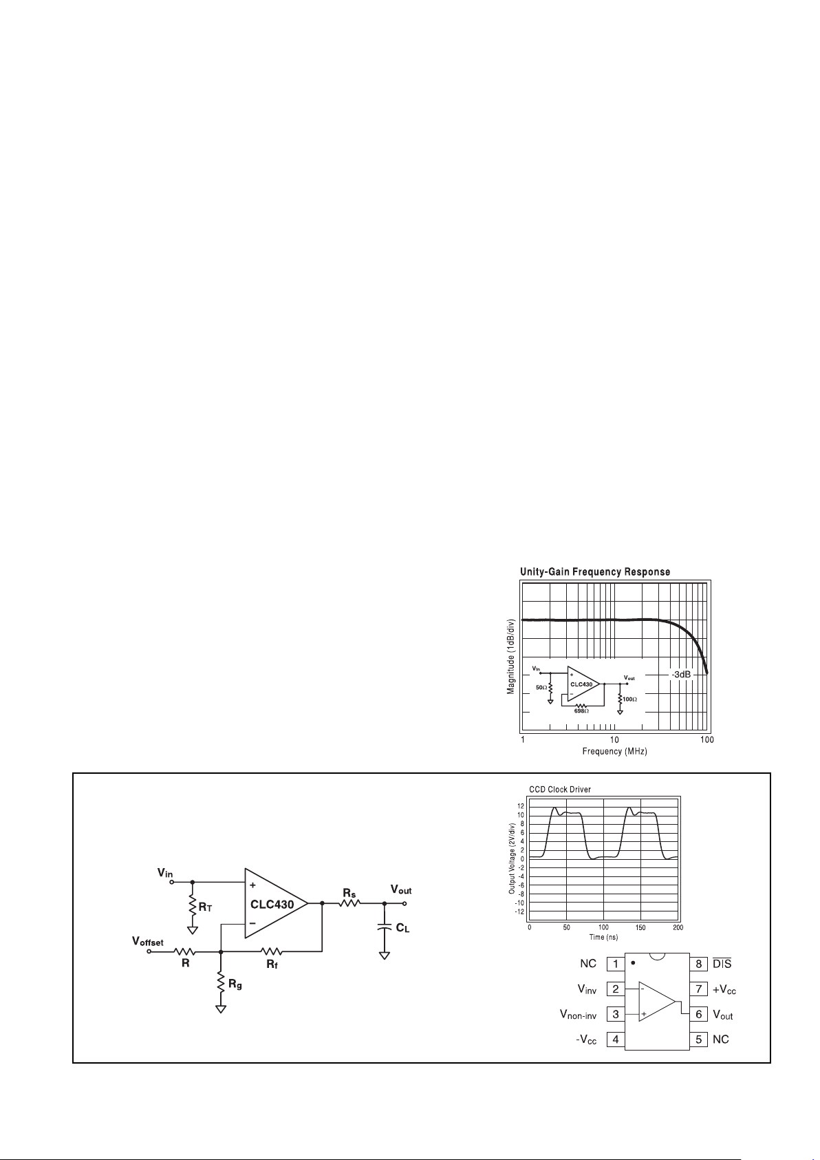
Pinout
DIP & SOIC
Typical Application
CCD Clock Driver
1999 National Semiconductor Corporation http://www.national.com
Printed in the U.S.A.
Page 2
CLC430 Electrical Characteristics (V
CC
= ±15V; A
V
= +2V/V; R
f
=604
ΩΩ
ΩΩ
Ω; R
L
= 100
ΩΩ
ΩΩ
Ω; unless noted)
PARAMETERS CONDITIONS V
cc
TYP MIN/MAX RATINGS UNITS NOTES
Ambient Temperature CLC430 25°C 25°C 0 to 70°C -40 to 85°C
FREQUENCY DOMAIN RESPONSE
unity-gain bandwidth V
out
< 1.0V
pp
±15 100 MHz
small-signal bandwidth V
out
< 1.0V
pp
±15 75 50 45 42 MHz
V
out
< 1.0V
pp
±5 55 35 MHz
0.1dB bandwidth V
out
< 1.0V
pp
±15 2 0 7 MHz
V
out
< 1.0V
pp
±5 16 MHz
large-signal bandwidth V
out
= 10V
pp
30 22 20 19 MHz
gain flatness V
out
< 1.0V
pp
peaking DC to 10MHz 0.0 0.1 0.2 0.2 dB
rolloff DC to 20MHz 0.1 0.7 1.0 1.2 dB
linear phase deviation DC to 20MHz 0.5 1.8 2.0 2.1 °
differential gain 4.43MHz, R
L
=150Ω ±15 0.03 0.05 0.06 0.06 %
4.43MHz, R
L
=150Ω ±5 0.03 0.05 %
differential phase 4.43MHz, RL=150Ω ±15 0.05 0.09 0.12 0.13 °
4.43MHz, R
L
=150Ω ±5 0.09 0.19 °
TIME DOMAIN RESPONSE
rise and fall time 2V step 5 7 7 7 n s
10V step 10 1 4 1 4 14 ns
settling time to 0.05% 2V step 35 5 0 5 5 5 5 ns
overshoot 2V step 5 15 1 5 15 %
slew rate 20V step 20 00 1500 1450 1450 V/µs
DISTORTION AND NOISE RESPONSE
2
nd
harmonic distortion 1Vpp,1MHz, RL=500 -89 dBc
3
rd
harmonic distortion 1Vpp,1MHz, RL=500 -92 dBc
input voltage noise >1MHz 3.0 3.5 3.7 3.8 nV/√Hz
non-inverting input current noise >1MHz 3.2 6.0 6.3 6.8 pA/√Hz
inverting input current noise >1MHz 15 18 20 21 pA/√Hz
DC PERFORMANCE
input offset voltage ±15 1.0 7.5 9.0 10.0 mV A
average drift 25 --- 50 5 0 µV/ C
input bias current non-inverting ±15,±5 3 14 16 20 µAA
average drift 10 --- 100 1 00 nA/°C
input bias current inverting ±15,±5 3 14 15 17 µAA
average drift 10 --- 60 9 0 nA/°C
power-supply rejection ratio DC 62 56 54 53 dB
common-mode rejection ratio DC 62 54 5 3 5 2 dB
supply current R
L
= ∞ ±15,±5 11, 8.5 12 13 14.5 mA A
disabled R
L
= ∞ ±15,±5 1.5 2.0 2.2 2.4 mA A
SWITCHING PERFORMANCE
turn on time 2 0 0 300 320 340 ns
turn off time (Note 2) 100 200 200 200 ns
off isolation 10MHz 59 5 6 56 56 dB
high input voltage V
IH
±15 11.8 12.5 12.7 V
±5 1.8 2.5 2.7 V
low input voltage V
IL
±15 10.8 10.5 10.0 V
±5 0.8 0.6 0.1 V
MISCELLANEOUS PERFORMANCE
Non-inverting input resistance 8.0 3.0 2.5 1.7 MΩ
Non-inverting input capacitance 0.5 1.0 1.0 1.0 pF
input voltage range common mode ±15 ±12.5 ±12.3 ±12.1 ±11.8 V
common mode ±5 ±2.5 ±2.3 ±2.2 ±1.9 V
output voltage range R
L
= ∞ ±15 ±14 ±13.7 ±13.7 ±13.6 V
RL= ∞ ±5 ±4.0 ±3.9 ±3.8 ±3.7 V
output current ±85 ± 60 ± 50 ± 45 mA
Min/max ratings are based on product characterization and simulation. Individual parameters are tested as noted. Outgoing quality levels
are determined from tested parameters.
http://www.national.com 2
Absolute Maximum Ratings
supply voltage ±16.5V
short circuit current (note 1)
common-mode input voltage ±V
cc
maximum junction temperature +150°C
storage temperature -65°C to+150°C
lead temperature (soldering 10 sec) +300°C
ESD rating (human body model) 4000V
Notes
A) J-level: spec is 100% tested at +25°C.
1)Output is short circuit protected to ground, however
maximum reliability is obtained if output current does not
exceed 125mA.
2) To>50dB attenuation @ 10MHz.
Page 3
3 http://www.national.com
Page 4

http://www.national.com 4
Model Temperature Range Description
CLC430AJP -40°C to +85°C 8-pin PDIP
CLC430AJE -40°C to +85°C 8-pin SOIC
CLC430A8B -55°C to +125°C 8-pin CERDIP, MIL-STD-883
DESC SMD number: 5962-92030.
Ordering Information
Reliability Information
Transistor count 38
Package Thermal Resistance
Package
θθ
θθ
θ
JC
θθ
θθ
θ
JA
AJP 60°C/W 115°C/W
AJE 55°C/W 135°C/W
A8B 30°C/W 120°C/W
Page 5

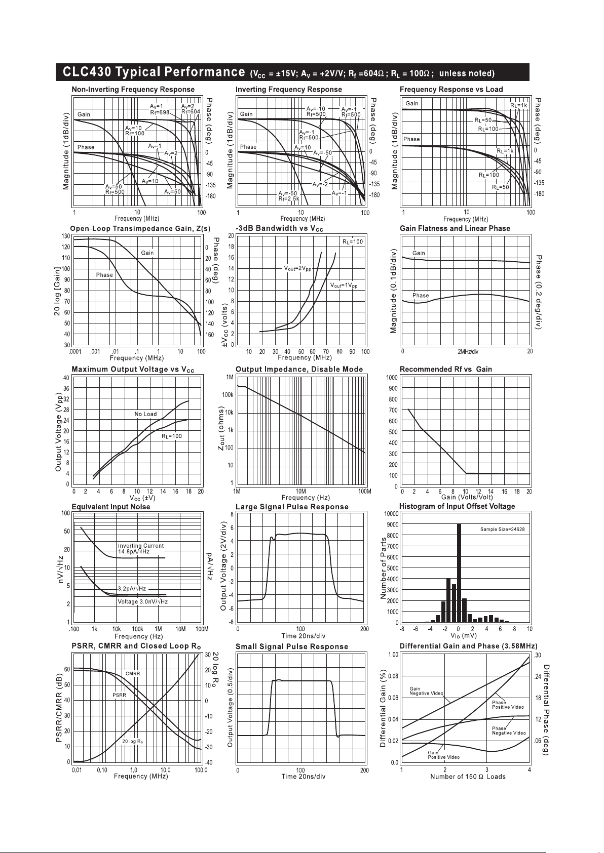
General Design Considerations
The CLC430 is a general purpose current-feedback amplifier for use in a variety of small- and large-signal applications. Use the feedback resistor to fine tune the gain
flatness and -3dB bandwidth for any gain setting. Comlinear provides information for the performance at a gain of
+2 for small and large signal bandwidths. The plots show
feedback resistor values for selected gains.
Gain
Use the following equations to set the CLC430's noninverting or inverting gain:
Non-Inverting Gain = 1+
R
R
f
g
Inverting Gain = -
R
R
f
g
Choose the resistor values for non-inverting or inverting
gain by the following steps.
V
in
V
out
R
f
R
g
R
s
R
in
CLC430
+
-
Fig. 0 Component Identification
1) Select the recommended feedback resistor Rf (refer
to plot in the plot section entitled
Rf vs Gain
).
2) Choose the value of Rg to set gain.
3) Select Rs to set the circuit output impedance.
4) Select Rin for input impedance and input bias.
High Gains
Current feedback closed-loop bandwidth is independent of
gain-bandwidth-product for small gain changes. For larger
gain changes the optimum feedback register Rf is derived
by the following:
As gain is increased, the feedback resistor allows bandwidth
to be held constant over a wide gain range. For a more
complete explanation refer to application note OA-25 Stability Analysis of Current-Feedback Amplifiers.
Resistors have varying parasitics that affect circuit performance in high-speed design. For best results, use leaded
metal-film resistors or surface mount resistors. A SPICE
model for the CLC430 is available to simulate overall
circuit performance.
Enable / Disable Function
The CLC430 amplifier features an enable/disable function
that changes the output and inverting input from low to high
impedance. The pin 8 enable/disable logic levels are as
follows:
V
cc
±15V ±5V
Enable >12.7V >2.7V
Disable <10.0V <0.8V
The amplifier is enabled with pin 8 left open due to the 2kΩ
pull-up resistor, shown in Fig. 1.
T o CLC430
Bias network
2kΩ
+V
cc
Pin 8DISABLE
8kΩ
-V
cc
Fig. 1 Pin 8 Equivalent Disable Circuit
Open-collector or CMOS interfaces are recommended to
drive pin 8. The turn-on and off time depends on the speed
of the digital interface.
The equivalent output impedance when disabled is shown
in Fig. 2. With Rg connected to ground, the sum of Rf and
Rg dominates and reduces the disabled output impedance. To raise the output impedance in the disabled state,
connect the CLC430 as a unity-gain voltage follower by
removing Rg. Current-feedback op-amps need the recommended Rf in a unity-gain follower circuit. For high density
circuit layouts consider using the dual CLC431 (with
disable) or the dual CLC432 (without disable).
Equivalent Impedance
in Disable
R
f
V
out
R
g
V
in
300kΩ
8pF
+
-
Fig. 2 Equivalent Disabled Output Impedance
2nd and 3rd Harmonic Distortion
To meet low distortion requirements, recognize the effect
of the feedback resistor. Increasing the feedback resistor
will decrease the loop gain and increase distortion. Decreasing the load impedance increases 3rd harmonic
distortion more than 2nd.
Differential Gain and Differential Phase
The CLC430 has low DG and DP errors for video applications. Add an external pulldown resistor to the CLC430’s
output to improve DG and DP as seen in Fig.3. A 604Ω R
P
will improve DG and DP to 0.01% and 0.02°.
5 http://www.national.com
RA
f
v
=−⋅
()
724 60ΩΩ
Page 6

V
in
-V
cc
V
out
Add R to
improve
DG and DP
p
R
p
R
f
R
g
R
s
R
in
CLC430
+
-
Fig. 3 Improved DG and DP Video Amplifier
Printed Circuit Layout
To get the best amplifier performance careful placement of
the amplifier, components and printed circuit traces must
be observed. Place the 0.1µF ceramic decoupling capacitors less than 0.1" (3mm) from the power supply pins.
Place the 6.8µF tantalum capacitors less than 0.75"
(20mm) from the power supply pins. Shorten traces
between the inverting pin and components to less than
0.25" (6mm). Clear ground plane 0.1" (3mm) away from
pads and traces that connect to the inverting, noninverting and output pins. Do not place ground or power
plane beneath the op-amp package. Comlinear provides
literature and evaluation boards 730013 DIP or 730027
SOIC illustrating the recommended op-amp layout.
Applications Circuits
Level Shifting
The circuit shown in Fig. 4 implements level shifting by AC
coupling the input signal and summing a DC voltage. The
resistor Rin and the capacitor C set the high-pass break
frequency. The amplifier closed-loop bandwidth is fixed by
the selection of Rf. The DC and AC gains for circuit of Fig.
4 are different. The AC gain is set by the ratio of Rf and Rg.
And the DC gain is set by the parallel combination of R
g
and R2.
C
V
in
DC
V
in
AC
V
out
R
f
R
g
R
2
R
in
+
-
CLC430
Fig. 4 Level Shifting Circuit
Multiplexing
Multiple signal switching is easily handled with the disable
function of the CLC430. Board trace capacitance at the
output pin will affect the frequency response and switching
transients. To lessen the effects of output capacitance
place a resistor (Ro) within the feedback loop to isolate the
outputs as shown in Fig. 5. To match the mux output
impedance to a transmission line, add a resistor (Rs) in
series with the output.
R
f
R
f
R
s
R
o
R
o
R
in
R
in
R
L
R
g
R
g
V
out
V
in1
V
in2
DIS1
DIS2
CLC430
CLC430
Fig. 5 Output Connection
Automatic Gain Control
Current-feedback amplifiers can implement very fast
automatic-gain control circuits. The circuit shown in Fig.
6 shows an AGC circuit using the CLC430, a half-wave
rectifier, an integrator and a FET. The CLC430 currentfeedback amplifier maintains constant bandwidth and
linear phase over AGC's gain range. This circuit effectively
controls the output level for continuous signals.
Fig. 6 AGC Circuit
The bandwidth of the CLC430 AGC is limited by Rf , the
feedback resistor. The FET gate voltage is limited to a
range of:
R of 750Ω and C1 of 1.0µF gives a useful Rds range of
approximately 150 to 2K ohms. Scaling the integrator gain
or adding attenuation before the diode D accommodates
large signal swings. Determine the overall gain by:
The integrator sets the loop time constant.
−< <−
25 1
.V
g
1+
+
R
RR
f
gds
VV
R
R
V
R
R
out in
f
g
in
f
ac
DC
=+
−
1
22
||R
http://www.national.com 6
Page 7

This page intentionally left blank.
7 http://www.national.com
Page 8

CLC430
General Purpose 100MHz Op Amp with Disable
http://www.national.com
8
Customer Design Applications Support
National Semiconductor is committed to design excellence. For sales, literature and technical support, call the
National Semiconductor Customer Response Group at 1-800-272-9959 or fax 1-800-737-7018.
Life Support Policy
National’s products are not authorized for use as critical components in life support devices or systems without the express written approval
of the president of National Semiconductor Corporation. As used herein:
1. Life support devices or systems are devices or systems which, a) are intended for surgical implant into the body, or b) support or
sustain life, and whose failure to perform, when properly used in accordance with instructions for use provided in the labeling, can
be reasonably expected to result in a significant injury to the user.
2. Acritical component is any component of a life support device or system whose failure to perform can be reasonably expected to
cause the failure of the life support device or system, or to affect its safety or effectiveness.
National Semiconductor National Semiconductor National Semiconductor National Semiconductor
Corporation Europe Hong Kong Ltd. Japan Ltd.
1111 West Bardin Road Fax: (+49) 0-180-530 85 86 2501 Miramar Tower Tel: 81-043-299-2309
Arlington, TX 76017 E-mail: europe.support.nsc.com 1-23 Kimberley Road Fax: 81-043-299-2408
Tel: 1(800) 272-9959 Deutsch Tel: (+49) 0-180-530 85 85 Tsimshatsui, Kowloon
Fax: 1(800) 737-7018 English Tel: (+49) 0-180-532 78 32 Hong Kong
Francais Tel: (+49) 0-180-532 93 58 Tel: (852) 2737-1600
Italiano Tel: (+49) 0-180-534 16 80 Fax: (852) 2736-9960
National does not assume any responsibility for use of any circuitry described, no circuit patent licenses are implied and National reserves the right at any time without notice to change said
circuitry and specifications.
 Loading...