

Page 1
N
CLC428
Dual Wideband, Low-Noise, Voltage Feedback Op Amp
General Description
The CLC428 is a very high-speed dual op amp that offers a traditional
voltage-feedback topology featuring unity-gain stability and slewenhanced circuitry. The CLC428’s ultra low noise and very low
harmonic distortion combine to form a very wide dynamic-range op
amp that operates from a single (5 to 12V) or dual (±5V) power supply.
Each of the CLC428’s closely matched channels provides a 160MHz
unity-gain bandwidth with an ultra low input voltage noise density
(2nV/√Hz). Very low 2nd/3rd harmonic distortion (-62/-72dBc) as well
as high channel-to-channel isolation (-62dB) make the CLC428 a
perfect wide dynamic-range amplifier for matched I/Q channels.
With its fast and accurate settling (16ns to 0.1%), the CLC428 is also
a excellent choice for wide-dynamic range, anti-aliasing filters
to buffer the inputs of hi-resolution analog-to-digital converters.
Combining the CLC428’s two tightly-matched amplifiers in a single
eight-pin SOIC reduces cost and board space for many composite
amplifier applications such as active filters, differential line drivers/
receivers, fast peak detectors and instrumentation amplifiers.
To reduce design times and assist in board layout, the CLC428 is
supported by an evaluation board and a SPICE simulation model
available from National Semiconductor.
June 1999
Features
■ Wide unity-gain bandwidth: 160MHz
■ Ultra-low noise: 2.0nV/√Hz
■ Low distortion: -78dBc 2nd (2MHz)
-62/-72dBc (10MHz)
■ Settling time: 16ns to 0.1%
■ Supply voltage range: ±2.5 to ±5 or
single supply
■ High output current: ±80mA
Applications
■ General purpose dual op amp
■ Low noise integrators
■ Low noise active filters
■ Diff-in/diff-out instrumentation amp
■ Driver/receiver for transmission systems
■ High-speed detectors
■ I/Q channel amplifiers
CLC428
Dual Wideband, Low-Noise, Voltage Feedback Op Amp
Pinout
DIP & SOIC
1
2
3
4
8
7
6
5
V
out
1
V
inv
1
V
non-inv
1
-Vcc
+V
cc
V
out
2
V
inv
2
V
non-inv
2
+
+
Typical Application
5-Decade Integrator
1999 National Semiconductor Corporation http://www.national.com
Printed in the U.S.A.
Page 2
CLC428 Electrical Characteristics (V
CC
= ±5V; A
V
= +2V/V; R
f
=100
ΩΩ
ΩΩ
Ω; R
g
=100
ΩΩ
ΩΩ
Ω; R
L
= 100
ΩΩ
ΩΩ
Ω; unless noted;
PARAMETERS CONDITIONS TYP MIN/MAX RATINGS UNITS NOTES
Ambient Temperature CLC428 +25°C +25°C 0 to +70°C -40 to +85°C
FREQUENCY DOMAIN RESPONSE
gain bandwidth product V
out
< 0.5V
pp
135 100 80 70 MHz
-3dB bandwidth, Av=+1 V
out
< 0.5V
pp
160 120 90 80 MHz
Av=+2 V
out
< 0.5V
pp
80 50 40 35 MHz
V
out
< 5.0V
pp
40 25 22 20 MHz
gain flatness V
out
< 0.5V
pp
peaking DC to 200MHz 0.0 0.6 0.8 1.0 d B
rolloff DC to 20MHz 0.05 0.5 0.7 0.7 dB
linear phase deviation DC to 20MHz 0.2 1.0 1.5 1.5 °
TIME DOMAIN RESPONSE
rise and fall time 1V step 5.5 7.5 9.0 10.0 ns
settling time 2V step to 0.1% 16 20 24 24 ns
overshoot 1V step 1 5 10 10 %
slew rate 5V step 500 300 275 2 50 V/µs
DISTORTION AND NOISE RESPONSE
2
nd
harmonic distortion 1Vpp,10MHz - 62 - 5 0 - 45 - 43 dBc
3rd harmonic distortion 1Vpp,10MHz - 72 -60 - 56 - 5 6 dBc
equivalent input noise
voltage 1MHz to 100MHz 2.0 2.5 2.8 2.8 nV/ √Hz
current 1MHz to 100MHz 2.0 3.0 3.6 4.6 pA/√Hz
crosstalk input referred, 10MHz - 62 - 58 - 5 8 - 5 8 dB
STATIC DC PERFORMANCE
open-loop gain 60 56 50 50 dB
input offset voltage 1.0 2.0 3.0 3.5 m V A
average drift 5 --- 15 20 µV/°C
input bias current 1.5 25 40 65 µAA
average drift 15 0 --- 600 700 nA/ °C
input offset current 0.3 3 5 5 µA
average drift 5 --- 25 50 nA/°C
power supply rejection ratio 66 60 55 55 dB
common-mode rejection ratio 63 57 52 52 dB
supply current per channel, R
L
= ∞ 11 12 13 15 mA A
MISCELLANEOUS PERFORMANCE
input resistance common-mode 500 250 125 125 kΩ
differential-mode 200 50 25 2 5 kΩ
input capacitance common-mode 2.0 3.0 3.0 3.0 pF
differential-mode 2.0 3.0 3.0 3.0 pF
output resistance closed loop 0.05 0.1 0.2 0.2 Ω
output voltage range R
L
= ∞ ± 3.8 ± 3.5 ± 3.3 ± 3.3 V
RL=100Ω ± 3.5 ± 3.2 ± 2.6 ± 1.3 V
input voltage range common mode ± 3.7 ± 3.5 ± 3.3 ± 3.3 V
output current ± 70 ± 5 0 ± 4 0 ± 20 mA
Min/max ratings are based on product characterization and simulation. Individual parameters are tested as noted. Outgoing quality levels are
determined from tested parameters.
Ordering Information
supply voltage ±7V
short circuit current (note 1)
common-mode input voltage ±V
cc
differential input voltage ±10V
maximum junction temperature +150°C
storage temperature -65°C to+150°C
lead temperature (soldering 10 sec) +300°C
Absolute Maximum Ratings
Model Temperature Range Description
CLC428AJP -40°C to +85°C 8-pin PDIP
CLC428AJE -40°C to +85°C 8-pin SOIC
CLC428A8B -55°C to +125°C 8-pin CerDIP, MIL-STD-883
DESC SMD number: 5962-94708
http://www.national.com 2
Package θ
jc
θ
jA
Plastic (AJP) 60°C/W 115°C/W
Surface Mount (AJE) 40°C/W 115°C/W
CerDIP 25°C/W 115°C/W
Pa ckage Thermal Resistance
Notes
A)J-level: spec is 100% tested at +25°C, sample tested at +85°C.
1) Output is short circuit protected to ground, however maximum
reliability is obtained if output current does not exceed 160mA.
Transistor count 104
Reliability Information
Page 3

3 http://www.national.com
Page 4

Application Discussion
Low Noise Design
Ultimate low noise performance from circuit designs using
the CLC428 requires the proper selection of
external resistors. By selecting appropriate low-valued
resistors for Rf and Rg, amplifier circuits using the CLC428
can achieve output noise that is approximately the
equivalent voltage input noise of 2.0 nV/√Hz multiplied
by the desired gain (Av).
Each amplifier in the CLC428 has an equivalent
input noise resistance which is optimum for matching
source impedances of approximately 1k. Using a
transformer, any source can be matched to achieve the
lowest noise design.
For even lower noise performance than the CLC428,
consider the CLC425 or CLC426 at 1.05 and 1.6 nV/√Hz,
respectively.
DC Bias Currents and Offset Voltages
Cancellation of the output offset voltage due to input bias
currents is possible with the CLC428. This is done by
making the resistance seen from the inverting and noninverting inputs equal. Once done, the residual output
offset voltage will be the input offset voltage (Vos) multiplied by the desired gain (Av). Comlinear Application Note
OA-7 offers several solutions to further reduce the output
offset.
Output and Supply Considerations
With ±5V supplies, the CLC428 is capable of a typical
output swing of ±3.8V under a no-load condition.
Additional output swing is possible with slightly higher
supply voltages. For loads of less than 50Ω, the output
swing will be limited by the CLC428’s output current
capability, typically 80mA.
Output settling time when driving capacitive loads can be
improved by the use of a series output resistor. See the
plot labeled "Settling Time vs. Capacitive Load" in the
Typical Performance section.
Layout
Proper power supply bypassing is critical to insure good high
frequency performance and low noise. De-coupling capacitors of 0.1µF should be place as close as possible to the
power supply pins. The use of surface mounted capacitors
is recommended due to their low series inductance.
A good high frequency layout will keep power supply and
ground traces away from the inverting input and output
pins. Parasitic capacitance from these nodes to ground
causes frequency response peaking and possible circuit
oscillation. See OA-15 for more information. National
suggests the CLC730038 (through-hole) or the CLC730036
(SOIC) dual op amp evaluation board as a guide for high
frequency layout and as an aid in device evaluation.
http://www.national.com 4
Page 5

Analog Delay Circuit (All-Pass Network)
The circuit in Figure 1 implements an all-pass network using
the CLC428. A wide bandwidth buffer (CLC111) drives the
circuit and provides a high input impedence for the source.
As shown in Figure 2, the circuit provides a
Figure 1
Figure 2
13.1ns delay (with R =40.2Ω, C=47pF). Rf and Rg should
be of equal and low value for parasitic insensitive operation. The circuit gain is +1 and the delay is determined by
the following equations.
τ
delay d
RC T
=+
22
ch
Eq. 1
T
d
df
d
=
1
360
φ
; Eq. 2
where Td is the delay of the op amp at AV=+1. The CLC428
provides a typical delay of 2.8ns at its -3dB point.
Full Duplex Digital or Analog Transmission
Simultaneous transmission and reception of analog or
digital signals over a single coaxial cable or twisted-pair
line can reduce cabling requirements. The CLC428's wide
bandwidth and high common-mode rejection in a differential amplifier configuration allows full duplex transmission
of video, telephone, control and audio signals.
In the circuit shown in Figure 3, one of the CLC428's amps
is used as a "driver" and the other as a difference
"receiver" amplifier. The output impedance of the "driver"
is essentially zero. The two R's are chosen to match the
characteristic impedance of the transmission line. The
"driver" op amp gain can be selected for unity or greater.
Receiver amplifier A2 (B2) is connected across R and
forms differential amplifier for the signals transmitted by
driver A1 (B1). If the coax cable is lossless and Rf equals
Rg, receiver A2 (B2) will then reject the signals from driver
Figure 3
A1 (B1) and pass the signals from driver B1 (A1). The
output of the receiver amplifier will be:
VV
R
R
V
R
R
out in
f
g
in
f
g
AB
AB BA
ej
af af
=−
F
H
G
G
I
K
J
J
++
F
H
G
G
I
K
J
J
1
2
1
1
2
1
Eq. 3
Care must be given to layout and component placement to
maintain a high frequency common-mode rejection. The
plot of Figure 4 shows the simultaneous reception of
signals transmitted at 1MHz and 10MHz.
Figure 4
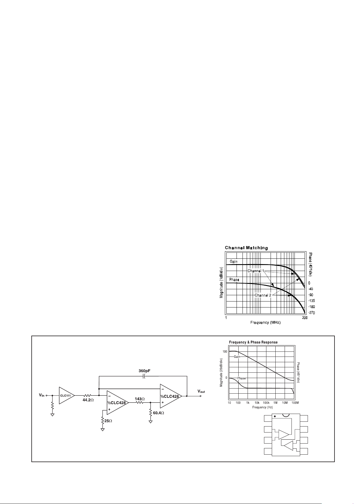
Five Decade Integrator
A composite integrator, as shown in Figure 5, uses the
CLC428 dual op amp to increase the circuits' usable
frequency range of operation. The transfer function of this
circuit is:
V
1
RC
Vdt
o
in
=
z
Eq. 4
Figure 5
A resistive divider made from the 143Ω and 60.4Ω
resistors was chosen to reduce the loop-gain and stabilize
the network. The CLC428 composite integrator provides
integration over five decades of operation. R and C set the
integrator's gain. Figure 6 shows the frequency and phase
response of the circuit in Figure 5 with R = 44.2Ω and
C = 360pF.
5 http://www.national.com
Page 6

Figure 6
Positive Peak Detector
The CLC428's dual amplifiers can be used to implement a
unity-gain peak detector circuit as shown in Figure 7.
Figure 7
The acquisition speed of this circuit is limited by the
dynamic resistance of the diode when charging C
hold
. A
plot of the of the circuit's performance is shown in Figure
8 with a 1MHz sinusoidal input.
Figure 8
A current source, built around Q1, provides the necessary
bias current for the second amplifier and prevents saturation when power is applied. The resistor, R, closes the loop
while diode D2 prevents negative saturation when Vin is
less than Vc. A MOS-type switch (not shown) can be used
to reset the capacitor's voltage.
The maximum speed of detection is limited by the delay
of the op amps and the diodes. The use of Schottky diodes
will provide faster response.
Adjustable or Bandpass Equalizer
A "boost" equalizer can be made with the CLC428 by
summing a bandpass response with the input signal, as
shown in Figure 9.
Figure 9
The overall transfer function is shown in Eq. 5.
V
V
R
KR R
s2Q
ss
Q
1
out
in
b
a
b
o
2
o
o
2
=
+
F
H
G
I
K
J
++
−
ch
ω
ω
ω
Eq. 5
To build a boost circuit, use the design equations Eq. 6 and
Eq. 7.
RC
2
Q
,2CR||R
1
Q
2
o
a
b
o
==
ωω
ch
Eq. 6,7
Select R2 and C using Eq. 6. Use reasonable values for
high frequency circuits - R2 between 10Ω and 5kΩ, C
between 10pF and 2000pF. Use Eq. 7 to determine the
parallel combination of Ra and Rb. Select Ra and Rb by
either the 10Ω to 5kΩ criteria or by other requirements
based on the impedance Vin is capable of driving. Finish
the design by determining the value of K from Eq. 8.
Peak Gain
V
V
R
KR
out
in
o
a
==−ω
ch
2
2
1
Eq. 8
Figure 10 shows an example of the response of the circuit
of Figure 9, where fo is 2.3MHz. The component values
are as follows: Ra =2.1kΩ, Rb =68.5Ω, R2 =4.22kΩ, R
=500Ω, KR =50Ω, C =120pF.
Figure 10
Q
1
http://www.national.com 6
Page 7

This page intentionally left blank.
7 http://www.national.com
Page 8

CLC428
Dual Wideband, Low-Noise, Voltage Feedback Op Amp
http://www.national.com
8
Customer Design Applications Support
National Semiconductor is committed to design excellence. For sales, literature and technical support, call the
National Semiconductor Customer Response Group at 1-800-272-9959 or fax 1-800-737-7018.
Life Support Policy
National’s products are not authorized for use as critical components in life support devices or systems without the express written approval
of the president of National Semiconductor Corporation. As used herein:
1. Life support devices or systems are devices or systems which, a) are intended for surgical implant into the body, or b) support or
sustain life, and whose failure to perform, when properly used in accordance with instructions for use provided in the labeling, can
be reasonably expected to result in a significant injury to the user.
2. Acritical component is any component of a life support device or system whose failure to perform can be reasonably expected to
cause the failure of the life support device or system, or to affect its safety or effectiveness.
National Semiconductor National Semiconductor National Semiconductor National Semiconductor
Corporation Europe Hong Kong Ltd. Japan Ltd.
1111 West Bardin Road Fax: (+49) 0-180-530 85 86 2501 Miramar Tower Tel: 81-043-299-2309
Arlington, TX 76017 E-mail: europe.support.nsc.com 1-23 Kimberley Road Fax: 81-043-299-2408
Tel: 1(800) 272-9959 Deutsch Tel: (+49) 0-180-530 85 85 Tsimshatsui, Kowloon
Fax: 1(800) 737-7018 English Tel: (+49) 0-180-532 78 32 Hong Kong
Francais Tel: (+49) 0-180-532 93 58 Tel: (852) 2737-1600
Italiano Tel: (+49) 0-180-534 16 80 Fax: (852) 2736-9960
National does not assume any responsibility for use of any circuitry described, no circuit patent licenses are implied and National reserves the right at any time without notice to change said
circuitry and specifications.
 Loading...