

Page 1
Features
■
Single +5V supply
■
Input includes V
EE
■
94MHz unity-gain bandwidth
■
-74/-94dBc HD2/HD3
■
60mA output current
■
7.5ns rise/fall time (1Vpp)
■
46ns settling time to 0.1%
Applications
■
Video ADC driver
■
Desktop multimedia
■
Single supply cable driver
■
Instrumentation
■
Video cards
■
Wireless IF amplifiers
■
Telecommunications
General Description
The Comlinear CLC427 is a dual wideband voltage-feedback
operational amplifier that is uniquely designed to provide high
performance from a single power supply. This CLC427 provides
near rail-to-rail operation and the common-mode input range
includes the negative rail. Each of the CLC427’s amplifiers offers
plenty of headroom for single-supply applications as evidenced
by its 4.3Vppoutput voltage from a single 5V supply.
Fabricated with a high-speed complementary bipolar process,
the CLC427 delivers a wide 94MHz unity-gain bandwidth, 7.5ns
rise/fall time and 150V/µs slew rate. For single supply applications
such as video distribution or desktop multimedia, the CLC427
offers low 0.35%, 0.55° differential gain and phase errors.
Each of the CLC427’s amplifiers provides high signal fidelity
with -74/-94dBc 2nd/3rd harmonics (1Vpp, 1MHz, RL=150Ω).
Combining this high fidelity performance with CLC427’s quick
46ns settling time to 0.1% makes it an excellent choice for ADC
buffering.
With its traditional voltage-feedback architecture and high-speed
performance, the CLC427 is the perfect choice for composite
signal conditioning circuit functions such as active filters,
integrators, differentiators, simple gain blocks and buffering.
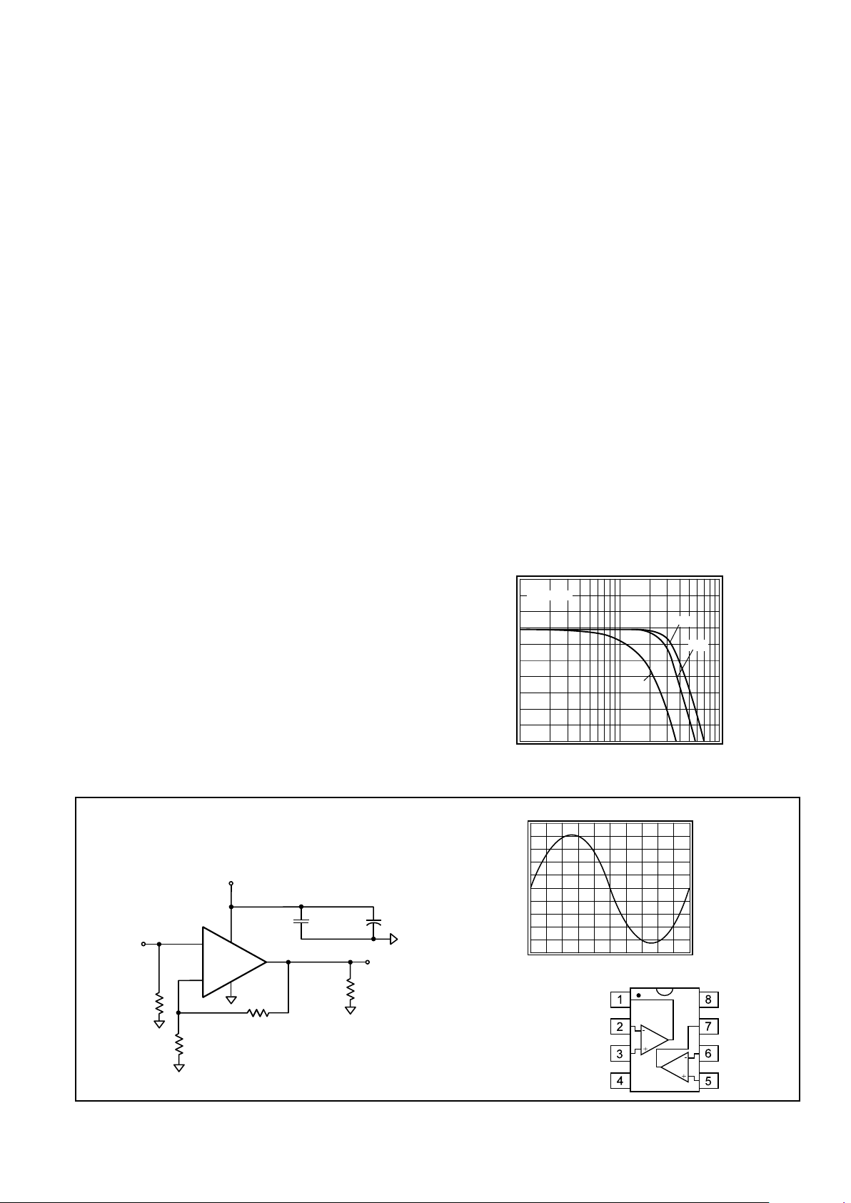
V
in
50Ω
250Ω
+
-
250Ω
0.1µF
6.8µF
150Ω
NOTE: Vin = 0.15V to 2.3V
1/2
CLC427
V
o
+5V
+
Typical Application
Single +5V Supply operation
Comlinear CLC427
Dual Voltage Feedback Amplifier
for Single Supply Operation
Frequency Response vs. V
out
Magnitude (1dB/div)
Frequency (MHz)
1
10
100
1V
pp
2V
pp
4V
pp
Av = +2V/V
V
o1
V
inv1
V
non-inv1
V
EE
V
o2
V
inv2
V
non-inv2
V
CC
Pinout
DIP & SOIC
Single Supply Response
Output Voltage (V)
Time (100ns/div)
VEE 0
1
2
3
4
V
CC
5
August 1996
Comlinear CLC427
Dual Voltage Feedback Amplifier for Single Supply Operation
N
© 1996 National Semiconductor Corporation http://www.national.com
Printed in the U.S.A.
Page 2
http://www.national.com 2
PARAMETERS CONDITIONS TYP MIN/MAX RATINGS UNITS NOTES
CLC427AJ 25° 25° 0° to +70° -40° to +85°
FREQUENCY DOMAIN RESPONSE
-3dB bandwidth V
o
< 1.0V
pp
48 32 28 27 MHz B
-3dB bandwidth V
o
< 3.0V
pp
26 16 14 11 MHz
-3dB bandwidth A
V
= +1V/V Vo< 1.0V
pp
94 MHz
rolloff <10MHz 0.1 0.5 0.7 0.8 dB B
peaking DC to 200MHz 0 0.5 0.7 0.8 dB B
linear phase deviation <15MHz 0.3 0.6 0.8 0.9 deg
differential gain NTSC, R
L
=150Ω 0.35 0.7 – – % 2
differential phase NTSC, R
L
=150Ω 0.55 2 – – deg 2
TIME DOMAIN RESPONSE
rise and fall time 1V step 7.5 13 14 16 ns
settling time to 0.1% 1V step 46 70 – – ns
overshoot 1V step 5 13 – – %
slew rate A
V
= +2 2V step 150 90 83 65 V/µs
DISTORTION AND NOISE RESPONSE
2
nd
harmonic distortion 1Vpp, 1MHz 74 – – – -dBc
1V
pp
, 5MHz 62 55 52 52 -dBc B
3
rd
harmonic distortion 1Vpp, 1MHz 94 – – – -dBc
1V
pp
, 5MHz 75 65 63 62 -dBc B
equivalent input noise
voltage >1MHz 10 12.5 13.6 14 nV/√Hz
current >1MHz 4 5 5.5 5.7 pA/√Hz
crosstalk, input referred 10MHz 65 59 59 59 -dB
STATIC DC PERFORMANCE
input offset voltage 2 7 8 10 mV A
average drift 4 – 22 35 µV/˚C
input bias current 17 30 36 45 µAA
average drift 80 – 145 175 nA/˚C
input offset current 0.2 5 6 7.5 µA
average drift 10 – 22 27 nA/˚C
power supply rejection ratio DC 82 65 64 60 dB B
common-mode rejection ratio DC 82 55 53 50 dB
supply current (per amplifier) no load 7 8.5 8.5 8.5 mA A
MISCELLANEOUS PERFORMANCE
input capacitance 1 2 2 2 pF
input resistance 700 500 450 360 kΩ
output impedance @DC 0.07 0.15 0.24 0.7 Ω
input voltage range, high 3.7 3.45 3.25 3.15 V
input voltage range, low 0 0 0 0 V
output voltage range, high R
L
= 150Ω 4.5 4.35 4.3 4.2 V
output voltage range, low R
L
= 150Ω 0.35 0.5 0.5 0.55 V
output voltage range, high no load 4.8 4.6 4.55 4.45 V
output voltage range, low no load 0.45 0.65 0.7 0.75 V
output current source 60 50 40 34 mA
output current sink 36 20 16 10 mA
supply voltage, maximum 7 7 7 V 1
supply voltage, minimum 4 4 4 V 1
transistor count = 124
Min/max ratings are based on product characterization and simulation. Individual parameters are tested as noted. Outgoing quality levels are
determined from tested parameters.
Electrical Characteristics
(Vs= +5V1, Vcm= +2.5V, Av= +2, Rf= 250
W,
RL= 150Wto GND; unless specified)
Absolute Maximum Ratings
supply voltage (Vs)
+7
V
I
out
is short circuit protected to ground
common-mode input voltage
VEEto V
CC
maximum junction temperature +175˚C
storage temperature range -65˚C to +150˚C
lead temperature (soldering 10 sec) +260˚C
differential input voltage ±2V
ESD tolerance (Note 3) 2000V
Notes
A)J-level: spec is 100% tested at 25°C, sample tested at 85°C.
B)J-level: spec is sample tested at 25°C.
1) V
s
= VCC– VEE.
2) Tested with R
L
tied to +2.5V.
3) Human body model, 1.5kΩ in series with 100pF.
Page 3
3 http://www.national.com
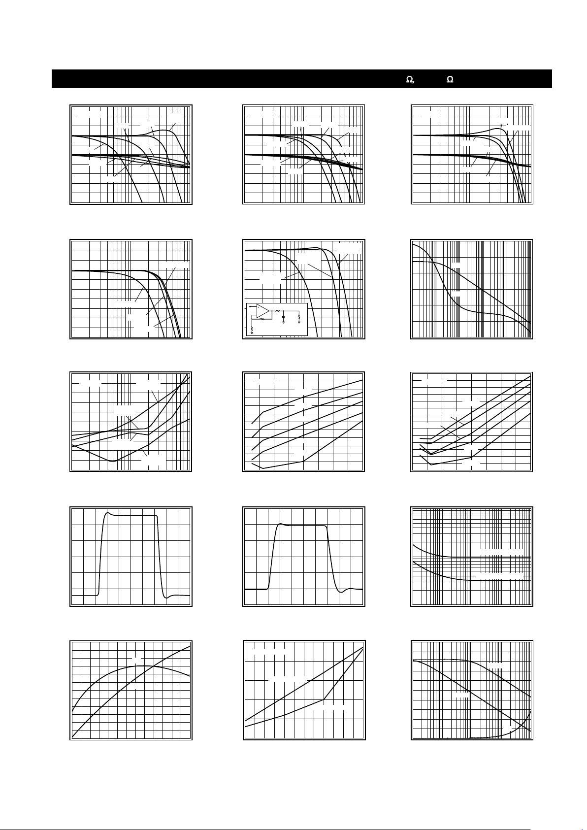
Typical Performance Characteristics
(Vs= +5V1, Vcm= +2.5V , Av= +2, Rf=250
W,
RL= 150Wto GND; unless specified)
Non-Inverting Frequency Response
Magnitude (1dB/div)
Frequency (MHz)
1
10
100
Av = 1
Rf = 0
Phase (deg)
-225
-180
-135
-90
-45
0
Av = 2
Av = 4
Av = 10
Av = 10
Av = 4
Av = 2
Av = 1
Vo = 0.25V
pp
Inverting Frequency Response
Magnitude (1dB/div)
Frequency (MHz)
1
10
100
Av = -1
Phase (deg)
-45
0
45
90
135
180
Av = -2
Av = -5
Av = -10
Av = -10
Av = -5
Av = -2
Av = -1
Vo = 0.25V
pp
Frequency Response vs. R
L
Magnitude (1dB/div)
Frequency (MHz)
0
10
100
RL = 1kΩ
Phase (deg)
-225
-180
-135
-90
-45
0
45
90
135
180
225
RL = 150Ω
RL = 75Ω
RL = 75Ω
RL = 150Ω
RL = 1kΩ
Vo = 0.25V
pp
Frequency Response vs. V
out
Magnitude (1dB/div)
Frequency (MHz)
1
10
100
Vo = 4V
pp
Vo = 2V
pp
Vo = 0.25V
pp
Vo = 1V
pp
Frequency Response vs. C
L
Magnitude (1dB/div)
Frequency (MHz)
1
10
100
CL = 10pF
R
s
= 249Ω
CL = 1000pF
R
s
= 22Ω
CL = 100pF
R
s
= 54.9Ω
1k
250Ω
250Ω
R
s
C
L
Open Loop Gain & Phase
Open Loop Gain (dB)
Frequency (MHz)
0.001 0.01 0.1 1 10
100
Phase (deg)
-120
Gain
-20
-100
0
-80
20
-60
40
-40
60
-20
80
0
100
Phase
Harmonic Distortion vs. Frequency
Distortion (dBc)
Frequency (MHz)
0.1 1
10
2nd
RL = 150Ω
-100
-90
-80
-70
-60
-50
3rd
RL = 150Ω
3rd
RL = 1kΩ
2nd
RL = 1kΩ
Vo = 1V
pp
2nd Harmonic Distortion vs. V
out
Distortion (dBc)
Output Amplitude (Vpp)
0123
4
R
L
= 150Ω
-80
-70
-60
-50
-40
-30
10MHz
5MHz
2MHz
1MHz
0.1MHz
-90
3rd Harmonic Distortion vs. V
out
Distortion (dBc)
Output Amplitude (Vpp)
0123
4
R
L
= 150Ω
-80
-70
-60
-50
-40
-30
10MHz
5MHz
2MHz
1MHz
0.1MHz
-90
-100
Small Signal Pulse Response
Output Voltage (0.05V/div)
Time (20ns/div)
Large Signal Pulse Response
Output Voltage (0.5V/div)
Time (20ns/div)
Equivalent Input Noise
Voltage Noise (nV/Hz)
Frequency (MHz)
0.001
0.1
10
Current Noise (pA/Hz)
1
Voltage = 9.5nV/√Hz
1
10
10
100
100
10.01
Current = 3.2pA/√Hz
IB, VIO, vs. Temperature
V
IO
(mV)
Temperature (°C)
-40
-200 204060
I
B
(µA)
-22
I
B
0.5
-20
0.7
-18
0.9
-16
1.1
-14
1.3
-12
1.5
-10
1.7
V
IO
80
Differential Gain and Phase (3.58MHz)
Gain (%)
Number of 150Ω Loads
1234
Phase (deg)
0
0
0.5
0.5
1
1
1.5
1.5
2
2
2.5
2.5
Phase Neg Sync
Gain Neg Sync
RL tied to +2.5V
PSRR, CMRR & Linear R
out
vs. Frequency
PSRR, CMRR (dB)
Frequency (MHz)
0.001 0.01 0.1 1
Output Resistance (Ω)
0
0
5
20
10
40
15
60
20
80
25
100
10
PSRR
R
out
CMRR
Page 4

http://www.national.com 4
CLC427 OPERATIONS
Description
The CLC427 contains two single supply voltage-feedback amplifiers. The CLC427 is a dual version of the
CLC423 with the following features:
• Operates from a single +5V supply
• Maintains near rail-to-rail performance
• Includes the negative rail (0V) in the Common
Mode Input Range (CMIR)
• Offers low -74/-94dBc 2nd and 3rd harmonic
distortion
• Provides BW > 20MHz and 1MHz distortion
< -50dBc at Vo = 4V
pp
Single Supply Operation (VCC= +5V, VEE= GND)
The CLC427 is designed to operate from 0 and 5V
supplies. The specifications given in the
Electrical
Characteristics
table are measured with a common
mode voltage (Vcm) of 2.5V. Vcmis the voltage around
which the inputs are applied and the output voltages are
specified.
Operating from a single +5V supply, the CMIR of the
CLC427 is typically 0V to +3.7V. The typical output range
with RL= 150Ω is +0.35V to +4.5V.
For simple single supply operation, it is recommended
that input signal levels remain above ground. For input
signals that drop below ground, AC coupling and level
shifting the signal are possible remedies. For input
signals that remain above ground, no adjustments need
to be made. The non-inverting and inverting
configurations for both input conditions are illustrated in
the following 2 sections.
Standard Single Supply Operation
Figures 1 and 2 show the recommended non-inverting
and inverting configurations for purely positive input
signals.
Figure 1: Non-inverting Configuration
Figure 2: Inverting Configuration
Single Supply Operation for Inputs that go below 0V
Figures 3 and 4 show possible non-inverting and inverting configurations for input signals that go below ground.
The input is AC coupled to prevent the need for level
shifting the input signal at the source. The resistive voltage divider biases the non-inverting input to VCC÷2 =
2.5V.
Figure 3: AC Coupled Non-inverting Configuration
Figure 4: AC Coupled Inverting Configuration
+
-
1/2
CLC427
R
f
0.1µF
6.8µF
V
o
V
in
+5V
R
g
R
t
3(5)
2(6)
4
8
1(7)
V
V
1
R
R
o
in
f
g
=+
+
+
-
1/2
CLC427
R
f
0.1µF
6.8µF
V
o
V
in
+5V
R
b
3(5)
2(6)
4
8
1(7)
R
g
R
t
V
VRR
o
in
f
g
=−
Select R to yield
desired R R ||R
t
in
tg
=
+
+
-
1/2
CLC427
R
f
0.1µF
6.8µF
V
o
V
in
+5V
R
g
R
3(5)
2(6)
4
8
1(7)
C
C
c
R
+
VV1
R
R
2.5
o
in
f
g
=+
+
low frequency cutoff
1
2RC
,where: R
R
2
in
c
in
==
π
2.5V
RC RC
gc
>>
+
-
1/2
CLC427
R
f
0.1µF
6.8µF
V
o
V
in
+5V
R
3(5)
2(6)
4
8
1(7)
C
c
R
+
VV
R
R
2.5
o
in
f
g
=−
+
low frequency cutoff
1
2RC
gc
=
π
2.5V
R
g
R >> R
source
Page 5

5 http://www.national.com
Load Termination
Since the CLC427 design has been optimized for Single
Supply Operation, it is more capable of sourcing rather
than sinking current. For optimum performance, the load
should be tied to VEE. When the load is tied to VEE, the
output always sources current.
Output Overdrive Recovery
When the output range of an amplifier is exceeded, time
is required for the amplifier to recover from this over
driven condition. Figure 5 illustrates the overload
recovery of the CLC427 when the output is overdriven.
An input was applied in an attempt to drive the
output to twice the supply rails, VCC- V
EE
= 10V, but
the output limits. An inverting gain topology was used,
see Figure 2. As indicated, the CLC427 recovers within
25ns on the rising edge and within 10ns on the falling
edge.
Figure 5: Overdrive Recovery
Channel Matching
Channel matching and crosstalk rejection are largely
dependent on board layout. The layout of Comlinear’s
dual amplifier evaluation boards are designed to produce
optimum channel matching and isolation. Channel
matching for the CLC427 is shown in Figure 6.
Figure 6: Channel Matching
The CLC427’s channel-to-channel isolation is better than
-70dB for video frequencies of 4MHz. Input referred
crosstalk vs frequency is illustrated in Figure 7. Pulsed
crosstalk is shown in Figure 8.
Figure 7: Input Referred Crosstalk vs. Frequency
Figure 8: Pulsed crosstalk
Driving Cables and Capacitive Loads
When driving cables, double termination is used to
prevent reflections. For capacitive load applications, a
small series resistor at the output of the CLC427 will
improve stability. The
Frequency Response vs.
Capacitive Load
plot, in the typical performance
section, gives the recommended series resistance value
for optimum flatness at various capacitive loads.
Power Dissipation
The power dissipation of an amplifier can be described in
two conditions:
• Quiescent Power Dissipation PQ(No Load Condition)
• Total Power Dissipation PT(with Load Condition)
The following steps can be taken to determine the power
consumption for each CLC427 amplifier:
1. Determine the quiescent power
PQ= ICC(VCC– VEE)
2. Determine the RMS power at the output stage
PO= (VCC– V
load
) (I
load
)
3. Determine the total RMS power
PT= PQ+ P
O
Add the total RMS powers for both channels to determine
the power dissipated by the dual.
Input Voltage (4V/div)
Time (50ns/div)
Output Voltage (2V/div)
Input
Output
Magnitude (0.5dB/div)
Frequency (MHz)
Channel A
Channel B
V
out
= 0.25V
pp
110
Crosstalk (dB)
Frequency (MHz)
1
10
100
-100
-90
-80
-70
-60
-50
-40
Output Channel A (1V/div)
Time (50ns/div)
Output Channel B (20mV/div)
Channel A
Channel B
Page 6

http://www.national.com 6
The maximum power that the package can dissipate at a
given temperature is illustrated in the
Power Derating
curves in the
Typical Performance
section. The power
derating curve for any package can be derived by
utilizing the following equation:
where: T
amb
= Ambient temperature (°C)
θJA= Thermal resistance, from junction to
ambient, for a given package (°C/W)
Layout Considerations
A proper printed circuit layout is essential for achieving
high frequency performance. Comlinear provides evaluation boards for the CLC427 (730038 - DIP, 730036SOIC) and suggests their use as a guide for high
frequency layout and as an aid for device testing and
characterization.
General layout and supply bypassing play major roles in
high frequency performance. Follow the steps below as
a basis for high frequency layout:
1. Include 6.8µF tantalum and 0.1µF ceramic
capacitors on both supplies.
2. Place the 6.8µF capacitors within 0.75 inches
of the power pins.
3. Place the 0.1µF capacitors within 0.1 inches
of the power pins.
4. Remove the ground plane under and around
the part, especially near the input and output
pins to reduce parasitic capacitance.
5. Minimize all trace lengths to reduce series
inductances.
Additional information is included in the evaluation board
literature.
T ypical Application Circuit
The typical application shown on the front page illustrates
the near rail-to-rail performance of the CLC427.
Multiple Feedback Bandpass Filter
Figure 9 illustrates a bandpass filter and design
equations. The circuit operates from a single supply of
+5V . The voltage divider biases the non-inverting input to
2.5V. The input is AC coupled to prevent the need for
level shifting the input signal at the source. Use the
design equations to determine R1and R2based on the
desired Q and center frequency.
This example illustrates a bandpass filter with Q = 4 and
center frequency fc= 1MHz. Figure 10 indicates the
filter response.
Figure 9: Bandpass Filter Topology
Figure 10: Bandpass Response
Distribution Amplifier
Figure 1 1 illustrates a distribution amplifier. The topology
utilizes the dual amplifier package. The input is
AC coupled and the non-inverting terminals of both
amplifiers are biased at 2.5V.
Figure 11: Distribution Amplifier
175 T
amb
JA
°−
()
θ
Applications Circuits
Magnitude (dB)
Frequency (MHz)
40
30
20
-10
1
10
10
0
30.6dB
940kHz
+
-
1/2
CLC427
R2
3.16kΩ
0.1µF
6.8µF
V
o
V
in
+5V
5.1kΩ
3(5)
2(6)
4
8
1(7)
5.1kΩ
+
C
390pF
C
390pF
R1
50Ω
R
Q
fc
f resonant frequency
R
R
4Q
A 2Q A mid bandgain
2
r
r
1
2
2
2
==
===−
π
+
-
1/2
CLC427
R
f
0.1µF
6.8µF
V
o
1
V
in
+5V
R
g
R
3(5)
2(6)
8
1(7)
C
C
C
R
+
R
o
R
o
R
o
Z
o
+
-
1/2
CLC427
R
f
V
o
2
R
g
3(5)
2(6)
4
1(7)
C
R
o
R
o
Z
o
Page 7

7 http://www.national.com
DC Coupled Single-to-Differential Converter
ADC coupled single-to-differential converter is illustrated in
Figure 12.
Figure 12: Single-to-Differential Converter
+
-
1/2
CLC427
0.1µF
6.8µF
V
H
(Av = +1V/V)
V
in
+5V
250Ω
3(5)
2(6)
8
1(7)
+
R
t
+
-
1/2
CLC427
250Ω
V
L
(Av = -1V/V)
3(5)
2(6)
4
1(7)
3kΩ
2kΩ
V
o
Vo = VH – V
L
Vo = 2V
in
Ordering Information
Model Temperature Range Description
CLC427AJP -40˚C to +85˚C 8-pin PDIP
CLC427AJE -40˚C to +85˚C 8-pin SOIC
Package Thermal Resistance
Package
q
JC
q
JA
Plastic (AJP) 75˚/W 90˚/W
Surface Mount (AJE) 90˚/W 115˚/W
Page 8

Comlinear CLC427, Dual Voltage Feedback
Amplifier for Single Supply Operation
http://www.national.com 8 Lit #150427-002
Customer Design Applications Support
National Semiconductor is committed to design excellence. For sales, literature and technical support, call the
National Semiconductor Customer Response Group at 1-800-272-9959 or fax 1-800-737-7018.
Life Support Policy
National’s products are not authorized for use as critical components in life support devices or systems without the express written approval
of the president of National Semiconductor Corporation. As used herein:
1. Life support devices or systems are devices or systems which, a) are intended for surgical implant into the body, or b) support or
sustain life, and whose failure to perform, when properly used in accordance with instructions for use provided in the labeling, can
be reasonably expected to result in a significant injury to the user.
2. Acritical component is any component of a life support device or system whose failure to perform can be reasonably expected to
cause the failure of the life support device or system, or to affect its safety or effectiveness.
National Semiconductor National Semiconductor National Semiconductor National Semiconductor
Corporation Europe Hong Kong Ltd. Japan Ltd.
1111 West Bardin Road Fax: (+49) 0-180-530 85 86 13th Floor, Straight Block Tel: 81-043-299-2309
Arlington, TX 76017 E-mail: europe.support.nsc.com Ocean Centre, 5 Canton Road Fax: 81-043-299-2408
Tel: 1(800) 272-9959 Deutsch Tel: (+49) 0-180-530 85 85 Tsimshatsui, Kowloon
Fax: 1(800) 737-7018 English Tel: (+49) 0-180-532 78 32 Hong Kong
Francais Tel: (+49) 0-180-532 93 58 Tel: (852) 2737-1600
Italiano Tel: (+49) 0-180-534 16 80 Fax: (852) 2736-9960
National does not assume any responsibility for use of any circuitry described, no circuit patent licenses are implied and National reserves the right at any time without notice to change said
circuitry and specifications.
N
 Loading...