

Page 1
N
CLC426
Wideband, Low-Noise, Voltage Feedback Op Amp
General Description
The CLC426 combines an enhanced voltage-feedback architecture
with an advanced complementary bipolar process to provide a
high-speed op amp with very low noise (1.6nV/√Hz & 2.0pA/√Hz) and
distortion (-62/-68dBc 2nd/3rd harmonics at 1Vpp and 10MHz).
Providing a wide 230MHz gain-bandwidth product, a fast 400V/µs
slew rate and very quick 16ns settling time to 0.05% , the CLC426 is
the ideal choice for high speed applications requiring a very widedynamic range such as an input buffer for high-resolution analog-todigital converters.
The CLC426 is internally compensated for gains ≥ 2V/V and can
easily be externally compensated for unity-gain stability in applications
such as wideband low-noise integrators. The CLC426 is also equipped
with external supply current adjustment which allows the user to
optimize power, bandwidth, noise and distortion performance for each
application.
The CLC426's combination of speed, low noise and distortion and low
dc errors will allow high-speed signal conditioning applications to
achieve the highest signal-to-noise performance. To reduce design
times and assist board layout, the CLC426 is supported by an
evaluation board and SPICE simulation model available from National.
For even higher gain-bandwidth voltage-feedback op amps see the
1.9GHz CLC425 (Av ≥ 10V/V) or the 5.0GHz CLC422 (Av ≥ 30V/V).
June 1999
CLC426
Wideband, Low-Noise, Voltage Feedback Op Amp
Features
■ Wide gain-bandwidth product: 230MHz
■ Ultra-low input voltage noise: 1.6nV/√Hz
■ Very low harmonic distortion: -62/-68dBc
■ Fast slew rate: 400V/µs
■ Adjustable supply current
■ Dual ±2.5 to ±5V or single 5 to 12V supplies
■ Externally compensatable
Applications
■ Active filters & integrators
■ Ultrasound
■ Low-power portable video
■ ADC/DAC buffer
■ Wide dynamic range amp
■ Differential amps
■ Pulse/RF amp
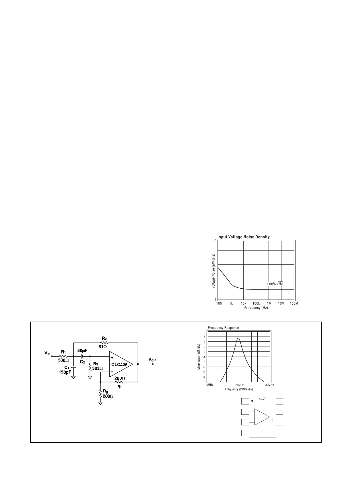
Wide Dynamic Range
Sallen-Key Band Pass Filter
2nd-Order
(20MHz, Q=10, G=2)
1
2
3
4
NC
V
inv
V
non-inv
-V
cc
R
p
(optional)
+V
cc
V
out
Ext. Comp.
(optional)
8
7
6
5
-
+
Pinout
DIP & SOIC
Typical Application
1999 National Semiconductor Corporation http://www.national.com
Printed in the U.S.A.
Page 2
CLC426 Electrical Characteristics CLC426 Electrical Characteristics
CLC426 Electrical Characteristics CLC426 Electrical Characteristics
CLC426 Electrical Characteristics
(V(V
(V(V
(V
CCCC
CCCC
CC
= =
= =
=
±±
±±
±
5V; A5V; A
5V; A5V; A
5V; A
VV
VV
V
= +2V/V; R= +2V/V; R
= +2V/V; R= +2V/V; R
= +2V/V; R
ff
ff
f
=100=100
=100=100
=100
ΩΩ
ΩΩ
Ω
; R; R
; R; R
; R
LL
LL
L
= 100= 100
= 100= 100
= 100
ΩΩ
ΩΩ
Ω
; ;
; ;
;
unless notedunless noted
unless notedunless noted
unless noted
))
))
)
A) J-level: spec is 100% tested at +25°C.
1) Minimum stable gain with out external compensation is +2 or
-1V/V, the CLC426 is unity-gain stable with external
compensation.
2) Output is short circuit protected to ground, however maximum
reliability is obtained if output current does not exceed 160mA.
3) See text for compensation techniques.
http://www.national.com 2
supply voltage ±7V
short circuit current (note 2)
common-mode input voltage ±V
cc
differential input voltage ±10V
maximum junction temperature +150°C
storage temperature -65°C to+150°C
lead temperature (soldering 10 sec) +300°C
ESD rating 2000V
Absolute Maximum Ratings
Notes
PARAMETERSPARAMETERS
PARAMETERSPARAMETERS
PARAMETERS
CONDITIONSCONDITIONS
CONDITIONSCONDITIONS
CONDITIONS
TYP TYP
TYP TYP
TYP
MIN/MAX RATINGSMIN/MAX RATINGS
MIN/MAX RATINGSMIN/MAX RATINGS
MIN/MAX RATINGS
UNITS UNITS
UNITS UNITS
UNITS
NOTESNOTES
NOTESNOTES
NOTES
Ambient Temperature CLC426 +25°C +25°C 0 to +70°C -40 to +85°C
FREQUENCY DOMAIN RESPONSE
gain bandwidth product V
out
< 0.5V
pp
230 170 120 100 MHz
-3dB bandwidth, A
v
=+2 V
out
< 0.5V
pp
130 90 70 55 MHz 1
V
out
< 5.0V
pp
50 25 22 20 MHz
gain flatness V
out
< 0.5V
pp
peaking DC to 200MHz 0.6 1.5 2.2 2.5 dB
rolloff DC to 30MHz 0.0 0.6 1.0 1.0 dB
linear phase deviation DC to 30MHz 0.2 1.0 1.5 1.5 °
TIME DOMAIN RESPONSE
rise and fall time 1V step 2.3 3.5 5.0 6.5 ns
settling time 2V step to 0.05% 16 20 2 4 2 4 n s
overshoot 1V step 5 1 5 15 18 %
slew rate 5V step 400 300 275 2 50 V/µs
DISTORTION AND NOISE RESPONSE
2
nd
harmonic distortion 1Vpp,10MHz - 62 - 52 - 47 - 45 dBc
3rd harmonic distortion 1Vpp,10MHz - 68 - 58 - 54 - 54 dBc
equivalent input noise op amp only
voltage 1MHz to 100MHz 1.6 2.0 2.3 2.6 nV/√Hz
current 1MHz to 100MHz 2. 0 3.0 3.6 4.6 pA/ √Hz
STATIC DC PERFORMANCE
open-loop gain DC 64 60 54 54 dB
input offset voltage 1.0 2.0 2.8 2.8 mV A
average drift 3 --- 1 0 10 µV/°C
input bias current 5 25 4 0 65 µAA
average drift 90 --- 60 0 70 0 nA/°C
input offset current 0.3 3 5 5 µAA
average drift 5 --- 2 5 50 nA/°C
power-supply rejection ratio DC 73 6 5 60 60 dB
common-mode rejection ratio DC 70 6 2 57 5 7 d B
supply current pin #8 open, R
L
= ∞ 11 12 13 15 mA A
MISCELLANEOUS PERFORMANCE
input resistance common-mode 500 250 125 125 kΩ
differential-mode 750 200 50 25 kΩ
input capacitance common-mode 2.0 3.0 3.0 3.0 pF
differential-mode 2.0 3.0 3.0 3.0 pF
output resistance closed loop 0.07 0.1 0.2 0.2 Ω
output voltage range R
L
= ∞ ± 3.8 ± 3.5 ± 3.3 ± 3.3 V
R
L
=100Ω ± 3.5 ± 3.2 ± 2.6 ±1.3 V
input voltage range common mode ± 3.7 ± 3. 5 ± 3 .3 ± 3.3 V
output current ± 70 ± 50 ± 4 0 + 35, -20 mA
Min/max ratings are based on product characterization and simulation. Individual parameters are tested as noted. Outgoing quality levels are
determined from tested parameters.
Model Temperature Range Description
CLC426AJP -40°C to +85°C 8-pin PDIP
CLC426AJE -40°C to +85°C 8-pin SOIC
CLC426A8B -55°C to +125°C 8-pin CerDIP, MIL-STD-883
Ordering Information
Package
θθ
θθ
θ
JC
θθ
θθ
θ
JA
Plastic (AJP) 70°C/W 125°C/W
Surface Mount (AJE) 60°C/W 140°C/W
CerDIP 40°C/W 130°C/W
Package Thermal Resistance
Transistor Count 52
Reliability Information
Page 3
3 http://www.national.com
Page 4

Introduction
The CLC426 is a wide bandwidth voltage-feedback operational amplifier that is optimized for applications requiring
wide dynamic range. The CLC426 features adjustable
supply current and external compensation for the added
flexibility of tuning its performance for demanding applications. The Typical Performance section illustrates many
of the performance trade-offs. Although designed to operate from ±5Volt power supplies, the CLC426 is equally
impressive operating from a single +5V supply. The
following discussion will enable the proper selection of
external components for optimum device performance in
a variety of applications.
External Compensation
The CLC426 is stable for noise gains ≥2V/V. For unity-gain
operation, the CLC426 requires an external compensation
capacitor (from pin 5 to ground). The plot located in the
Typical Performance section labeled "Frequency Response vs Compensation Cap." illustrates the CLC426's
typical AC response for different values of compensation
capacitor. From the plot it is seen that a value of 15pF
produces the optimal response of the CLC426 at unity
gain. The plot labeled "Open-Loop Gain vs. Compensation
Cap." illustrates the CLC426's open-loop behavior for
various values of compensation capacitor. This plot also
illustrates one technique of bandlimiting the device by
reducing the open-loop gain resulting in lower closed-loop
bandwidth. Fig. 1 shows the effect of external compensation on the CLC426's pulse response.
Application Discussion
Fig. 1
http://www.national.com 4
Page 5

Supply Current Adjustment
The CLC426's supply current can be externally adjusted
downward from its nominal value to less than 2mA by
adding an optional resistor (Rp) between pin 8 and the
negative supply as shown in fig 2. The plot labeled "OpenLoop Gain vs. Supply Current" illustrates the influence
that supply current has over the CLC426's open-loop
response. From the plot it is seen that the CLC426 can be
compensated for unity-gain stability by simply lowering
its supply current. Therefore lowering the CLC426's supply current effectively reduces its open-loop gain to the
point that there is adequate phase margin at unity gain
crossover. The plot labeled "Supply Current vs. Rp"
provides the means for selecting the value of Rp that
produces the desired supply current. The curve in the plot
represents nominal processing but a ±12% deviation over
process can be expected. The two plots labeled "Voltage
Noise vs. Supply Current" and "Current Noise vs. Supply
Current" illustrate the CLC426 supply current's effect over
its input-referred noise characteristics.
Driving Capacitive Loads
The CLC426 is designed to drive capacitive loads with the
addition of a small series resistor placed between the
output and the load as seen in fig. 3. Two plots located in
the Typical Performance section illustrate this technique
for both frequency domain and time domain applications.
The plot labeled "Frequency Response vs. Capacitive
Load" shows the CLC426's resulting AC response to
various capacitive loads. The values of Rs in this plot
were chosen to maximize the CLC426's AC response
(limited to ≤1dB peaking).
The second plot labeled "Settling Time vs. Capacitive
Load" provides the means for the selection of the value of
Rs which minimizes the CLC426's settling time. As seen
from the plot, for a given capacitive load Rs is chosen from
the curve labeled "Rs". The resulting settling time to
0.05% can then be estimated from the curve labeled "T
s
to 0.05%". The plot of fig. 4 shows the CLC426's pulse
response for various capacitive loads where Rs has been
chosen from the plot labeled "Settling Time vs. Capaci-
tive Load".
Faster Settling
The circuit of fig. 5 shows an alternative method for driving
capacitive loads that results in quicker settling times. The
small series-resistor, Rs, is used to decouple the CLC426's
open-loop output resistance, R
out
, from the load capaci-
tance. The small feedback-capacitance, Cf, is used to
provide a high-frequency bypass between the output and
inverting input. The phase lead introduced by Cf compensates for the phase lag due to CL and therefore restores
stability. The following equations provide values of Rs and
Cf for a given load capacitance and closed-loop amplifier
gain.
Eq. 1
Eq. 2
The plot in
fig. 6 shows
the result of the two methods of capacitive load driving
mentioned above while driving a 100pF||1kΩ load.
Fig. 2
Fig. 4
Fig. 5
Fig. 3
RR
R
R
whereR
C
R
R
C
R
R
s out
f
g
out
f
g
L
out
g
=
≈
=+
;6
1
1
2
Ω
Fig. 6
5 http://www.national.com
Page 6

Single-Supply Operation
The CLC426 can be operated with single power supply as
shown in fig. 7. Both the input and output are capacitively
coupled to set the dc operating point.
DAC Output Buffer
The CLC426's quick settling, wide bandwidth and low
differential input capacitance combine to form an excellent I-to-V converter for current-output DACs in such
applications as reconstruction video. The circuit of fig. 8
implements a low-noise transimpedance amplifier commonly used to buffer high-speed current output devices.
The transimpedance gain is set by Rf. A feedback
capacitor, Cf, is needed in order to compensate for the
inductive behavior of the closed-loop frequency response
of this type of circuit. Equation 3 shows a means of
calculating the value of Cf which will provide conditions for
a maximally-flat signal frequency response with approximately 65° phase margin and 5% step-response overshoot. Notice that Ct is the sum of the DAC output
capacitance and the differential input capacitance of the
CLC426 which is located in its Electrical Characteristics
Table. Notice also that CLC426's gain-bandwidth product
(GBW) is also located in the same table. Equation 5
provides the resulting signal bandwidth.
C
C
RGBW
f
t
f
=
2
2
π
Eq. 3
CC C
toutindif
=+
Eq. 4
signalbandwidth
GBW
RC
ft
=
1
22
π
Eq. 5
Sallen-Key Active Filters
The CLC426 is well suited for Sallen-Key type of active
filters. Fig. 9 shows the 2nd order Sallen-Key band-pass
filter topology and design equations.
Fig. 9
To design the band-pass, begin by choosing values for R
f
and Rg, for example
RR
fg
==
200
Ω
. Then choose reasonable values for C1 and C2 (where C1=5C2) and then
compute R1. R2 and R3 can then be computed. For
optimum high-frequency performance it is recommended
that the resistor values fall in the range of 10Ω to 1kΩ and
the capacitors be kept above 10pF. The design can
be further improved by compensating for the delay through
the op amp. For further details on this technique, please
request Application Note OA-21 from National Semiconductor Corporation.
Printed Circuit Board Layout
Generally, a good high-frequency layout will keep power
supply and ground traces away from the inverting input
and output pins. Parasitic capacitances on these nodes
to ground will cause frequency-response peaking and
possible circuit oscillation, see OA-15 for more information.
National suggests the CLC730013 (through-hole) or the
CLC730027 (SOIC) evaluation board as a guide for highfrequency layout and as an aid in device testing and
characterization.
Fig. 7
Fig. 8
CC
G
R
R
desiredmid bandgain
R
Q
GC f
where f desiredcenter frequency
R
GR Q G G
QGG
R
GR Q G G G
Q
f
g
21
1
1
2
1
22
22
3
1
22
2
1
5
1
2
2
148 2 1
48 2
51482 1
4
=
=+ −
=
()
=
=
+−++
−+
=
+−++−
,
,
.
.
.
π
http://www.national.com 6
Page 7

This page intentionally left blank.
7 http://www.national.com
Page 8

CLC426
Wideband, Low-Noise, Voltage Feedback Op Amp
http://www.national.com
8
Customer Design Applications Support
National Semiconductor is committed to design excellence. For sales, literature and technical support, call the
National Semiconductor Customer Response Group at 1-800-272-9959 or fax 1-800-737-7018.
Life Support Policy
National’s products are not authorized for use as critical components in life support devices or systems without the express written approval
of the president of National Semiconductor Corporation. As used herein:
1. Life support devices or systems are devices or systems which, a) are intended for surgical implant into the body, or b) support or
sustain life, and whose failure to perform, when properly used in accordance with instructions for use provided in the labeling, can
be reasonably expected to result in a significant injury to the user.
2. A critical component is any component of a life support device or system whose failure to perform can be reasonably expected to
cause the failure of the life support device or system, or to affect its safety or effectiveness.
National Semiconductor National Semiconductor National Semiconductor National Semiconductor
Corporation Europe Hong Kong Ltd. Japan Ltd.
1111 West Bardin Road Fax: (+49) 0-180-530 85 86 2501 Miramar Tower Tel: 81-043-299-2309
Arlington, TX 76017 E-mail: europe.support.nsc.com 1-23 Kimberley Road Fax: 81-043-299-2408
Tel: 1(800) 272-9959 Deutsch Tel: (+49) 0-180-530 85 85 Tsimshatsui, Kowloon
Fax: 1(800) 737-7018 English Tel: (+49) 0-180-532 78 32 Hong Kong
Francais Tel: (+49) 0-180-532 93 58 Tel: (852) 2737-1600
Italiano Tel: (+49) 0-180-534 16 80 Fax: (852) 2736-9960
National does not assume any responsibility for use of any circuitry described, no circuit patent licenses are implied and National reserves the right at any time without notice to change said
circuitry and specifications.
 Loading...