

Page 1
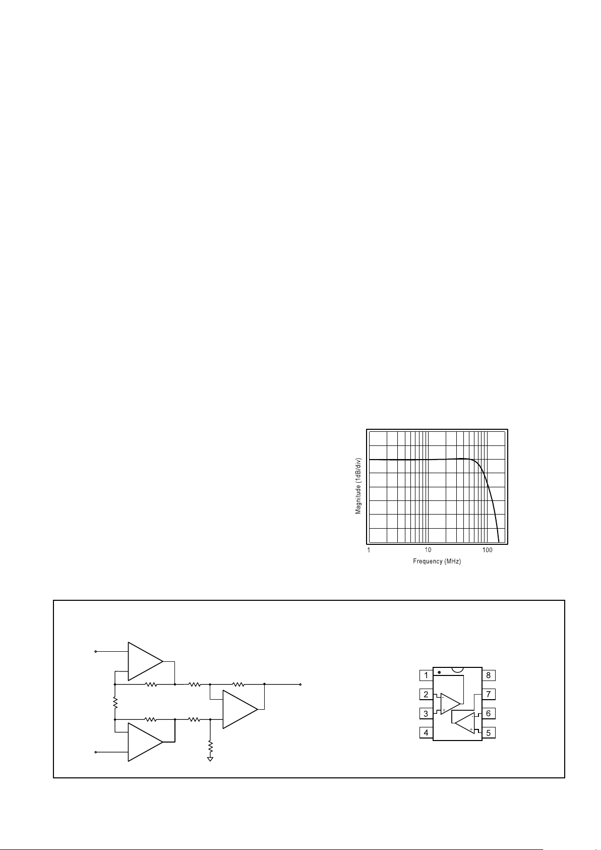
Typical Application Diagram
Instrumentation Amplifier
Pinout
DIP & SOIC
CLC416
Dual Low-Power, 120MHz Op Amp
September 1998
Features
■
0.01%, 0.03° DG, Dφ
■
Very low input bias current: 100nA
■
High input impedance: 6MΩ
■
120MHz -3dB bandwidth (Av= +2)
■
Low power
■
High output current: 60mA
■
Low-cost
Applications
■
Desktop video systems
■
Video distribution
■
Flash A/D driver
■
High-speed driver
■
High-source impedance applications
■
Professional video processing
■
High resolution monitors
General Description
The CLC416 is a dual, wideband (120MHz) op amp. The
CLC416 consumes only 39mW per channel and can source or
sink an output current of 60mA. These features make the
CLC416 a versatile, high-speed solution for demanding
applications that are sensitive to both power and cost.
Utilizing National’s proven architectures, this dual current
feedback amplifier surpasses the performance of alternative
solutions and sets new standards for low power. This powerconserving dual op amp achieves low distortion with -80dBc and
-80dBc second and third harmonics respectively. Many high
source impedance applications will benefit from the CLC416’s
6MΩ input impedance. And finally, designers will have a bipolar
part with an exceptionally low 100nA non-inverting bias current.
With 0.1dB flatness to 30MHz and low differential gain and phase
errors, the CLC416 is an ideal part for professional video
processing and distribution. The 120MHz -3dB bandwidth (Av=
+2) coupled with a 400V/µs slew rate also makes the CLC416
a perfect choice in cost-sensitive applications such as video
monitors, fax machines, copiers, and CATV systems.
Vo1
V
inv
1
V
non-inv
1
-V
CC
Vo2
V
inv
2
V
non-inv
2
+V
CC
+
-
348Ω
1/2
CLC416
R
1
348Ω
-
+
1/2
CLC416
348Ω
348Ω
V
out
= 3(V2 - V1)
348Ω
348Ω
348Ω
-
+
CLC405
V
1
V
2
Frequency Response (Av = +2V/V)
CLC416
Dual Low-Power, 120MHz Op Amp
N
© 1998 National Semiconductor Corporation http://www.national.com
Printed in the U.S.A.
Page 2
PARAMETERS CONDITIONS TYP MIN/MAX RATINGS UNITS NOTES
Ambient Temperature CLC416AJ +25˚C +25˚C 0 to 70˚C -40 to 85˚C
FREQUENCY DOMAIN RESPONSE
-3dB bandwidth V
out
< 1.0V
pp
120 65 45 45 MHz
V
out
< 5.0V
pp
52 40 36 35 MHz 1
±
0.1dB bandwidth V
out
< 1.0V
pp
30 15 MHz
gain flatness V
out
< 1.0V
pp
peaking DC to 200MHz 0.1 0.7 0.8 1.0 dB
rolloff <30MHz 0 0.3 0.6 0.6 dB
linear phase deviation <20MHz 0.3 0.6 0.7 0.7 deg
differential gain 4.43MHz, R
L
=150Ω 0.01 0.04 0.04 0.04 %
differential phase 4.43MHz, R
L
=150Ω 0.03 0.08 0.11 0.12 deg
TIME DOMAIN RESPONSE
rise and fall time 2V step 4.3 6.5 7.2 7.4 ns
settling time to 0.05% 2V step 22 30 38 41 ns
overshoot 2V step 3 12 12 12 %
slew rate A
V
= +2 2V step 400 300 260 250 V/µs
A
V
= -1 1V step 700 V/µs
DISTORTION AND NOISE RESPONSE
2
nd
harmonic distortion 2Vpp, 1MHz -80 dBc
3
rd
harmonic distortion 2Vpp, 1MHz -80 dBc
2
nd
harmonic distortion 2Vpp, 10MHz -65 -55 -50 -47 dBc
3
rd
harmonic distortion 2Vpp, 10MHz -57 -50 -45 -45 dBc
equivalent input noise
voltage >1MHz 5 6.3 6.6 6.7 nV/√Hz
inverting current >1MHz 12 15 16 17 pA/√Hz
non-inverting current >1MHz 3 3.8 4.0 4.2 pA/√Hz
crosstalk, input referred 2V
pp
, 10MHz 72 66 66 66 dB
STATIC DC PERFORMANCE
input offset voltage 1 5 7 8 mV A
average drift 30 50 50 µV/˚C
input bias current non-inverting 100 900 1600 2800 nA A
average drift 3 8 11 nA/˚C
input bias current inverting 1 5 6 8 µAA
average drift 17 40 45 nA/˚C
power supply rejection ratio DC 52 47 47 45 dB
common-mode rejection ratio DC 50 45 45 43 dB
supply current per channel R
L
= ∞ 3.9 4.5 4.6 4.9 mA A
MISCELLANEOUS PERFORMANCE
input resistance non-inverting 6 3 2.4 1 MΩ
input capacitance non-inverting 1 2 2 2 pF
common mode input range
±
2.2 ±1.8 ±1.7 ±1.5 V
output voltage range R
L
= 100Ω +3.5,-2.9 +3.1/-2.8 +2.9/-2.7 +2.4/-1.7 V
output voltage range R
L
= ∞ +4.0,-3.4 +3.9/-3.3 +3.8/-3.2 +3.7/-2.8 V
output current 60 44 38 20 mA
output resistance, closed loop 0.06 0.2 0.25 0.4 Ω
Recommended gain range +1 to +40V/V Transistor count = 110
Min/max ratings are based on product characterization and simulation. Individual parameters are tested as noted. Outgoing quality levels are
determined from tested parameters.
CLC416 Electrical Characteristics
(AV= +2, Rf= 348Ω: Vcc= + 5V, RL= 100Ω unless specified)
Absolute Maximum Ratings
supply voltage
±
7V
I
out
is short circuit protected to ground
common-mode input voltage
±
Vcc
maximum junction temperature +175˚C
storage temperature range -65˚C to +150˚C
lead temperature (soldering 10 sec) +300˚C
ESD rating (human body model) 1000V
Notes
1) At temps < 0˚C, spec is guaranteed for RL= 500Ω.
A) J-level: spec is 100% tested at +25˚C.
Ordering Information
Model Temperature Range Description
CLC416AJP -40˚C to +85˚C 8-pin PDIP
CLC416AJE -40˚C to +85˚C 8-pin SOIC
Package Thermal Resistance
Package θ
JC
θ
JA
Plastic (AJP) 80°C/W 95°C/W
Surface Mount (AJE) 95°C/W 115°C/W
http://www.national.com 2
Page 3

CLC416 Typical Performance Characteristics
(Vcc= ±5V, Av= +2, Rf= 348
ΩΩ,,
RL= 100ΩΩ; unless specified)
Frequency Response
Normalized Magnitude (1dB/div)
Frequency (MHz)
1
10
100
Vo = 0.5V
pp
Phase (deg)
-90
-180
-450
-270
-360
0
Av = 1
Rf = 1.65kΩ
Av = 2
Rf = 348Ω
Av = 4
Rf = 200Ω
Av = 10
Rf = 100Ω
Inverting Frequency Response
Normalized Magnitude (1dB/div)
Frequency (MHz)
1
10
100
Phase (deg)
-270
-360
-630
-450
-540
-180
-90
0
Av = -1
R
f
= 2kΩ
Vo = 0.5V
pp
Av = -4
Rf = 255Ω
Av = -10
Rf = 200Ω
Av = -2
Rf = 348Ω
Frequency Response vs. R
L
Magnitude (1dB/div)
Frequency (MHz)
1
10
100
Phase (deg)
-90
-180
-450
-270
-360
0
RL = 100Ω
Vo = 1V
pp
Av = +2
RL = 1kΩ
RL = 50Ω
RL = 50Ω
RL = 100Ω
RL = 1kΩ
Frequency Response vs. V
out
Magnitude (1dB/div)
Frequency (MHz)
1
10
100
1V
pp
Av = +2
0.2V
pp
2V
pp
5V
pp
Frequency Response vs. CL
Magnitude (1dB/div)
Frequency (MHz)
1
10 100
Vo = 1V
pp
Rs = 107Ω
C
L
= 10pF
Rs = 39.25Ω
C
L
= 47pF
Rs = 27.4Ω
C
L
= 100pF
Rs = 8Ω
C
L
= 1000pF
R
s
1k
348Ω
348Ω
C
L
Open Loop Transimpedance Gain, Z(s)
20 log [|V
o
/|
i
|] (dBΩ)
1k
10M
100M
Frequency (Hz)
130
110
90
70
50
30
Phase (deg)
200
160
120
80
40
0
Gain
Phase
1M
100k
10k
100Ω
-
+
CLC416
V
o
I
i
Maximum Output Voltage vs. R
L
Maximum Output Voltage (V)
Load (Ω)
0
100
200
300 400
-4
-2
0
2
4
500 600
Recommended Rs vs. Capacitive Load
R
s
(Ω)
CL (pF)
0
20
40
60
80
100
120
10
100
1000
2nd & 3rd Harmonic Distoration
Distortion Level (dBc)
Frequency (MHz)
1
10
-70
-80
-90
-60
-50
-40
Vo = 2V
pp
3rd, RL = 100Ω
2nd, RL = 100Ω
2nd, RL = 1kΩ
3rd, RL = 1kΩ
2nd Harmonic Distortion vs. P
out
Distortion (dBc)
Output Power (dBm)
-90
-85
-80
-75
-70
-65
-60
-55
-10 -5 0 5 10
1MHz
500kHz
5MHz
10MHz
50Ω
348Ω
348Ω
50Ω
P
o
3rd Harmonic Distortion vs. P
out
Distortion (dBc)
Output Power (dBm)
-100
-90
-80
-70
-60
-50
-40
-10 -5 0 5 10
1MHz
500kHz
5MHz
10MHz
50Ω
348Ω
348Ω
50Ω
P
o
Differential Gain & Phase
Gain (%)
Number of 150Ω Loads
0
1
2
4
Phase (deg)
0
0.01
0.03
0.02
0.06
0.03
0.09
0.04
0.12
0.05
0.15
0.06
0.18
0.07
0.21
0.08
0.24
0.09
0.27
0.1
0.30
Phase Negative Sync
Phase Positive Sync
Gain Positive Sync
Gain Negative
Sync
3
Small Signal Pulse Response
Output Voltage (V)
Time (5ns/div)
-0.08
-0.06
-0.04
-0.02
0
0.02
0.04
0.06
0.08
Av = +1
Av = -1
Large Signal Pulse Response
Output Voltage (V)
Time (5ns/div)
-2
-1
0
1
2
Av = +2
Av = -2
PSRR and CMRR
PSRR/CMRR (dB)
10k
100k
1M
Frequency (Hz)
10M 100M
60
50
40
30
20
10
PSRR
CMRR
3 http://www.national.com
Page 4

CLC416 Typical Performance Characteristics
(Vcc= ±5V, Av= +2, Rf= 348
ΩΩ,,
RL= 100ΩΩ; unless specified)
CLC416 OPERATION
Description
The CLC416 is a dual current feedback amplifier with
the following features:
■
Differential gain and phase errors of 0.01%
and 0.03° into a 150Ω load
■
Low, 3.9mA, supply current per amplifier
The professional video quality differential gain and
phase errors and low power capabilities of the CLC416
make this product a good choice for video applications.
Gain
The non-inverting and inverting gain equations for the
CLC416 are as follows:
Non-inverting Gain:
Inverting Gain:
Where Rfis the feedback resistor and Rgis the gain
setting resistor. Figure 1 shows the general non-inverting gain configuration including the recommended
bypass capacitors.
Figure 1: Recommended Non-Inverting Gain Circuit
Feedback Resistor Selection
The feedback resistor, Rf, determines the loop gain
and frequency response of a current feedback
amplifier. Optimum performance of the CLC416, at a
gain of +2V/V, is achieved with Rfequal to 348Ω. The
frequency response plots in the typical performance
section illustrate the recommended Rffor several
gains. Within limits, Rfcan be adjusted to optimize the
frequency response.
■
Decrease Rfto peak frequency response and
extend bandwidth
■
Increase Rfto roll off frequency response and
reduce bandwidth
As a rule of thumb, if the recommended Rfis doubled,
the bandwidth will be cut in half.
Channel Matching
Channel matching and crosstalk efficiency are largely
dependent on board layout. The layout of National’s
dual amplifier evaluation boards are designed to produce
optimum channel matching and isolation. Typical
channel matching for the CLC416 is shown in Figure 2.
Figure 2: Channel Matching
The CLC416’s channel-to-channel isolation is better
than 70dB for input frequencies of 4MHz. Input
referred crosstalk vs. frequency is illustrated in Figure 3.
Typical DC Errors vs. Temperature
Offset Voltage (mV)
Temperature (°C)
6
5
4
1
-50
0
100
3
2
I
BN
Bias Current (µA)
1
0
-1
-2
-3
50
I
BI
V
IO
Equivalent Input Noise
Noise Voltage (nV/√Hz)
Frequency (Hz)
100
10
1
1k
100
10k
100k
1M
10M
Noise Current (pA/√Hz)
100
10
1
Inverting Current = 12pA/√Hz
Voltage = 5nV/√Hz
Non-Inverting Current = 3pA/√Hz
Power Derating Curves
Power (W)
Ambient Temperature (°C)
0.8
1.0
0.6
0
0 20 40 60 80 100 120 140 160 180
0.4
0.2
AJE
AJP
1
R
R
f
g
+
−
R
R
f
g
+
-
CLC416
R
f
0.1µF
6.8µF
V
o
V
in
+V
cc
0.1µF
6.8µF
-V
cc
R
L
R
g
R
in
g
Magnitude (0.5dB/div)
Frequency (MHz)
1
10
100
Av = +2
R
L
= 100Ω
V
o
= 2V
pp
Phase (deg)
-450
-360
-270
-180
-90
0
Channel B
Channel B
Channel A
Channel A
http://www.national.com 4
Page 5

Figure 3: Input Referred Crosstalk vs. Frequency
Driving Cables and Capacitive Loads
When driving cables, double termination is used to
prevent reflections. For capacitive load applications, a
small series resistor at the output of the CLC416 will
improve stability. The
Rsvs. Capacitive Load
plot,
in the
Typical Performance
section, gives the
recommended series resistance value for optimum
flatness at various capacitive loads.
Power Dissipation
The power dissipation of an amplifier can be described
in two conditions:
■
Quiescent Power Dissipation PQ(No Load Condition)
■
Total Power Dissipation PT(with Load Condition)
The following steps can be taken to determine the
power consumption for each CLC416 amplifier:
1. Determine the quiescent power
PQ= Icc(V
CC -VEE
)
2. Determine the RMS power at the output stage
PO= (Vcc- V
load
) (I
load
), where V
load
and I
load
are the RMS voltage and current across the
external load.
3. Determine the total RMS power
PT= PQ+ P
O
Add the total RMS powers for both channels to determine the power dissipated by the dual.
The maximum power that the package can dissipate at
a given temperature is illustrated in the
Power
Derating
curves in the
Typical Performance
section.
The power derating curve for any package can be
derived by utilizing the following equation:
where: T
amb
= Ambient temperature (°C)
θJA= Thermal resistance, from junction to
ambient, for a given package (°C/W)
Layout Considerations
A proper printed circuit layout is essential for achieving
high frequency performance. National provides
evaluation boards for the CLC416 (CLC730038 - DIP,
CLC730036 - SOIC) and suggests their use as a guide
for high frequency layout and as an aid for device testing and characterization.
Supply bypassing is required for best performance.
The bypass capacitors provide a low impedance return
current path at the supply pins. They also provide high
frequency filtering on the power supply traces. Other
layout factors play a major role in high frequency
performance. The following are recommended as a
basis for high frequency layout:
1. Include 6.8µF tantalum and 0.1µF ceramic
capacitors on both supplies.
2. Place the 6.8µF capacitors within 0.75 inches
of the power pins.
3. Place the 0.1µF capacitors within 0.1 inches
of the power pins.
4. Remove the ground plane under and around
the part, especially near the input and output
pins to reduce parasitic capacitance.
5. Minimize all trace lengths to reduce series
inductances.
Additional information is included in the evaluation
board literature.
SPICE Models
SPICE models provide a means to evaluate amplifier
designs. Free SPICE models are available for
National’s monolithic amplifiers that:
■
Support Berkeley SPICE 2G and its many
derivatives
■
Reproduce typical DC, AC, Transient, and
Noise performance
■
Support room temperature simulations
The
readme
file that accompanies the diskette lists
released models, and provides a list of modeled parameters. The application note OA-18, Simulation
SPICE Models for National’s Op Amps, contains
schematics and a reproduction of the
readme
file.
Applications Circuits
Instrumentation Amplifier
An instrumentation circuit is shown on the front page
and reproduced in Figure 4. The DC CMRR can be
fine tuned by adjusting R1.
Figure 4: Instrumentation Amplifier
P
(175 Tamb)
JA
=
°−
θ
+
-
348Ω
1/2
CLC416
R
1
348Ω
-
+
1/2
CLC416
348Ω
348Ω
V
out
= 3(V2 - V1)
348Ω
348Ω
348Ω
-
+
CLC405
V
1
V
2
Crosstalk (dB)
Frequency (MHz)
-120
-100
-80
-60
-40
-20
1
100
10
5 http://www.national.com
Page 6

Differential Line Receiver
Figure 5 illustrates a Differential Line Receiver. The
circuit will convert differential signals to single-ended signals.
Figure 5: Differential Line Receiver
Bandpass Filter
Figure 6 illustrates a low-sensitivity bandpass filter and
design equations. This topology utilizes the CLC416’s
closely matched amplifiers to obtain low op-amp
sensitivity at high frequencies. The CLC405 is used as
a buffer to obtain low output impedance. The overall
circuit gain is unity. For additional gain, the CLC405
can be configured as a non-inverting amplifier.
To design the filter, choose C and then determine values
for R and R1based on the desired resonant frequency
(fr) and Q factor.
Figure 7 illustrates a bandpass filter with Q = 10 and
fr= 1MHz. The component values used are listed
below:
R1= 4.9kΩ
R = 499Ω
C = 330pF
Rf= 2kΩ
Figure 6: Bandpass Filter Topology
Figure 7: Bandpass Response
Customer Design Applications Support
National Semiconductor is committed to design excellence. For sales, literature and technical support, call the
National Semiconductor Customer Response Group at 1-800-272-9959 or fax 1-800-737-7018.
Life Support Policy
National’s products are not authorized for use as critical components in life support devices or systems without the express written approval
of the president of National Semiconductor Corporation. As used herein:
1. Life support devices or systems are devices or systems which, a) are intended for surgical implant into the body, or b) support or
sustain life, and whose failure to perform, when properly used in accordance with instructions for use provided in the labeling, can
be reasonably expected to result in a significant injury to the user.
2. Acritical component is any component of a life support device or system whose failure to perform can be reasonably expected to
cause the failure of the life support device or system, or to affect its safety or effectiveness.
National Semiconductor National Semiconductor National Semiconductor National Semiconductor
Corporation Europe Hong Kong Ltd. Japan Ltd.
1111 West Bardin Road Fax: (+49) 0-180-530 85 86 13th Floor, Straight Block Tel: 81-043-299-2309
Arlington, TX 76017 E-mail: europe.support.nsc.com Ocean Centre, 5 Canton Road Fax: 81-043-299-2408
Tel: 1(800) 272-9959 Deutsch Tel: (+49) 0-180-530 85 85 Tsimshatsui, Kowloon
Fax: 1(800) 737-7018 English Tel: (+49) 0-180-532 78 32 Hong Kong
Francais Tel: (+49) 0-180-532 93 58 Tel: (852) 2737-1600
Italiano Tel: (+49) 0-180-534 16 80 Fax: (852) 2736-9960
National does not assume any responsibility for use of any circuitry described, no circuit patent licenses are implied and National reserves the right at any time without notice to change said
circuitry and specifications.
+
-
R
1/2
CLC416
+
-
CLC405
V
o
R
R
-
+
1/2
CLC416
V
in
R
R
f
R
1
C
C
R
1
2fC
RQR
r
1
==
π
Magnitude (dB)
Frequency (MHz)
0
-10
-40
1
10
-20
-30
1.8dB
935kHz
CLC416
Dual Low-Power, 120MHz Op Amp
-
+
Vo = 2V
in
-V
in
R
R
R
R
Av = -1V/V
-
+
1/2
CLC416
1/2
CLC416
+V
in
R
R
R
o
Av = -1V/V
R
N
http://www.national.com 6
 Loading...