

Page 1
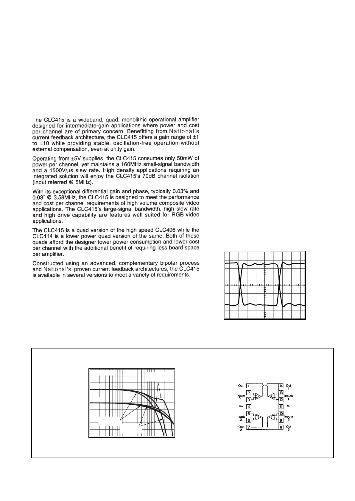
Small Signal Pulse Response
5ns/div
Output Voltage
A =+6
v
V = 2Vpp
o
+1.2
+0.8
+0.4
0
-0.4
-0.8
-1.2
A =-5
v
Features
■
160MHz small signal bandwidth
■
5mA quiescent current per amplifier
■
70dB channel isolation @ 5MHz
■
0.03%/0.03° differential gain/phase
■
12ns settling to 0.1%
■
1500V/µs slew rate
■
2.0ns rise and fall time (2Vpp)
■
70mA output current per amplifier
Applications
■
Composite video distribution amps
■
HDTV amplifiers
■
RGB-video amplifiers
■
CCD signal processing
■
Active Filters
■
Instrumentation differential amps
■
Channelized EW
General Description
CLC415
Quad,Wideband Monolithic Op Amp
N
June 1999
CLC415
Quad,Wideband Monolithic Op Amp
Non-Inverting Frequency Response
Magnitude (1dB/div)
1 Frequency (MHz) 100
Phase
0
-90
°
-180
°
-270
°
-360
°
-450
°
Vo = 2V
pp
Av = 6
Rf = 499Ω
A
v
= 2
Rf = 698Ω
A
v
= 10
Rf = 200Ω
Gain
Phase
Pinout
DIP & SOIC
© 1999 National Semiconductor Corporation http://www.national.com
Printed in the U.S.A.
CLC415AJP -40°C to +85°C 14-pin plastic DIP
CLC415AJE -40°C to +85°C 14-pin plastic SOIC
DESC SMD number: 5962-90994
Page 2
CLC415 Electrical Characteristics
(Av= +6,Vcc= ±5V, RL= 100Ω,Rf= 500Ω; unless specified)
2
Absolute Maximum Ratings Miscellaneous Ratings
http://www.national.com 2
Min/max ratings are based on product characterization and simulation. Individual parameters are tested as noted. Outgoing quality levels are
determined from tested parameters.
Pac kage Thermal Resistance
Package θ
JC
θ
JA
AJP 55°C/W 105°C/W
AJE 45°C/W 115°C/W
CERDIP 30°C/W 80°C/W
Reliability Information
Transistor count 144
Page 3

CLC415 Typical Performance Characteristics
(TA= 25°,Av= +6,VCC= ±5V ,RL= 100
ΩΩ,,
Rf= 500ΩΩ;unless specified)
Inverting Frequency Response
-180°
-270°
-360°
-450°
-540°
-630°
Phase
1 Frequency (MHz) 100
Magnitude (1dB/div)
Frequency Response for Various R s
Phase
0 20MHz/div 200MHz
V = 2Vpp
R
L
=50
=100
=100
=1k
=50
o
Magnitude (1dB/div)
L
0°
-45°
-90°
-135°
-180°
R
L
R
L
R
L
R
L
Small Signal Pulse Response
5ns/div
Output Voltage
A =+6
v
V = 2Vpp
o
+1.2
+0.8
+0.4
0
-0.4
-0.8
-1.2
A =-5
v
Short-Term Settling Time
0.20
0.15
0.10
0.05
0
-0.05
-0.10
-0.15
-0.20
Settling Error (%)
2V output step
Long-Term Settling Time
+0.20
+0.15
+0.10
+0.05
0
-0.05
-0.10
-0.15
-0.20
Settling Error
(% of output step final value)
2V output step
Time (s)
-40
-50
-60
-70
-80
Distortion (dBc)
1 2 5 10 20 50
Frequency (MHz)
2nd, R =100
Ω
L
3rd, R =100
Ω
L
3rd, R =1k
Ω
L
2nd, R =1k
L
Ω
100
Ω
L
R
-
+
2V
pp
500
Ω
2-Tone, 3rd Order Spurious Levels
-30
-40
-50
-60
-70
-80
3rd Order Spurious (dBc)
Test Tone Power (P , dBm-each tone)
-4 -2 0 2 4
-
+
50
Ω
out
P
100
Ω
500
Ω
50
Ω
40MHz
50MHz
30MHz
out
Settling Time vs. Capacitive Load
50
40
30
20
10
0
Settling Time, Ts(ns) to 0.05%
10 100 1000
Load Capacitance, C (pF)
50
40
30
20
10
0
R (ohms)
s
0.25
0.20
0.15
0.10
0.05
0
Differential Gain (%)
Number of 150 loads
1 2 3 4
Differential Phase (degrees)
.30
.25
.20
.15
.10
0
Phase Positive
sync
Equivalent Input Noise
100
Noise Voltage (nV/ Hz )
10 10 10 10 10 10 10
10
1
Frequency (Hz)
Noise Current (pA/ Hz )
2
34
6
7
8
5
Inverting Current =
11.5pA/ Hz
Voltage =3.0nV/ Hz
Gain
Phase
Gain
Phase
R
L
=1k
10 10 10 10 10 10 10 10 10 10
-9 -8 -7 -6 -5 -4 -3 -2 -1 0
R
s
PSRR, CMRR, and Closed Loop R
60
50
40
30
20
10
10 10 10 10 10
Frequency (Hz)
4
5
8
67
PSRR/CMRR (dB)
R
PSRR
Open-Loop Transimpedance Gain, Z(s)
130
120
110
100
90
80
70
60
50
40
30
10 10 10 10 10 10
Frequency (Hz)
4
53
6
7
200
180
160
140
120
100
80
60
40
20
20 log [ V /I / 1 ]
o
Ω
Phase (degrees)
o
CMRR
o
30
20
10
0
-10
-20
20log (R )
o
i
Ω
Ω
Ω
Ω
Ω
Ω
0 100
10ns/div
20MHz
10MHz
L
1k
R
s
-
+
100
Ω
500
Ω
C
L
Ω
T
s
105
95
85
75
65
55
45
35
25
15
10 10 10 10
Frequency (Hz)
5
8
67
Crosstalk Isolation (dB)
All Hostile Crosstalk Isolation
R =1k
L
Ω
R =100LΩ
Ω
Phase
Negative sync
Gain
Positive sync
Gain
Negative sync
V
out
-
+
75
Ω
75
Ω
75
Ω
V
out
Non-Inverting Current=
2.0pA/ Hz
50
20
5
2
Phase
Gain
2nd and 3rd Harmonic Distortion
Most Susceptible Channel-Channel Pulse Coupling
2V/div
20mV/div
Volts
Time (100ns/div)
10mV/div
Coupled
Signal
Driven
Signal
R =100
L
Ω
R =1k
L
Ω
8
-
+
100
V
o
I
Ω
i
Differential Gain and Phase (4.43 MHz, A =+2)
v
Non-Inverting Frequency Response
Magnitude (1dB/div)
1 Frequency (MHz) 100
Phase
0
-90
°
-180
°
-270
°
-360
°
-450
°
Vo = 2V
pp
Av = 6
Rf = 499Ω
A
v
= 2
Rf = 698Ω
Av = 10
Rf = 200Ω
Gain
Phase
Vo = 2V
pp
Av = -2
Rf = 698Ω
A
v
= -1
Rf = 802Ω
Av = -10
Rf = 402Ω
Av = -6
Rf = 499Ω
3 http://www.national.com
Page 4

http://www.national.com 4
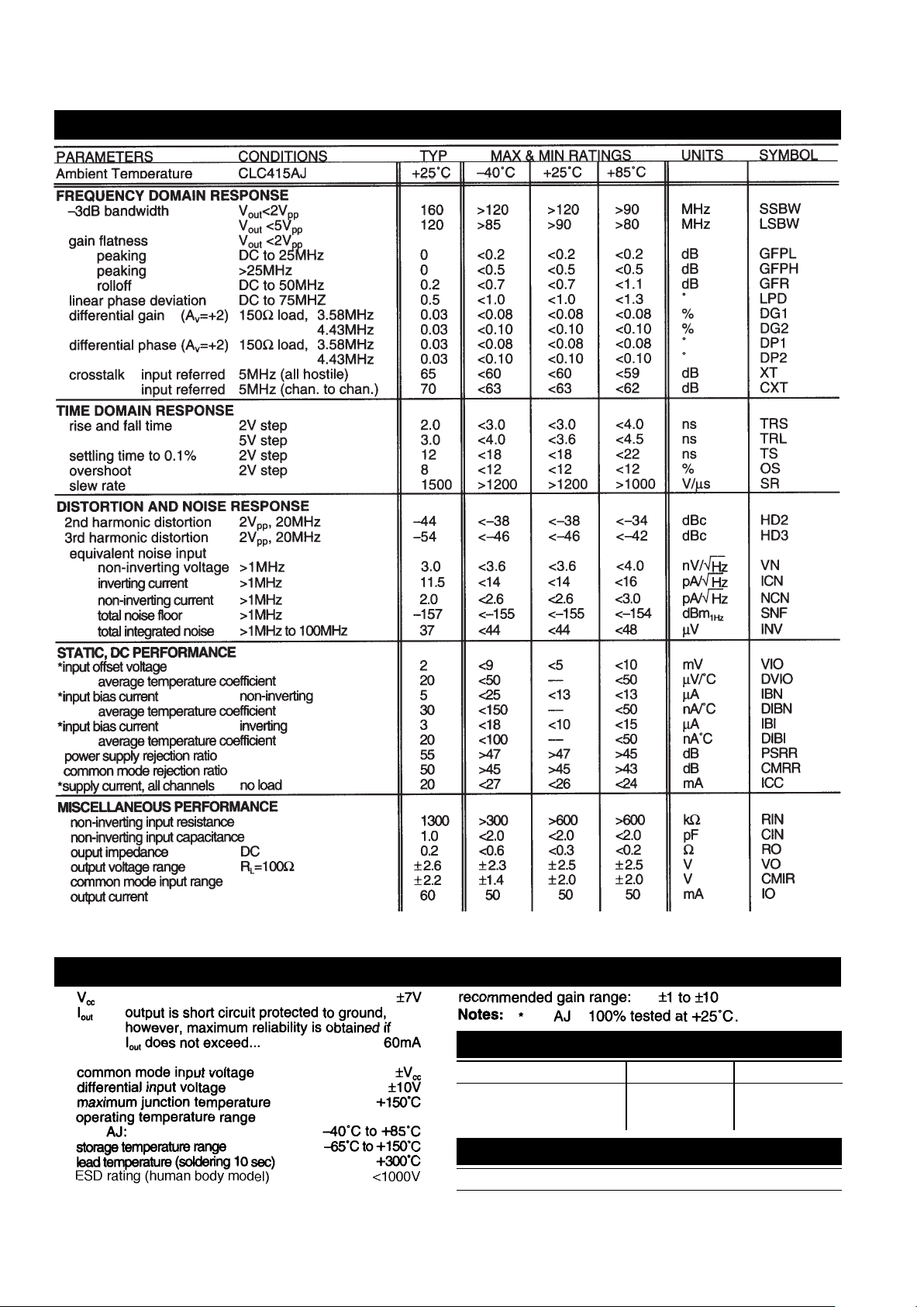
R
f
(Ohms)
|Av|
012345678910
100
200
300
400
500
600
700
800
900
1000
Non-Inverting
Inverting
Page 5

This page intentionally left blank.
5 http://www.national.com
Page 6

CLC415
Quad,Wideband Monolithic Op Amp
http://www.national.com 6
Customer Design Applications Support
National Semiconductor is committed to design excellence. For sales, literature and technical support, call the
National Semiconductor Customer Response Group at 1-800-272-9959 or fax 1-800-737-7018.
Life Support Policy
National’s products are not authorized for use as critical components in life support devices or systems without the express written approval of
the president of National Semiconductor Corporation. As used herein:
1. Life support devices or systems are devices or systems which, a) are intended for surgical implant into the body, or b) support or
sustain life, and whose failure to perform, when properly used in accordance with instr uctions for use provided in the labeling, can
be reasonably expected to result in a significant injury to the user.
2. A critical component is any component of a life support device or system whose failure to perform can be reasonably expected to
cause the failure of the life support device or system, or to affect its safety or effectiveness.
National Semiconductor National Semiconductor National Semiconductor National Semiconductor
Corporation Europe Hong Kong Ltd. Japan Ltd.
1111 West Bardin Road Fax:(+49) 0-180-530 85 86 2501 Miramar Tower Tel: 81-043-299-2309
Arlington, TX 76017 E-mail: europe.support.nsc.com 1-23 Kimberley Road Fax: 81-043-299-2408
Tel: 1(800) 272-9959 Deutsch Tel: (+49) 0-180-530 85 85 Tsimshatsui, Kowloon
Fax:1(800) 737-7018 English Tel: (+49) 0-180-532 78 32 Hong Kong
Francais Tel:(+49) 0-180-532 93 58 Tel: (852) 2737-1600
Italiano Tel: (+49) 0-180-534 16 80 Fax:(852) 2736-9960
National does not assume any responsibility for use of any circuitry described, no circuit patent licenses are implied and National reserves the right at any time without notice to change said
circuitry and specifications.
N
 Loading...