

Page 1
N
CLC412
Dual Wideband Video Op Amp
June 1999
CLC412
Dual Wideband Video Op Amp
General Description
The CLC412 combines a high-speed complementary bipolar process
with National's current-feedback topology to produce a very highspeed dual op amp. The CLC412 provides a 250MHz small-signal
bandwidth at a gain of +2V/V and a 1300V/µs slew rate while
consuming only 50mW per amplifier from ±5V supplies.
The CLC412 offers exceptional video performance with its 0.02%
and 0.02° differential gain and phase errors for NTSC and PAL video
signals while driving one back terminated 75Ω load. The CLC412
also offers a flat gain response of 0.1dB to 30MHz and very low
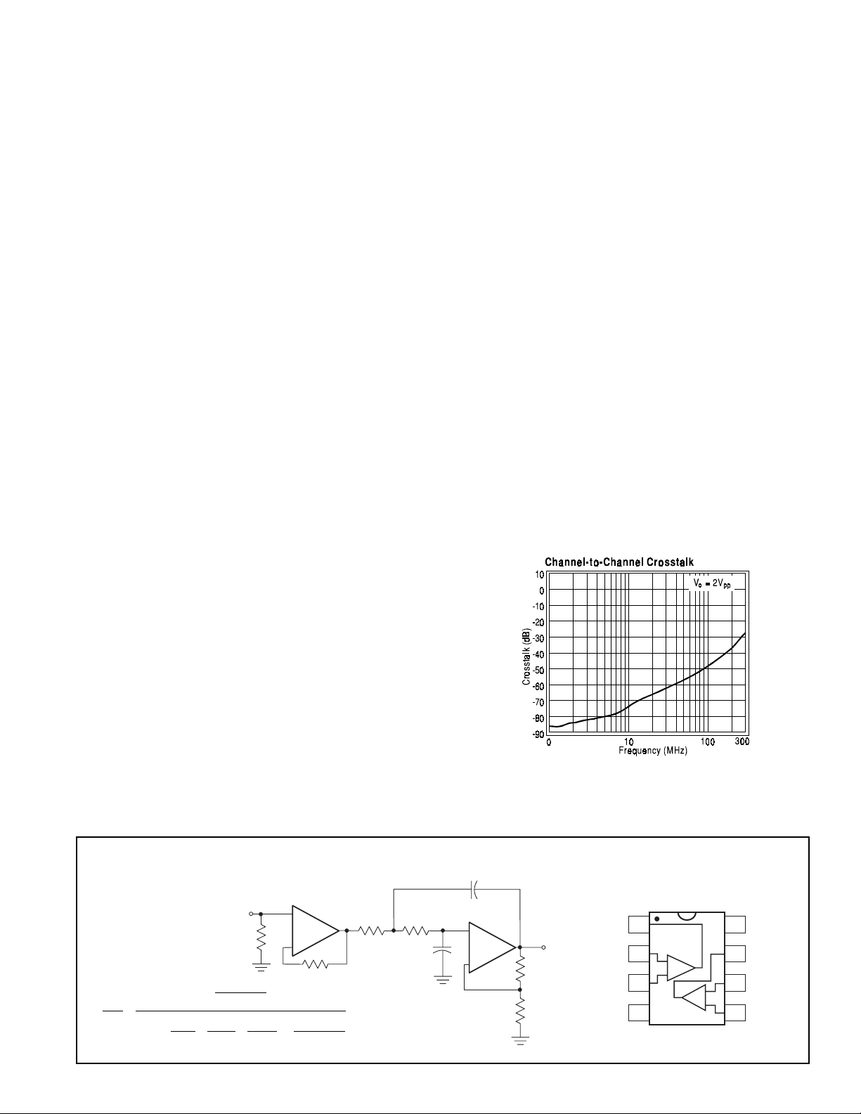
channel-to-channel crosstalk of -76dB at 10MHz. Additionally, each
amplifier can deliver a 70mA continuous output current. This level of
performance makes the CLC412 an ideal dual op amp for highdensity broadcast-quality video systems.
The CLC412's two very well-matched amplifiers support a number of
applications such as differential line drivers and receivers. In
addition, the CLC412 is well suited for Sallen Key active filters in
applications such as anti-aliasing filters for high-speed A/D
converters. Its small 8-pin SOIC package, low power requirement,
low noise and distortion allow the CLC412 to serve portable RF
applications such as IQ-channels.
The CLC412 is available in the following versions.
Features
■ Wide bandwidth: 330MHz (A
250MHz (Av=+2V/V)
■ 0.1dB gain flatness to 30MHz
■ Low power: 5mA/channel
■ Very low diff. gain, phase: 0.02%, 0.02°
■ -76dB channel-to-channel crosstalk
(10MHz)
■ Fast slew rate: 1300V/µs
■ Unity-gain stable
=+1V/V)
v
Applications
■ HDTV, NTSC & PAL video systems
■ Video switching and distribution
■ IQ amplifiers
■ Wideband active filters
■ Cable drivers
■ DC coupled single-to-differential conversions
CLC412AJP -40°C to +85°C 8-pin Plastic DIP
CLC412AJE -40°C to +85°C 8-pin Plastic SOIC
CLC412AIB -40°C to +85°C 8-pin CERDIP
CLC412A8B -55°C to +125°C 8-pin CERDIP,
MIL-STD-883, Level B
CLC412A8L-2A -55°C to +125°C 20-pin LCC,
MIL-STD-883, Level B
CLC412AMC -55°C to +125°C dice,
MIL-STD-883, Level B
DESC SMD number: 5962-94719
Typical Application
Sallen-Key Low-Pass Filter
V
in
V
V
out
=
11
2
in
ss
+++
RC RCKRC RRCC
11 2 2922 1212
K
o
RR CC
1212
1
+
½CLC412
R
in
R
f
−
+
1
R
R
1
2
C
2
C
1
+
½CLC412
-
Pinout
DIP & SOIC
1
1
V
V
non-inv
out
V
inv
-Vcc
2
1
1
+
3
4
+
V
out
R
f
R
g
+V
8
cc
V
out
V
inv
V
non-inv
2
2
2
7
6
5
1999 National Semiconductor Corporation http://www.national.com
Printed in the U.S.A.
Page 2
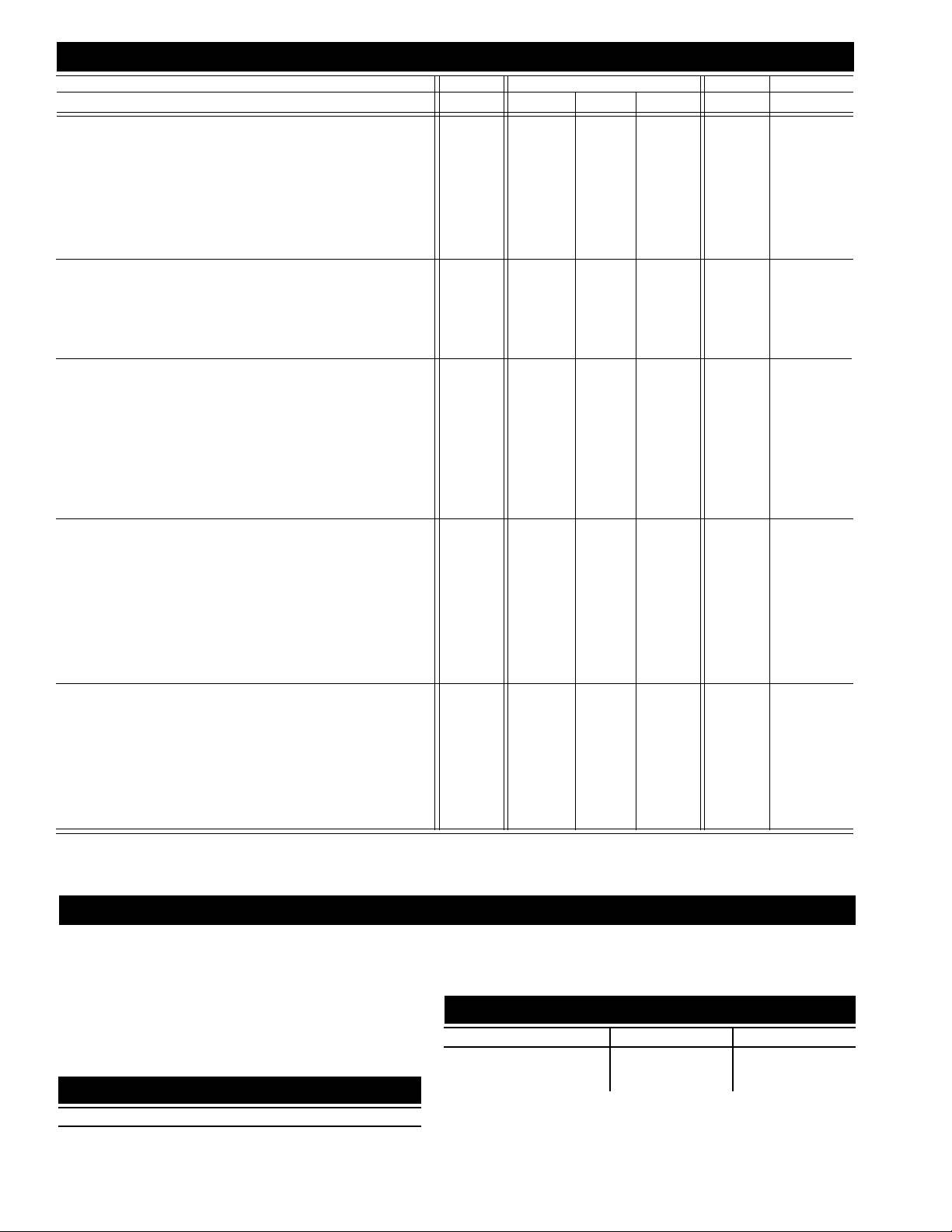
CLC412 Electrical Characteristics (A
= +2; R
V
= 634
f
ΩΩ
Ω; V
ΩΩ
= ±5V; R
CC
= 100
L
ΩΩ
Ω)
ΩΩ
PARAMETERS CONDITIONS TYP MIN/MAX RATINGS UNITS SYMBOL
Ambient Temperature CLC412 AJ +25°C -40°C +25°C +85°C
FREQUENCY DOMAIN RESPONSE
-3dB bandwidth V
gain flatness V
peaking DC to 30MHz 0.1 0.1 0.1 0.2 dB GFP
V
< 0.5V
out
< 4.0V
out
< 0.5V
out
pp
pp
pp
25 0 15 0 175 13 5 M Hz SSBW
10 5 80 80 65 MHz LSBW
rolloff DC to 30MHz 0.1 0.4 0.3 0.3 dB GFR
linear phase deviation DC to 75MHz 0.5 1.3 1.0 1.0 deg LPD
differential gain 4.43MHz, R
differential phase 4.43MHz, R
=150Ω 0.02 0.04 0.04 0.08 % DG
L
=150Ω 0.02 0.04 0.04 0.08 deg DP
L
TIME DOMAIN RESPONSE
rise and fall time 0.5V step 1.4 2.3 2.0 2.6 ns TRS
4V step 3.2 4.4 4.4 4.8 ns TRL
settling time to 0.05% 2V step 12 18 18 20 ns TSS
overshoot 0.5V step 8 15 15 15 % OS
slew rate 2V step 13 00 10 00 1000 800 V/µsSR
DISTORTION AND NOISE RESPONSE
nd
harmonic distortion 2Vpp, 20MHz - 4 6 - 42 - 42 - 38 dBc HD2
2
rd
harmonic distortion 2Vpp, 20MHz - 5 0 - 46 - 46 - 42 dBc HD 3
3
rd
order intermodulation intercept 10MHz 43 dBm
3
1Hz
IMD
equivalent noise input
non-inverting voltage >1MHz 3.0 3.4 3.4 3.8 nV/√Hz VN
inverting current >1MHz 12.0 13.9 13.9 15.5 pA/√Hz NICN
non-inverting current >1MHz 2.0 2.6 2.6 3.0 pA/√Hz ICN
noise floor >1MHz - 1 57 - 156 - 156 - 1 55 dBm
1Hz
SNF
crosstalk input-referred 10MHz - 76 - 70 - 70 - 70 dB XTLKA
STATIC DC PERFORMANCE
*input offset voltage ± 2 ± 1 0 ± 6 ± 12 mV VIO
average drift ± 30 ± 60
*input bias current non-inverting ±5 ± 28 ± 12 ± 12 µAIBN
average drift ± 30 ± 18 7
*input bias current inverting ± 3 ± 3 4 ± 1 5 ± 20 mA IBI
average drift ± 20 ± 12 5
____
____
____
±60 µV/°C DVIO
± 90 nA/°C DIBN
± 80 nA/°C DIBI
power supply rejection ratio DC 50 46 46 44 dB PSRR
common mode rejection ratio D C 50 45 4 5 4 3 d B CMRR
*supply current R
= ∞ 10.2 13.6 12.8 12.8 mA ICC
L
MISCELLANEOUS PERFORMANCE
input resistance non-inverting 1000 300 500 500 kΩ RIN
input capacitance non-inverting 1.0 2.0 2.0 2.0 pF CIN
output resistance closed loop 0.04 0.6 0.3 0.2 Ω ROUT
output voltage range R
= ∞
L
=100Ω
R
L
=100Ω (0° to 70°C)
R
L
+ 3.8,-3.3 +3.6,-2.9 + 3.7,-3.0 + 3.7,-3.0
+ 3.1,-2.9 +2.0,-2.5
± 2.7 ± 2.7 V VOL
+ 2.5,-2.6
VVO
V VOLC
input voltage range common mode ± 2.2 ± 1.4 ± 2.0 ± 2.0 V CMIR
output current 70 25 45 45 mA IO
Min/max ratings are based on product characterization and simulation. Individual parameters are tested as noted. Outgoing quality levels
are determined from tested parameters.
Absolute Maximum Ratings Miscellaneous Ratings
V
cc
I
short circuit protected to ground, however maximum reliabiliy
out
is obtained if I
common-mode input voltage ± V
maximum junction temperature +150°C
operating temperature range: AJ -40°C to +85°C
storage temperature range -65°C to +150°C
lead temperature (soldering 10 sec) +300°C
ESD (100V machine test) 1000V
does not exceed... 125mA
out
Reliability Information
Transistor count 68
http://www.national.com 2
±7V
Recommended gain range ±1 to ±10V/V
Notes:
cc
* AJ : 100% tested at +25°C.
Package Thermal Resistance
Package
AJP 70°C/W 125°C/W
AJE 65°C/W 145°C/W
A8B 40°C/W 130°C/W
θθ
θ
θθ
JC
θθ
θ
θθ
JA
Page 3
3 http://www.national.com
Page 4
http://www.national.com 4
Page 5

+V
cc
+
-
½CLC412
+
-V
cc
R
f
C
3
C
1
V
R
C
2
+
C
4
out
o
+V
cc
C
+
3
C
V
in
R
in
+
½CLC412
-
-V
R
g
1
V
R
C
2
+
C
4
cc
R
f
out
o
V
in
R
g
R
b
Figure 1
Application Introduction
Offered in an 8-pin package for reduced space and cost,
the wideband CLC412 dual current-feedback op amp
provides closely matched DC & AC electrical performance
characteristics making the part an ideal choice for
wideband signal processing. Applications such as
broadcast-quality video systems, IQ amplifiers, filter
blocks, high-speed peak detectors, integrators and
transimpedance amplifiers will all find superior
performance in the CLC412 dual op amp.
Feedback Resistor Selection
The loop gain and frequency response for a currentfeedback operational amplifier is determined largely by
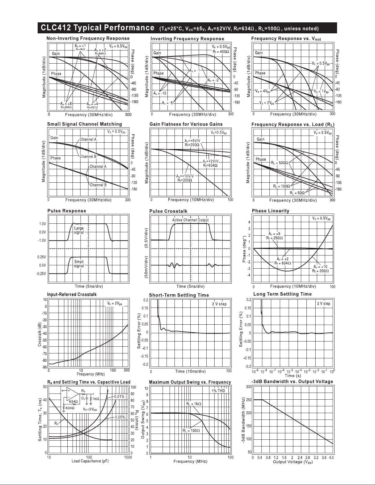
the feedback resistor, Rf. The Electrical Characteristics
and Typical Performance plots specify an Rf of 634Ω, a
gain of +2V/V and operation with ±5V power supplies
(unless otherwise stated). Generally, lowering Rf from its
recommended value will peak the frequency response
and extend the bandwidth while increasing its value will
roll off the response. Reducing the value of Rf too far
below its recommended value will cause overshoot,
ringing and eventually oscillation.
Figure 2
and phase response to the value of the feedback resistor,
Rf. For more information see Application Note OA-13
which describes the relationship between Rf and closedloop frequency response.
When configuring the CLC412 for other inverting or noninverting gains, it is necessary to adjust the value of the
feedback resistor in order to optimize the device’s
frequency and phase response. The two plots below
provide the means of selecting the recommended
feedback-resistor value for both inverting and non-
The plot above labeled "Frequency Response vs. Rf"
shows the CLC412’s frequency and phase response as
Rf is varied while the gain remains constant at +2V/V
(RL=100Ω). This plot shows that one particular value of
Rf will optimize the frequency and phase response at the
specified gain setting, i.e. 634Ω at a gain of +2V/V.
Current-feedback op amps, unlike voltage-feedback op
amps, have a direct relationship between their frequency
inverting gain selections. Both plots show the value of R
approaching a non-zero minimum (dashed line) at high
gains, which is characteristic of current-feedback op
amps, while the linear portion of the two (solid) curves
(i.e. -5>Av>+6) results from the limitation placed on R
(i.e. Rg ≥50Ω). This limitation is due to the desire to keep
Rg greater in value than that of the inverting input
resistance. Therefore, the resulting small-signal
5 http://www.national.com
f
g
Page 6

bandwidth curves, labeled "BW", correspond to the two
(solid) "Rf" curves. These results may deviate from that
produced by the analysis of OA-13 since these plots
were produced from an actual board layout that included
parasitic capacitances not accounted for by the analysis
of OA-13. It should be noted that a non-inverting gain of
+1V/V requires an Rf =1kΩ and the output voltage used
for both plots is 2Vpp.
In order to bandlimit the CLC412 at any particular gain
setting, a larger value of Rf (than previously recommended
in the plots above) is needed. Following the analysis in
OA-13, we find the CLC412’s "optimum feedback
transimpedance", Zt*, below.
∗
ZRR
=+ +
t
f
634 60 1
=+ +
754
=
20 754 57 5Ω.
LOG dB
()
R
f
1
in
R
g
634
634
=
The "optimum feedback transimpedance" is unique for
each current-feedback op amp and determines the
recommended value of Rf for a particular gain setting.
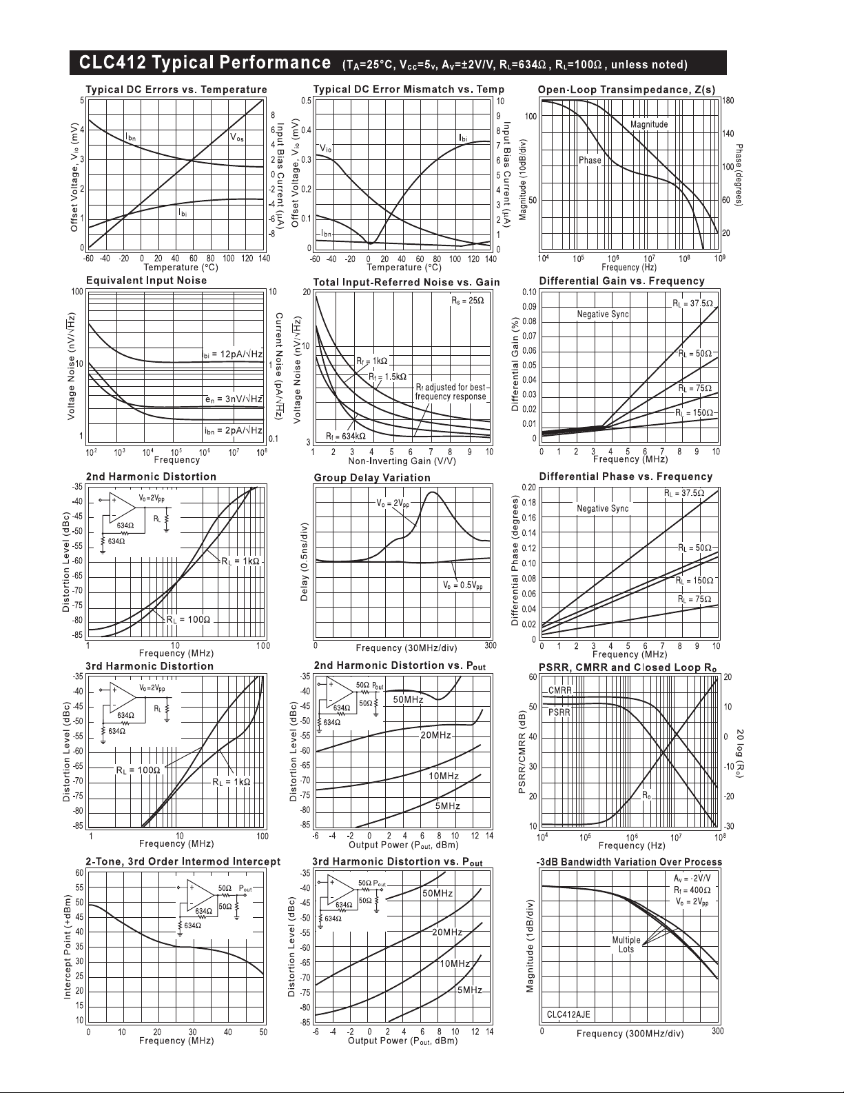
Drawing a horizontal line on the “Open-loop
Transimpedance, Z(s)” plot from 57.5dB (on the left
vertical axis), we find the intersection with the
transimpedance magnitude trace occurs at a frequency
of 180MHz. This frequency is
only an approximation
of
the CLC412’s small-signal bandwidth. From this
intersection, one can see that an increase in Zt will
produce a new intersection occurring at a lower frequency.
This is the process to follow when bandlimiting. Once the
target small-signal bandwidth is determined, the new
value of Zt is picked off the graph at the point where the
this frequency and the transimpedance magnitude trace
intersect. One can then back track to figure the value of
the feedback resistor, Rf=Zt-Rin(1+Rf/Rg). This new value
of Rf will produce the desired frequency roll-off.
surface mount package. Either of these layouts can
assist the designer in obtaining the desired performance.
In addition, the boards can serve as an example layout
for the final production printed circuit board.
Care must also be taken with the CLC412's layout in
order to achieve the best circuit performance, particularly
channel-to-channel isolation. The decoupling capacitors
(both tantalum and ceramic) must be chosen with good
high frequency characteristics to decouple the power
supplies and the physical placement of the CLC412’s
external components is critical. Grouping each amplifier’s
external components with their own ground connection
and separating them from the external components of
the opposing channel with the maximum possible distance
is recommended. The input (Rin) and gain-setting resistors
(Rg) are the most critical. It is also recommended that the
ceramic decoupling capacitor (0.1µF chip or radial-leaded
with low ESR) should be placed as closely to the power
pins as possible.
Package Parasitics
In addition to the parasitic capacitances arising from the
board layout, each of the CLC412's packages has its
own characteristic set of parasitic capacitances and
inductances causing frequency response variation from
package to package as shown in the plot below labeled
"Frequency Response vs. Package Type". Due to its
much smaller size, the CLC412AJE (8-pin SOIC) shows
the least amount of peaking.
Circuit Layout
With all high-frequency devices, board layouts with stray
capacitances have a strong influence over AC
performance. The CLC412 is no exception and its input
and output pins are particularly sensitive to the coupling
of parasitic capacitances (to ac ground) arising from
traces or pads placed too closely (<0.1") to power or
ground planes. In some cases, due to the frequency
response peaking caused by these parasitics, a small
adjustment of the feedback resistor value will serve to
compensate the frequency response. Also, it is very
important to keep the parasitic capacitance across the
feedback resistor to an absolute minimum.
The performance plots in the data sheet can be
reproduced using the evaluation boards available from
Comlinear. There are two types of boards; the DIP
(#730038) and SOIC (#730036). The #730036 board
uses all SMT parts for the evaluation of the CLC412 in its
http://www.national.com 6
Matching Performance
With proper board layout, the AC performance match
between the two CLC412’s amplifiers can be tightly
634Ω
314Ω
V
in
59Ω
25Ω
-
½CLC412
+
+
½CLC412
634Ω
634Ω
50Ω
50Ω
50Ω
50Ω
V
out
Figure 3
Page 7

controlled as shown in Typical Performance plot labeled
“Small-Signal Channel Matching”. The measurements
were performed with SMT components using the
recommended value of feedback resistor of 634Ω at a
gain of +2V/V. The pulse response plot labeled "Pulse
Matching" found below shows the group delay matching
between amplifiers of the CLC412. The circuit topology
is described in Figure 3.
The CLC412's amplifiers, built on the same die, provide
the advantage of having tightly matched DC
characteristics. The typical DC matching specifications
of the CLC412 are:
∆Vio = ±0.60mV, ∆Ibn = ±0.25µA, ∆Ibi = ±1.5µA.
Slew Rate and Settling Time
One of the advantages of current-feedback topology is
an inherently high slew rate which produces a wider fullpower bandwidth. The CLC412 has a typical slew rate of
1300V/µs. The required slew rate for a design can be
calculated by the following equation: SR=2πfV
pk
Careful attention to parasitic capacitances is critical to
achieving the best settling time performance. The CLC412
has a typical short term settling time to 0.05% of 12ns
for a 2 volt step. Also, the amplifier is virtually free of any
long term thermal tail effects at low gains as shown in
the Typical Performance plot labeled “Long Term
Settling Time”.
When measuring settling time, a solid ground plane
should be used in order to reduce ground inductance
which can cause common-ground-impedance coupling.
Power supply and ground trace parasitic capacitances
and the load capacitance will also affect settling time.
Placing a series resistor (Rs) at the output pin is
recommended for optimal settling time performance when
driving a capacitive load. The Typical Performance plot
labeled “Rs and Settling Time vs. Capacitive Load”
provides a means for selecting a value of Rs for a given
capacitive load. The plot also shows the resulting settling
time to 0.05 and 0.01%.
DC & Noise Performance
A current-feedback amplifier’s input stage does not have
equal nor correlated bias currents, therefore they cannot
be canceled and each contributes to the total DC offset
voltage at the output by the following equation:
VIR
offset
=± ∗ +
bn s
R
11
R
g
f
++
V
io
R
R
f
g
+∗
IR
bi
f
The input resistor Rin is the resistance looking from the
non-inverting input back towards the source. For inverting
DC-offset calculations, the source resistance seen by
the input resistor Rg must be included in the output offset
calculation as a part of the non-inverting gain equation.
Application note OA-7 gives several circuits for DC offset
correction. The noise currents for the inverting and noninverting inputs are graphed in the Typical Performance
plot labeled “Equivalent Input Noise”. A more complete
discussion of amplifier input-referred noise and external
resistor noise contribution can be found in OA-12.
Differential Gain & Phase
The CLC412 can drive multiple video loads with very low
differential gain and phase errors. The Typical
Performance plots labeled “Differential Gain vs.
Frequency” and "Differential Phase vs. Frequency" show
performance for loads from 1 to 4. The Electrical
Characteristics table also specifies guaranteed
performance for one 150Ω load at 4.43MHz. For NTSC
video, the guaranteed performance specifications also
apply. Application note OA-08, “Differential Gain and
Phase for Composite Video Systems,” describes in detail
the techniques used to measure differential gain and
phase.
I/O Voltage & Output Current
The usable common-mode input voltage range (CMIR)
of the CLC412 specified in the Electrical Characteristics
table of the data sheet shows a range of ±2.2 volts.
Exceeding this range will cause the input stage to saturate
and clip the output signal.
The output voltage range is determined by the load
resistor and the choice of power supplies. With ±5 volts
the class A/B output driver will typically drive +3.1/-2.7
volts into a load resistance of 100Ω. Increasing the
supply voltages will change the common-mode input and
output voltage swings while at the same time increase
the internal junction temperature. The output voltage for
different load resistors can be determined from the data
sheet plots labeled “Frequency Response vs. Load (RL)"
and “Maximum Output Swing vs. Frequency".
Applications Circuits
Single-to-Differential Line Driver.
The CLC412's well matched AC channel-response allows
a single-ended input to be transformed to highly-matched
push-pull driver. From a 1V single-ended input the circuit
of Figure 4 produces 1V differential signal between the
two outputs. For larger signals, the input voltage divider
(R1=2R2) is necessary to limit the input voltage on channel
2. To achieve the same performance when driving a
matched load, see Figure 3.
7 http://www.national.com
Page 8

R
f
1
R
g
V
in
R
V
in
3
R
1
-
½CLC412
+
1
R
A
v
1
= -0.5V/V
R
o
1
V
out
+
½CLC412
-
2
R
R
g
f
2
2
A
v
2
R
= 1.5V/V
o
2
Figure 4
Differential Line Receiver. Figures 5 and 5a show two
different implementations of an instrumentation amplifier
which convert differential signals to single-ended. Figure
5a allows CMRR adjustment through R2.
R
R
f
--
½CLC412 ½CLC412
++
R
1
RR
(A
+V
in
= -1V/V)
v
1
R
1
-V
in
R
(A
f
= -1V/V)
v
2
V
out
R
1
o
g
CMRR over frequency can be achieved through the
placement of an RC network between the outputs (A and
B) of the two amplifiers of the CLC412.
Non-Inverting Current-Feedback Integrator.
The circuit of Figure 7 achieves its high-speed integration
by placing one of the CLC412's amplifiers in the feedback
loop of the second amplifier configured as shown.
R
R
2
1
R
+
V
in
C
+
½CLC412
-
R
g
½CLC412
VV
=
oin
+
R
b
V
out
R
2
R
1
sRC
Figure 7
Low-Noise Wide-Bandwidth Transimpedance
Amplifier. Figure 8 implements a low-noise
transimpedance amplifier using both channels of the
CLC412. This circuit takes advantage of the lower inputbias-current noise of the non-inverting input and achieves
negative feedback through the second CLC412 channel.
The output voltage is set by the value of Rf while frequency
compensation is achieved through the adjustment of RT.
C
f
Figure 5
R
2
R
f
R
g
R
1
½CLC412
+V
-V
in
= +1
A
v
in
R
R1=R
f
½CLC412
R
Rg=Rf/10
R
f
V
out
R
o
= -10
A
v
Figure 5a
High-Speed Instrumentation Amplifier.
For applications requiring higher CMRR the composite
circuit of Figure 6 uses the two amplifiers of the CLC412
to create balanced inputs for the CLC420 voltagefeedback op amp. The DC CMRR can be fine tuned
through the adjustment of Rb. Further improvement of
V
in
1
V
in
+
R
in
1
½CLC412
-
R
f
1
R
R
f
2
-
½CLC412
+
2
R
in
2
A
R
g
R
a
B
R
f
CLC420
+
R
b
R
in
V
out
R
o
=
R
in
2
1
R
f
+
½CLC412
R
-
+
½CLC412
C
I
s
in
-
R
T
R
g
2
R
A
=−
2
R
R
o
V
o
R
f
2
V
o
f
2
g
2
IR
=
sf
F
I
G
J
1
R
T
G
+
1
)
Z(s
J
ω
A
2
p
G
J
G
J
+
ω
s
H
K
p
Figure 8
Buffered 2nd-Order Sallen-Key Low-Pass Filter.
Figure 9 shows one implementation of a 2nd order
Sallen-Key low pass filter buffered by one of the CLC412's
channels. The CLC412 enables greater precision since
it provides the advantage of very low output impedance
and very linear phase throughout the pass-band.
V
in
+
½CLC412
R
in
-
V
out
=
V
in
2
ss
+++
RC R CKRC RRCC
R
1
R
f
K
o
RR CC
1212
11
11 2 2922 1212
1
−
+
C
R
C
1
2
2
+
½CLC412
-
V
out
R
f
R
g
1
Figure 6
http://www.national.com 8
Figure 9
Page 9

This page intentionally left blank.
9 http://www.national.com
Page 10

This page intentionally left blank.
10 http://www.national.com
Page 11

This page intentionally left blank.
11 http://www.national.com
Page 12

Dual Wideband Video Op Amp
CLC412
Customer Design Applications Support
National Semiconductor is committed to design excellence. For sales, literature and technical support, call the
National Semiconductor Customer Response Group at 1-800-272-9959 or fax 1-800-737-7018.
Life Support Policy
National’s products are not authorized for use as critical components in life support devices or systems without the express written approval
of the president of National Semiconductor Corporation. As used herein:
1. Life support devices or systems are devices or systems which, a) are intended for surgical implant into the body, or b) support or
sustain life, and whose failure to perform, when properly used in accordance with instructions for use provided in the labeling, can
be reasonably expected to result in a significant injury to the user.
2. A critical component is any component of a life support device or system whose failure to perform can be reasonably expected to
cause the failure of the life support device or system, or to affect its safety or effectiveness.
National Semiconductor National Semiconductor National Semiconductor National Semiconductor
Corporation Europe Hong Kong Ltd. Japan Ltd.
1111 West Bardin Road Fax: (+49) 0-180-530 85 86 2501 Miramar Tower Tel: 81-043-299-2309
Arlington, TX 76017 E-mail: europe.support.nsc.com 1-23 Kimberley Road Fax: 81-043-299-2408
Tel: 1(800) 272-9959 Deutsch Tel: (+49) 0-180-530 85 85 Tsimshatsui, Kowloon
Fax: 1(800) 737-7018 English Tel: (+49) 0-180-532 78 32 Hong Kong
National does not assume any responsibility for use of any circuitry described, no circuit patent licenses are implied and National reserves the right at any time without notice to change said
circuitry and specifications.
http://www.national.com 12
Francais Tel: (+49) 0-180-532 93 58 Tel: (852) 2737-1600
Italiano Tel: (+49) 0-180-534 16 80 Fax: (852) 2736-9960
 Loading...