

Page 1
N
CLC411
High-Speed Video Op Amp with Disable
General Description
The CLC411 combines a state-of-the-art complementary bipolar
process with National’s patented current-feedback architecture to
provide a very high-speed op amp operating from ±15V supplies.
Drawing only 11mA quiescent current, the CLC411 provides a
200MHz small signal bandwidth and a 2300V/µs slew rate while
delivering a continuous 70mA current output with ±4.5V output swing.
The CLC411’s high-speed performance includes a 15ns settling time
to 0.1% (2V step) and a 2.3ns rise and fall time (6V step).
The CLC411 is designed to meet the requirements of professional
broadcast video systems including composite video and high definition
television. The CLC411 exceeds the HDTV standard for gain flatness
to 30MHz with it's ±0.05dB flat frequency response and exceeds
composite video standards with its very low differential gain and
phase errors of 0.02%, 0.03°. The CLC411 is the op amp of choice
for all video systems requiring upward compatibility from NTSC and
PAL to HDTV.
The CLC411 features a very fast disable/enable (10ns/55ns) allowing
the multiplexing of high-speed signals onto an analog bus through the
common output connections of multiple CLC411’s. Using the same
signal source to drive disable/enable pins is easy since “breakbefore-make” is guaranteed.
The CLC411 is available in several versions:
CLC411AJP -40°C to +85°C 8-pin plastic DIP
CLC411AJE -40°C to +85°C 8-pin plastic SOIC
CLC411A8B -55°C to +125°C 8-pin hermetic CERDIP,
MIL-STD-883
CLC411AMC -55°C to +125°C dice, MIL-STD-883, Level B
DESC SMD number: 5962-94566
June 1999
CLC411
High-Speed Video Op Amp with Disable
Features
■ 200MHz small signal bandwidth (1V
pp
)
■ ±0.05dB gain flatness to 30MHz
■ 0.02%, 0.03° differential gain, phase
■ 2300V/µs slew rate
■ 10ns disable to high-impedance output
■ 70mA continuous output current
■ ±4.5V output swing into 100Ω load
■ ±4.0V input voltage range
Applications
■ HDTV amplifier
■ Video line driver
■ High-speed analog bus driver
■ Video signal multiplexer
■ DAC output buffer
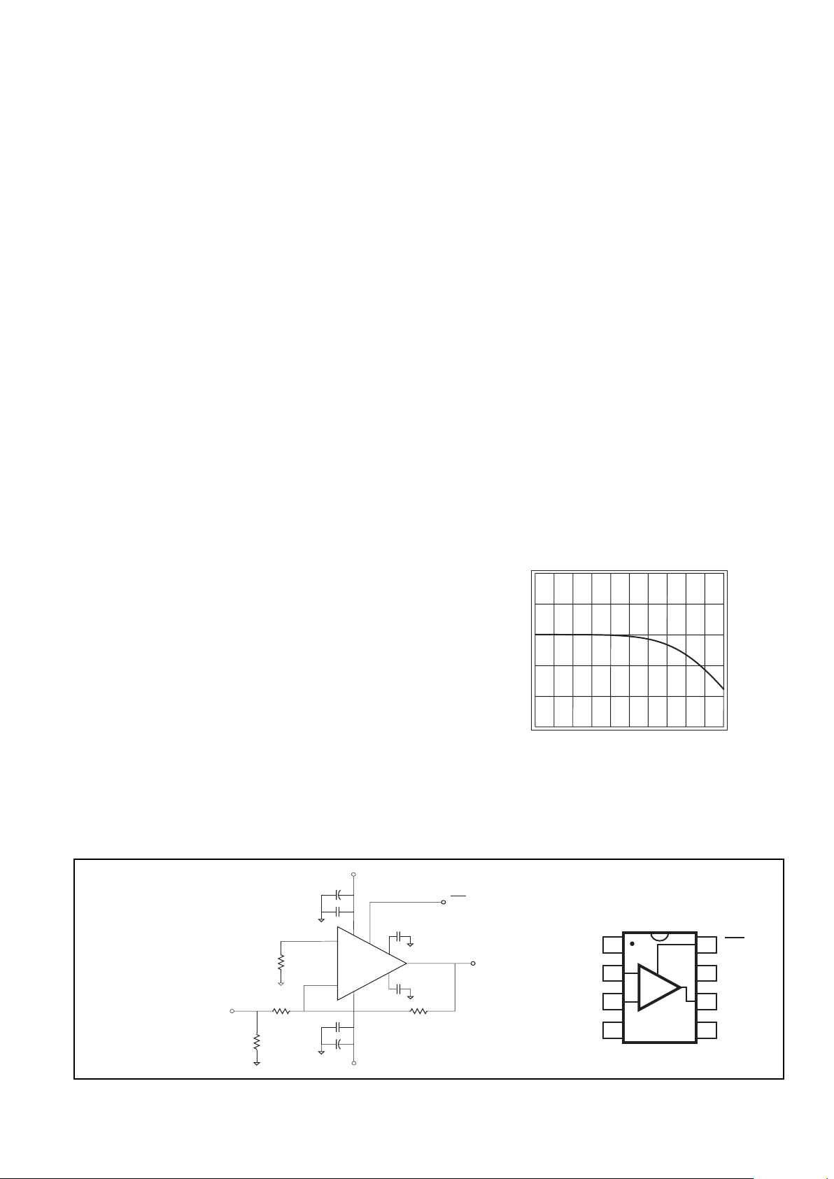
Pinout
DIP & SOIC
0.01µF
0.1µF
0.1µF
6.8µF
6.8µF
0.01µF
+V
r
-V
r
V
in
+
_
3
2
4
7
8
1
5
6
CLC411
25Ω
R
T
R
g
Select RTto yield
Rin=RT||R
g
R
f
V
out
DIS
-V
cc
+V
cc
Recommended
Inverting Gain
Configuration
0 Frequency (5MHz/div) 50
Magnitude (0.5dB/div)
Gain Flatness (Av=+2)
-
+
1
2
3
4
DIS
+V
cc
V
out
-V
r
+V
r
V
inv
V
non-inv
-V
cc
8
7
6
5
1999 National Semiconductor Corporation http://www.national.com
Printed in the U.S.A.
Page 2
PARAMETERS CONDITIONS TYP MIN/MAX RATINGS UNITS SYMBOL
Ambient Temperature CLC411 AJ +25
°
C -40°C +25°C +85°C
FREQUENCY DOMAIN RESPONSE
-3dB bandwidth V
out
< 1V
pp
20 0 15 0 150 110 MH z SSBW
V
out
< 6V
pp
75 50 50 40 MHz LSBW
gain flatness V
out
< 1V
pp
peaking DC to 30MHz 0.05 0.2 0.2 0.3 dB GFPL
rolloff DC to 30MHz 0.05 0.2 0.2 0.4 dB GFRL
peaking DC to 200MHz 0.1 0. 6 0.5 0. 6 d B GFPH
rolloff DC to 60MHz 0.2 0.7 0.4 0. 7 d B GFRH
linear phase deviation DC to 60MHz 0.3 1.0 1.0 1.0 ° LPD
differential gain 4.43MHz, R
L
=150W 0.02 % DG
differential phase 4.43MHz, RL=150W 0.03 ° DP
TIME DOMAIN RESPONSE
rise and fall time 6V step 2 .3 ns TR
settling time to 0.1% 2V step 15 23 18 23 ns TS
overshoot 2V step 5 15 10 15 % OS
slew rate 6V step 23 00 V/µsSR
DISTORTION AND NOISE RESPONSE (note 1)
2
ND
harmonic distortion 2Vpp, 20MHz -48 -35 -35 -35 dBc HD2
3
RD
harmonic distortion 2Vpp, 20MHz -52 -42 -42 -35 dBc HD3
equivalent noise input
voltage >1MHz 2.5 nV/√Hz VN
inverting current >1MHz 12.9 pA/√Hz ICI
non-inverting current >1MHz 6.3 pA/√Hz ICN
noise floor >1MHz -157 dBm
1Hz
SNF
integrated noise 1MHz to 200MHz 45 µVINV
STATIC DC PERFORMANCE
*input offset voltage ±2 ±13 ±9.0 ±1 4 mV VIO
average temperature coefficient +30 ± 50
____
±50 µV/°C DVIO
*input bias current non-inverting 12 65 30 ±20 µAIBN
average temperature coefficient ±200 ±400
____
±250 nA/°C DIBN
*input bias current inverting ±1 2 ±40 ±30 ±30 µA IBI
average temperature coefficient ±50 ±200
____
±150 nA/°C DIBI
power supply rejection ratio 56 48 50 48 dB PSRR
common mode rejection ratio 52 44 46 44 dB CMRR
*supply current no load 1 1 14 12 12 mA ICC
supply current disabled 2.5 4.5 3.5 4.5 mA ICCD
DISABLE/ENABLE PERFORMANCE (note 2)
disable time to >50dB attenuation @10MHz 10 3 0 30 60 ns TOFF
enable time 55 ns TON
DIS voltage pin 8
to disable 4.5 <3.0 <3.0 <3.0 V VDIS
to enable 5.5 >7.0 >6.5 >6.5 V VEN
off isolation at 10MHz 59 5 5 5 5 55 dB OSD
MISCELLANEOUS PERFORMANCE
non-inverting input resistance 100 0 250 7 50 1000 kΩ RIN
non-inverting input capacitance 2.0 3.0 3.0 3.0 pF CIN
output voltage range no load ±6.0 ±4.5 V VO
output voltage range R
L
=100Ω ±4.5 ±4.0 V VOL
common mode input range ±4.0 ±3.5 V CMIR
output current 70 30 50 40 mA IO
Min/max ratings are based on product characterization and simulation. Individual parameters are tested as noted. Outgoing quality levels
are determined from tested parameters.
CLC411 Electrical Characteristics
(A(A
(A(A
(A
VV
VV
V
= +2; V= +2; V
= +2; V= +2; V
= +2; V
CCCC
CCCC
CC
= =
= =
=
±±
±±
±
15V; R15V; R
15V; R15V; R
15V; R
LL
LL
L
= 100= 100
= 100= 100
= 100
ΩΩ
ΩΩ
Ω
; R; R
; R; R
; R
ff
ff
f
= 301= 301
= 301= 301
= 301
ΩΩ
ΩΩ
Ω
, unless noted), unless noted)
, unless noted), unless noted)
, unless noted)
Absolute Maximum Ratings
Miscellaneous Ratings
V
cc
±18V
I
out
125mA
common-mode input voltage ±V
cc
differential input voltage ±15V
maximum junction temperature +150°C
operating temperature range: AJ -40°C to +85°C
storage temperature range -65°C to +150°C
lead temperature (soldering 10 sec) +300°C
ESD (human body model) 1000V
Recommended gain range ±1 to ±10V/V
Notes: * AJ :100% tested at +25°C.
note 1 : Specifications guaranteed using 0.01mF bypass capacitors
on pins 1 & 5.
note 2 : Break before make is guaranteed.
http://www.national.com 2
Package Thermal Resistance
Package
θθ
θθ
θ
JC
θθ
θθ
θ
JA
AJP 65°C/W 120°C/W
AJE 55°C/W 135°C/W
A8B 25°C/W 115°C/W
Reliability Information
Transistor count 70
Page 3
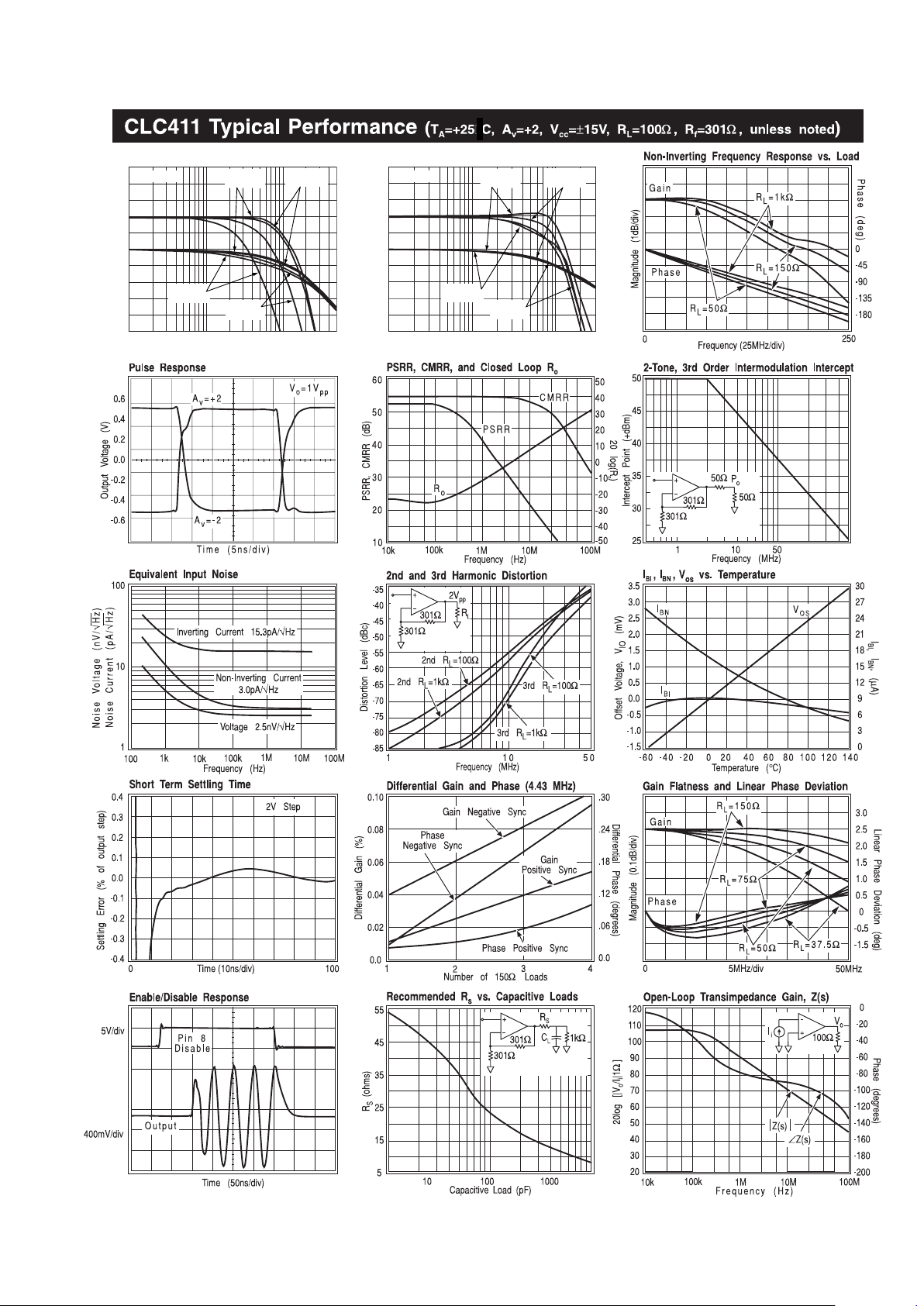
Inverting Frequency Response
Magnitude (1dB/div)
Frequency (MHz)
1
10
100
Phase (deg)
-270
-540
-360
-450
-180
-630
V
out
= 1V
pp
Av = -2
Rf = 301Ω
Av = -1
Rf = 301Ω
Av = -10
Rf = 200Ω
Av = -5
Rf = 249Ω
Non-Inverting Frequency Response
Magnitude (1dB/div)
Frequency (MHz)
1
10
100
Phase (deg)
-90
-360
-180
-270
0
-450
V
out
= 1V
pp
Av = 2
Rf = 301Ω
Av = 1
R
f
= 402Ω
Av = 10
Rf = 200Ω
Av = 5
Rf = 200Ω
Frequency (MHz)
Frequency (MHz)
o
3 http://www.national.com
Page 4

Description
The CLC411 is a high-speed current-feedback operational
amplifier which operates from ±15V power supplies.
The external supplies (±VCC) are regulated to lower
voltages internally. The amplifier itself sees
approximately ±6.5V rails. Thus the device yields
performance comparable to Comlinear’s ±5V devices,
but with higher supply voltages. There is no degradation
in rated specifications when the CLC411 is operated
from ±12V. A slight reduction in bandwidth will be
observed with ±10V supplies. Operation at less than
±10V is not recommended.
A block diagram of the amplifier and regulator topology
is shown in Figure 2, “CLC411 Equivalent Circuit.” The
regulators derive their reference voltage from an internal
floating zener voltage source. External control of the
zener reference pins can be used to level-shift amplifier
operation which is discussed in detail in the section
entitled “Extending Input/Output Range with Vr.”
Power Supply Decoupling
There are four pins associated with the power supplies.
The VCC pins (4,7) are the external supply voltages. The
Vr pins (5,1) are connected to internal reference nodes.
Figures 1 and 3 , “Recommended Non-inverting Gain
Circuit” and "Recommended Inverting Gain Circuit"
show the recommended supply decoupling scheme
with four ceramic and two electrolytic capacitors. The
ceramic capacitors must be placed immediately adjacent
to the device pins and connected directly to a good
0.01µF
0.1µF
0.1µF
6.8µF
6.8µF
0.01µF
+V
r
-V
r
V
in
+
_
3
2
4
7
8
1
5
6
CLC411
R
in
R
g
R
f
V
out
DIS
+V
cc
-V
cc
0.01µF
0.1µF
0.1µF
6.8µF
6.8µF
0.01µF
+V
r
-V
r
V
in
+
_
3
2
4
7
8
1
5
6
CLC411
25Ω
R
T
R
g
Select RTto yield
R
in
=RT||R
g
R
f
V
out
DIS
-V
cc
+V
cc
Figure 3: Recommended
Inverting Gain Circuit
Figure 1: Recommended
Non-inverting Gain Circuit
low-inductance ground plane. Bypassing the Vr pins will
reduce high frequency noise (>10MHz) in the amplifier.
If this noise is not a concern these capacitors may be
eliminated.
Differential Gain and Phase
The differential gain and phase errors of the CLC411
driving one doubly-terminated video load (RL=150Ω) are
specified and guaranteed in the “Electrical
Characteristics” table. The “Typical Performance” plot,
“Differential Gain and Phase (4.43MHz)” shows the
differential gain and phase performance of the CLC411
when driving from one to four video loads. Application
note OA-08, “Differential Gain and Phase for Composite
Video Systems,” describes in detail the techniques
used to measure differential gain and phase.
Feedback Resistor
The loop gain and frequency response for a currentfeedback operational amplifier is determined largely by
the feedback resistor, Rf. The electrical characteristics
and typical performance plots contained within the
datasheet, unless otherwise stated, specify an Rf of
301Ω, a gain of +2V/V and operation with ±15V power
supplies. The frequency response at different gain
settings and supply voltages can be optimized by
selecting a different value of Rf. Generally, lowering R
f
will peak the frequency response and extend the
bandwidth while increasing its value will roll off the
response. For unity-gain voltage follower circuits, a
Figure 4: Recommended Rf vs. Gain
Figure 2: CLC411 Equivalent Circuit
17kΩ
1
7
5
4
3
2
6
17kΩ
+V
cc
+V
r
V
z
-V
r
-V
cc
+
-
+
-
+
reg
_
reg
http://www.national.com 4
R
f
(Ω)
Gain (V/V)
500
400
300
200
100
0
0123456789
10
Non-Inverting
Inverting
Page 5

Figure 5C: ECL Interface
Figure 5B: Differential ECL Interface
Figure 5A: Disable Interface
Q3
+15V
-15V
3.57kΩ
Q1
Q4
Q2Disable
CLC411 pin 8, DISABLE
V
th
330Ω
-5.2V
ECL
Gate
-5.2V
330Ω
Q1 Q2
Q1,Q2 MPSH10
Q3,Q4 MPSH81
0.1µF
0.1µF
0.1µF
-15V
-5.2V
10kΩ
330Ω
931Ω
Q1
ECL
Gate
Q2
0.1µF
1N914
332Ω
TTL
Gate
50Ω
50Ω
50Ω
Q1
Q2
non-zero Rf must be used with current-feedback
operational amplifiers such as the CLC411. Application
note OA-13, “Current-Feedback Loop-Gain Analysis
and Performance Enhancements,” explains the
ramifications of Rf and how to use it to tailor the desired
frequency response with respect to gain. The equations
found in the application note should be considered as a
starting point for the selection of Rf. The equations do
not factor in the effects of parasitic capacitance found
on the inverting input, the output nor across the feedback
resistor. Equations in OA-13 require values for R
f
(301Ω), Av (+2) and Ri (inverting input resistance, 50Ω).
Combining these values yields a Zt* (optimum feedback
transimpedance) of 400Ω. Figure 4 entitled
"Recommended Rf vs. Gain" will enable the selection of
the feedback resistor that provides a maximally flat
frequency response for the CLC411 over its gain range.
The linear portion of the two curves (i.e. AV>4) results
from the limitation on Rg (i.e. Rg ≥50Ω).
Enable/Disable Operation
The disable feature allows the outputs of several CLC411
devices to be connected onto a common analog bus
forming a high-speed analog multiplexer. When disabled,
the output and inverting inputs of the CLC411 become
high impedances. The disable pin has an internal pullup resistor which is pulled-up to an internal voltage, not
to the external supply. The CLC411 is enabled when pin
8 is left open or pulled-up to ≥+7V and disabled when
grounded or pulled below +3V. CMOS logic devices are
necessary to drive the disable pin. For example, CMOS
logic with VDD ≥ +7V will guarantee proper operation over
temperature. TTL voltage levels are inadequate for
controlling the disable feature.
For faster enable/disable operation than 15V CMOS
logic devices will allow, the circuit of Figure 5 is
recommended. A fast four-transistor comparator, Figure
5A, interfaces between the CLC411 DISABLE pin and
several standard logic families. This circuit has a
differential input between the bases of Q1 and Q2. As
such it may be driven directly from differential ECL
logic, as in shown in Figure 5B. Single-ended logic
families may also be used by establishing an appropriate
threshold voltage on the Vth input, the base of Q2.
Figures 5C and 5D illustrate a single-ended ECL and
TTL interface respectively. The Disable input, the base
of Q1, is driven above and below the threshold, Vth.
Fastest switching speeds result when the differential
voltage between the bases of Q1 and Q2 is kept to less
A
B
C
0
1
2
3
4
5
6
7
+
A
CLC411
CLC411
DIS (pin 8)
Buffers
DIS (pin 8)
-
+
B
-
Analog Bus
Figure 6: General Multiplexing Circuit
5 http://www.national.com
Figure 5D: TTL Interface
Page 6

than one volt. Single-ended ECL, Figure 5C, maintains
this desired maximum differential input voltage. TTL
and CMOS have higher V
high
to V
low
excursions. The
circuit of figure 5D will ensure the voltage applied
between the bases of Q1 and Q2 does not cause
excessive switching delays in the CLC411. Under the
above proscribed four-transistor interface, all variations
were evaluated with approximately 1ns rise and fall
times which produced switching speeds equivalent to
the rated disable/enable switching times found in the
"CLC411 Electrical Characteristics" table.
A general multiplexer configuration using several
CLC411s is illustrated in figure 6, where a typical 8-to1 digital mux is used to control the switching operation
of the paralleled CLC411s. Since "break-before-make"
is a guaranteed specification of the CLC411 this
configuration works nicely. Notice the buffers used in
driving the disable pins of the CLC411s. These buffers
may be 15V CMOS logic devices mentioned previously
or any variation of the four-transistor comparator
illustrated above.
Extending Input/Output Range with V
r
As can be seen in Figure 3, the magnitude of the internal
regulated supply voltages is fixed by Vz. In normal
operation, with ±15V external supplies, +Vr is nominally
+
9V when left floating. CMIR (common mode input
range) and VO (output voltage range, no load) are
specified under these conditions. These parameters
implicitly have 0V as their midpoint, i.e. the VO range
is ±6V, centered at 0V.
An external voltage source can be applied to +Vr to shift
the range of the input/output voltages. For example, if
it were desired to move the positive VO range from +6V
to a +9V maximum in unipolar operation, Figure 7, “DC
Parameters as a Function of +Vr”, is used to determine
the required supply and +Vr voltages. Referring to
Figure 7, locate the point on the +VO
MAX
line where the
ordinate is +9V. Draw a vertical line from this point
intersecting the other lines in the graph. The circuit
voltages are the ordinates of these intersections. For
this example these points are shown in the graph as
solid dots. The required voltage sources are +Vr=+12V,
+
VCC=+12V, -VCC=-12V. When these supply and
reference voltages are applied, the range for VO is -3V
to +9V, and CMIR ranges from -1V to +7V. The difference
between the minimum and maximum voltages is
constant, i.e. 12V for VO, only the midpoint has been
shifted, i.e. from 0V to +3V for VO.
Note that in this example the -Vr pin has been left open
(or bypassed to reduce high-frequency noise). The
difference between +Vr and -Vr is fixed by Vz. A levelshifting voltage can be applied to only one of the
reference pins, not both. If extended operation were
needed in the negative direction, Figure 4 may be used
by changing the signs, and applying the resultant
negative voltage to the -Vr pin. It is recommended that
+
Vr be used for positive shifts, and -Vr for negative
shifts of input/output voltage range.
Printed Circuit Layout & Evaluation Board
Refer to application note OA-15, “Frequent Faux Pas in
Applying Wideband Current Feedback Amplifiers,” for
board layout guidelines and construction techniques. Two
very important points to consider before creating a layout
which are found in the above application note are worth
reiteration. First the input and output pins are sensitive to
parasitic capacitances. These parasitic capacitances
can cause frequency-response peaking or sustained
oscillation. To minimize the adverse effect of parasitic
capacitances, the ground plane should be removed from
those pins to a distance of at least 0.25" Second, leads
should be kept as short as possible in the finished layout.
In particular, the feedback resistor should have its shortest
lead on the inverting input side of the CLC411. The output
is less sensitive to parasitic capacitance and therefore
can drive the longer of the two feedback resistor
connections. The evaluation board available for the CLC411
(part #730013 for through-hole packages, 730027 for SO-
8) may be used as a reference for proper board layout.
Application schematics for this evaluation board are in the
product accessories section of the Comlinear databook.
Figure 7: DC Parameters as a Function of +V
r
51015-10 -5
Recommended
+Vcc range
Recommended
-Vcc range
20
15
10
5
-5
-10
-15
+V
CC
max
+V
r
+VO
max
-VO
min
V
cm
+
V
cm
_
-V
CC
max
http://www.national.com 6
Page 7

This page intentionally left blank.
7 http://www.national.com
Page 8

CLC411
High-Speed Video Op Amp with Disable
http://www.national.com
8
Customer Design Applications Support
National Semiconductor is committed to design excellence. For sales, literature and technical support, call the
National Semiconductor Customer Response Group at 1-800-272-9959 or fax 1-800-737-7018.
Life Support Policy
National’s products are not authorized for use as critical components in life support devices or systems without the express written approval
of the president of National Semiconductor Corporation. As used herein:
1. Life support devices or systems are devices or systems which, a) are intended for surgical implant into the body, or b) support or
sustain life, and whose failure to perform, when properly used in accordance with instructions for use provided in the labeling, can
be reasonably expected to result in a significant injury to the user.
2. A critical component is any component of a life support device or system whose failure to perform can be reasonably expected to
cause the failure of the life support device or system, or to affect its safety or effectiveness.
National Semiconductor National Semiconductor National Semiconductor National Semiconductor
Corporation Europe Hong Kong Ltd. Japan Ltd.
1111 West Bardin Road Fax: (+49) 0-180-530 85 86 2501 Miramar Tower Tel: 81-043-299-2309
Arlington, TX 76017 E-mail: europe.support.nsc.com 1-23 Kimberley Road Fax: 81-043-299-2408
Tel: 1(800) 272-9959 Deutsch Tel: (+49) 0-180-530 85 85 Tsimshatsui, Kowloon
Fax: 1(800) 737-7018 English Tel: (+49) 0-180-532 78 32 Hong Kong
Francais Tel: (+49) 0-180-532 93 58 Tel: (852) 2737-1600
Italiano Tel: (+49) 0-180-534 16 80 Fax: (852) 2736-9960
National does not assume any responsibility for use of any circuitry described, no circuit patent licenses are implied and National reserves the right at any time without notice to change said
circuitry and specifications.
N
 Loading...