

Page 1
Frequency Response (AV = +2V/V)
Features
■
Low-cost
■
High output current: 60mA
■
High input impedance: 6MΩ
■
Gains of +1, +2 with no external components
■
Low power: Icc= 3.5mA
■
Ultra-fast enable/disable times
■
Very low input bias currents: 100nA
■
Excellent gain accuracy: 0.1%
■
High speed: 110MHz -3dB BW
Applications
■
Desktop video systems
■
Multiplexers
■
Video distribution
■
Flash A/D driver
■
High-speed switch/driver
■
High-source impedance applications
■
Peak detector circuits
■
Professional video processing
■
High resolution monitors
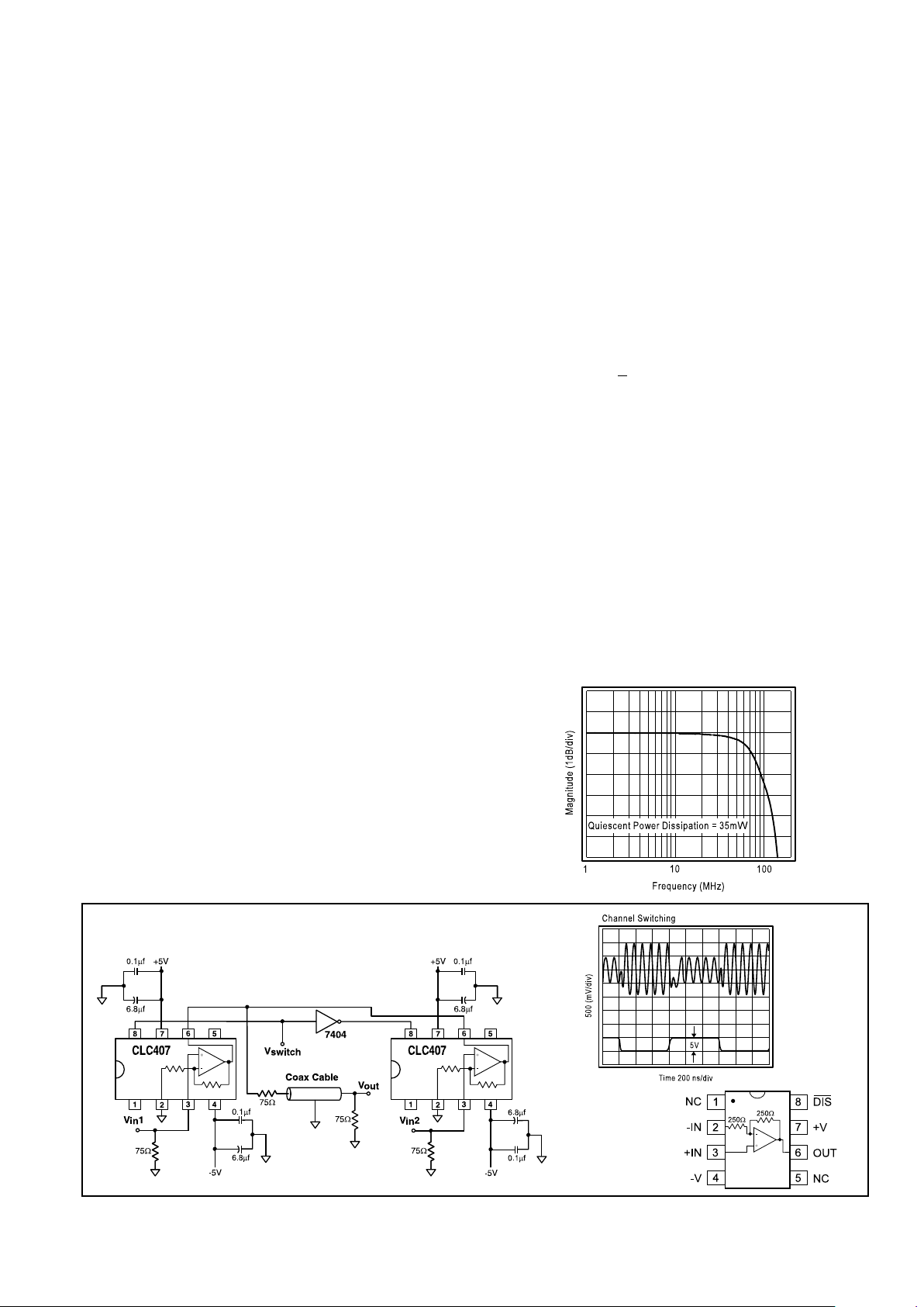
NOTE: All necessary components are shown.
Typical Application
2:1 Mux Cable Driver
Pinout
DIP & SOIC
General Description
The Comlinear CLC407 is a low-cost, high-speed (110MHz)
buffer which features user-programmable gains of +2, +1, and -1
V/V. This high-performance part has the added versatility of a
TTL-compatible disable which quickly switches the buffer off in
18ns and back on in 40ns. The CLC407’s high 60mA output
current, coupled with its ultra-low 35mW power consumption
makes it the ideal choice for demanding applications that are
sensitive to both power and cost.
Utilizing Comlinear’s proven architectures, this current feedback
amplifier surpasses the performance of alternate solutions with a
closed-loop design that produces new standards for buffers in
gain accuracy, input impedance, and input bias currents. The
CLC407’s internal feedback network provides an excellent gain
accuracy of 0.1%. High source impedance applications will
benefit from the CLC407’s 6MΩ input impedance along with its
exceptionally low 100nA input bias current.
With 0.1dB flatness to 30MHz and low differential gain and phase
errors, the CLC407 is very useful for professional video processing and distribution. A 110MHz -3dB bandwidth coupled with a
350V/µs slew rate also make the CLC407 a perfect choice in
cost-sensitive applications such as video monitors, fax machines,
copiers, and CATV systems. Back-terminated video applications
will especially appreciate +2 gains which require no external gain
components reducing inventory costs and board space.
Comlinear CLC407
Low-Cost, Low-Power
Programmable Gain Buffer with Disable
N
August 1996
Comlinear CLC407
Low-Cost, Low-Power, Programmable Gain Buffer with Disable
© 1996 National Semiconductor Corporation http://www.national.com
Printed in the U.S.A.
Page 2
PARAMETERS CONDITIONS TYP MIN/MAX RATINGS UNITS NOTES
Ambient Temperature CLC407AJ +25˚C +25˚C 0 to 70˚C -40 to 85˚C
FREQUENCY DOMAIN RESPONSE
-3dB bandwidth V
out
< 1.0V
pp
110 75 50 45 MHz B
V
out
< 5.0V
pp
42 31 27 26 MHz 1
±
0.1dB bandwidth V
out
< 1.0V
pp
30 15 MHz
gain flatness V
out
< 1.0V
pp
peaking DC to 200MHz 0 0.4 0.6 0.8 dB B
rolloff <30MHz 0.1 0.5 0.65 0.7 dB B
linear phase deviation <20MHz 0.3 0.6 0.7 0.7 deg
differential gain NTSC, RL=150Ω 0.03 0.05 0.06 0.07 %
NTSC, RL=150Ω
(Note 2)
0.01 % 2
differential phase NTSC, RL=150Ω 0.25 0.4 0.5 0.55 deg
NTSC, RL=150Ω
(Note 2)
0.08 deg 2
TIME DOMAIN RESPONSE
rise and fall time 2V step 5 7.5 8.2 8.4 ns
settling time to 0.05% 2V step 18 27 36 39 ns
overshoot 2V step 3 12 12 12 %
slew rate AV = +2 2V step 350 260 225 215 V/µs
AV = -1 1V step 650 V/µs
DISTORTION AND NOISE RESPONSE
2nd harmonic distortion 2Vpp, 1MHz/10MHz -72/-52 -46 -45 -44 dBc B, C
3rd harmonic distortion 2V
pp
, 1MHz/10MHz -70/-57 -50 -47 -46 dBc B, C
equivalent input noise
non-inverting voltage >1MHz 5 6.3 6.6 6.7 nV/√Hz
inverting current >1MHz 12 15 16 17 pA/√Hz
non-inverting current >1MHz 3 3.8 4 4.2 pA/√Hz
STATIC DC PERFORMANCE
input offset voltage 1 5 7 8 mV
average drift 30 50 50 µV/˚C
input bias current non-inverting 100 900 1600 2800 nA A
average drift 3 8 11 nA/˚C
input bias current inverting 1 5 6 8 µA
average drift 17 40 45 nA/˚C
output offset voltage 2.5 13 17 19 mV A,3
amplifier gain error
±
0.1%
±
1.0%
±
1.0%
±
1.0% V/V A
internal feedback resistor (R
f
) 250
±
20% Ω
power supply rejection ratio DC 52 47 46 45 dB B
common-mode rejection ratio DC 50 45 44 43 dB
supply current R
L
= ∞ 3.5 4.0 4.1 4.4 mA A
disabled R
L
= ∞ 0.8 0.9 0.95 1 mA A
SWITCHING PERFORMANCE
turn on time 40 55 58 58 ns
turn off time to >50dB attn. @ 10MHz 18 26 30 32 ns
off isolation 10MHz 85 80 80 80 dB
high input voltage V
IH
222V
low input voltage V
IL
0.8 0.8 0.8 V
MISCELLANEOUS PERFORMANCE
input resistance non-inverting 6 3 2.4 1 MΩ
input capacitance non-inverting 1 2 2 2 pF
common mode input range ±2.2 1.8 1.7 1.5 V
output voltage range R
L
= ∞ +4.0,-3.3 +3.9,-3.2 +3.8,-3.1 +3.7,-2.8 V
output current 60 44 38 20 mA
output resistance, closed loop 0.06 0.2 0.25 0.4 Ω
Recommended gain range +1, +2 V/V
Min/max ratings are based on product characterization and simulation. Individual parameters are tested as noted. Outgoing quality levels are
determined from tested parameters.
CLC407 Electrical Characteristics
(AV= +2, Vcc= + 5V, RL= 100Ω unless specified)
Absolute Maximum Ratings
supply voltage
±
7V
I
out
is short circuit protected to ground
common-mode input voltage
±
Vcc
maximum junction temperature +175˚C
storage temperature range -65˚C to +150˚C
lead temperature (soldering 10 sec) +300˚C
Notes
1) At temps < 0˚C, spec is guaranteed for RL= 500Ω.
2) An 825Ω pull-down resistor is connected between V
o
and -Vcc.
3) Source impedance 1kΩ.
A) J-level: spec is 100% tested at +25˚C, sample tested at +85˚C.
LC/MC-level: spec is 100% wafer probed at +25˚C.
B)J-level: spec is sample tested at +25˚C.
C)Guaranteed at 10MHz.
http://www.national.com 2
Page 3
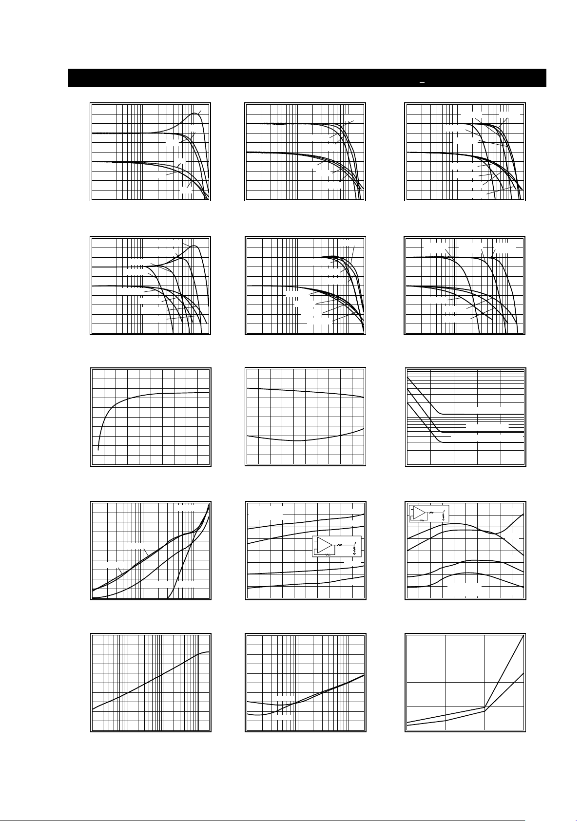
CLC407 Typical Performance Characteristics
(AV= +2, Rf= 250Ω: Vcc= + 5V, RL= 100Ω unless specified)
Frequency Response
Magnitude (1dB/div)
Phase (45
o
/div)
1
10
100
Frequency (MHz)
Gain
Phase
A
V
+2
A
V
+1
AV+1
AV-1
A
V
+2
AV -1
Frequency Response vs. R
L
Magnitude (1dB/div)
Phase (deg)
-180
-90
-135
-45
0
1
10
100
Frequency (MHz)
Gain
Phase
RL =50
RL =100
RL =1k
RL =50
RL =100
RL =1k
Frequency Response vs. V
out (Av
= +2)
Magnitude (1dB/div)
Phase (deg)
-180
-90
-135
-45
0
1
10
100
Frequency (MHz)
Gain
Phase
VO =1V
pp
VO =0.2V
pp
VO =5V
pp
VO =2V
pp
VO =5V
pp
VO =0.2V
pp
VO =1V
pp
VO =2V
pp
Frequency Response vs. V
out (Av
= +1)
Magnitude (1dB/div)
Phase (deg)
-180
-90
-135
-45
0
1
10
100
Frequency (MHz)
Gain
Phase
VO =1V
pp
VO =0.2V
pp
VO =2V
pp
VO =4V
pp
VO =2V
pp
VO =4V
pp
VO =1V
pp
VO =0.2V
pp
Frequency Response vs. V
out (Av
= -1)
Magnitude (1dB/div)
Phase (deg)
-360
-270
-315
-225
-180
1
10
100
Frequency (MHz)
Gain
Phase
VO =1V
pp
VO =0.2V
pp
VO =2V
pp
VO =4V
pp
VO =2V
pp
VO =4V
pp
VO =1V
pp
VO =0.2V
pp
Frequency Response vs. Capacitive Load
Magnitude (1dB/div)
Phase (deg)
-180
-90
-135
-45
0
1
10
100
Frequency (MHz)
Gain
Phase
CL =1kpF
Rs=10
CL =100pF
Rs= 30
CL =10pF
Rs=100
CL =1kpF
CL =100pF
CL =10pF
Maximum Output Voltage vs. R
L
Maximum Output Voltage (V
pp
)
Load (Ω)
7.0
6.0
5.0
4.0
3.0
2.0
1000200
300
400
500
Gain Flatness & Linear Phase Deviation
Magnitude (0.1dB/div)
LPD (0.5
o
/div)
0
15
30
Frequency (MHz)
Gain
Phase
Equivalent Input Noise
Noise Voltage (nV/√Hz)
Frequency (Hz)
100
10
1
1k
100
10k
100k
1M
10M
Noise Current (pA/√Hz)
100
10
1
Inverting Current = 12pA/√Hz
Voltage = 5nV/√Hz
Non-Inverting Current = 3pA/√Hz
2nd & 3rd Harmonic Distortion
Distortion (dBc)
Frequency (MHz)
-40
-50
-90
0.1
1
10
-70
-80
-60
3rd Rl = 100
2nd Rl = 1k
3rd Rl = 1k
2nd Rl = 100
Vo = 2V
pp
2nd Harmonic Distortion vs. P
out
Distortion (dBc)
Output Power (dBm)
-45
-55
-85
-10
0
10
-65
-75
500KHz
1MHz
5MHz
10MHz
10dBm = 2V
pp
0dBm = .63Vpp
+
-
50Ω
50Ω
Pout
3rd Harmonic Distortion vs. P
out
Distortion (dBc)
Output Power (dBm)
-45
-55
-85
-10
0
10
-65
-75
10dBm = 2V
pp
0dBm = .63Vpp
+
-
50Ω
50Ω
P
out
500KHz
1MHz
5MHz
10MHz
Output Resistance vs. Frequency
Output Resistance (20log Z
out
)
Frequency (MHz)
50
30
1
10
100
-10
-30
10
-50
Forward & Reverse Isolation During Disable
Gain (dB)
1
10
100
Frequency (MHz)
Forward
Reverse
-20
-40
-60
-80
-100
-120
Differential Gain & Phase
Differential Gain (%)
1
2
4
Number of 150Ω Loads
0.20
0.15
0.10
0.05
0
Differential Phase (deg)
1.00
0.75
0.50
0.25
0
Phase
Gain
3
3 http://www.national.com
Page 4

Closed Loop Gain Selection
The CLC407 is a current feedback op amp with
Rf = Rg = 250Ω on chip (in the package). Select from
three closed loop gains without using any external gain or
feedback resistors. Implement gains of +2, +1, and
-1V/V by connecting pins 2 and 3 as described in the
chart below.
The gain accuracy of the CLC407 is excellent and
stable over temperature change. The internal gain
setting resistors, Rfand Rgare diffused silicon resistors
with a process variation of ± 20% and a temperature
coefficient of ˜ 2000ppm/°C. Although their absolute
values change with processing and temperature, their
ratio (Rf/Rg) remains constant. If an external resistor is
used in series with Rg, gain accuracy over temperature
will suffer .
Non-Inverting Unity Gain Considerations (Av= +1V/V)
Achieve a gain of +1V/V by removing all resistive and
capacitive connections between pin 2 and ground plane.
Any capacitive coupling between pin 2 and ground will
cause high frequency peaking in the frequency domain
response and overshoot in the time domain response.
Minimize this capacitive coupling during layout by removing
ground plane near pins 1, 2, and 3. This minimization
should produce a response similar to the plot labeled
“open” in Graph 1. If desired flatness is greater than plot
“open” in Graph 1, two options remain to further flatten
the frequency response. First, try shorting the inverting
input (pin 2) to the non-inverting input (pin 3). This
response is labeled “short” in Graph 1. Next, try
inserting a 300Ω resistor R between the non-inverting
input (pin 2) as shown in Figure 1. This response is
labeled “300Ω ” in Graph 1. Notice an “open” produces a
response with obvious peaking and maximum bandwidth,
a “short” minimizes peaking and bandwidth, and finally
300Ω slightly extends bandwidth with minimal peaking.
Graph 1
Gain
Input Connections
Acl
Non-Inverting (pin3) Inverting (pin2)
-1V/V ground input signal
+1V/V input signal NC (open)
+2V/V input signal ground
CLC407 Typical Performance Characteristics
(AV= +2, Rf= 250Ω: Vcc= + 5V, RL= 100Ω unless specified)
IBI, IBN, VIO vs. Temperature
Offet Voltage, V
IO
(mV)
-60
-20
140
Temperature (oC)
V
IO
4.0
3.0
2.0
1.0
0
-1.0
I
BI
, I
BN
(µA)
1.0
0
-1.0
-2.0
-3.0
-4.0
20
60 100
I
BI
I
BN
CLC407 OPERATION
Small Signal Pulse Response
Output Voltage
Time (5ns/div)
0.20
0.10
-0.10
-0.20
0.00
AV-1
A
V
+2
Large Signal Pulse Response
Output Voltage
Time (5ns/div)
2.0
1.0
-1.0
-2.0
0.0
AV-1
A
V
+2
Settling Time vs. Capacitive Load
Settling Time, T
s
(ns) to 0.05% Error
10
100
1000
CL (pF)
C
L
1k
R
s
+
-
250Ω
250Ω
Vo = 2V step
T
s
R
s
CLC407
50
40
30
20
10
0
R
s
(Ω)
100
80
60
40
20
0
Short Term Settling Time
V
out
(% Final Value)
Time (ns)
0.2
0.1
-0.1
-0.2
0.0
020
100
80
6040
Vout = 2Vstep
PSRR and CMRR
PSRR/CMRR (dB)
10k
100k
1M
Frequency (Hz)
10M 100M
60
50
40
30
20
10
PSRR
CMRR
Frequency Response vs.
Unity Gain Configuration
Magnitude (1dB/div)
Frequency (MHz)
1
10
100
Short
300Ω
Open
http://www.national.com 4
Page 5

Figure 1
Enable/Disable Operation Using +5V Supplies
The CLC407 has a TTL & CMOS logic compatible
disable function. Apply a logic low (i.e. < 0.8V) to pin
8, and the CLC407 is guaranteed disabled across its
temperature range. Apply a logic high to pin 8, (i.e. >
2.0V) and the CLC407 is guaranteed enabled. Voltage,
not current, at pin 8 determines the enable/disable
state of the CLC407.
Disable the CLC407 and its inputs and output become
high impedances. While disabled, the CLC407’s quiescent power drops to 8mW.
Use the CLC407’s disable to create analog switches or
multiplexers. Implement a single analog switch with
one CLC407 positioned between an input and output.
Create an analog multiplexer with several CLC407s.
Tie the outputs together and put a different signal on
each CLC407 input.
Operate the CLC407 without connecting pin 8. An
internal 20kΩ pull-up resistor guarantees the CLC407
is enabled when pin 8 is floating.
Enable/Disable Operation for Single or
Unbalanced Supply Operation
Figure 2
Figure 2 illustrates the internal enable/disable
operation of the CLC407. When pin 8 is left floating or
is tied to +Vcc, Q1is on and pulls tail current through
the CLC407 circuitry. When pin 8 is less than 0.8V
above the supply mid-point, Q1stops tail current from
flowing in the bias circuitry. The CLC407 is now disabled.
Disable Limitations
The internal feedback resistor, Rflimits off isolation in
inverting gain configurations. Do not apply voltages
greater than +Vccor less than -Veeto pin 8.
Input - Bias Current, Impedances, and Source
Termination Considerations
The CLC407 has:
•
a 6MΩ non-inverting input impedance.
•
100nA non-inverting input bias current.
If a large source impedance application is considered,
remove all parasitic capacitance around the non-inverting input and source traces. Parasitic capacitances
near the input and source act as a low-pass filter and
reduce bandwidth.
Current feedback op amps have uncorrelated input
bias currents. These uncorrelated bias currents
prevent source impedance matching on each input
from cancelling offsets. Refer to application note
OA-07 of the data book to find specific circuits to
correct DC offsets.
Layout Considerations
Whenever questions about layout arise, USE THE
EV ALUATION BOARD AS ATEMPLA TE.
Use the 730013 and 730026 evaluation boards for the
DIP and SOIC respectively. These board layouts were
optimized to produce the typical performance of the
CLC407 shown in the data sheet. To reduce parasitic
capacitances, the ground plane was removed near
pins 2, 3, and 6. To reduce series inductance, trace
lengths of components and nodes were minimized.
Parasitics on traces degrade performance. Minimize
coupling from traces to both power and ground
planes. Use low inductance resistors for leaded
components .
Do not use dip sockets for the CLC407 DIP amplifiers.
These sockets can peak the frequency domain
response or create overshoot in the time domain
response. Use flush-mount socket pins if socketing
cannot be avoided. The 730013 circuit board device
holes are sized for Cambion P/N 450-2598 socket pins
or their functional equivalent.
Insert the back matching resistor R
out
shown in
Figure 3 when driving coaxial cable or a capacitive
load. Use the plot in the typical performance section
labeled “Settling Time vs. Capacitive Load” to determine
the optimum resistor value for R
out
for different capacitive loads. This optimal resistance improves settling
time for pulse-type applications and increases stability.
Figure 3
SMA
Output
SMA
Input
R
in
50Ω
R
out
50Ω
+5V
-5V
+
+
C
1
0.1µfd
C
2
0.1µfd
C
3
6.8µfd
C
4
6.8µfd
J1 = 0Ω
1
CLC407
7
6
8
5
3
4
2
20kΩ
20kΩ
Pin 8
Disable
Q2Q
1
Pin 4
-V
ee
20kΩ
Bias
Circuitry
I Tail
Supply
Mid-Point
Pull-up
Resistor
Pin 7
+V
cc
CLC407
NOTE: Pins 4, 7, 8 are external
V
cc -Vee
2
SMA
Output
SMA
Input
R
in
50Ω
R
out
50Ω
R
1
CLC407
7
6
8
5
3
4
2
5 http://www.national.com
Page 6

Use power-supply bypassing capacitors when
operating this amplifier. Choose quality 0.1µF ceramics
for C1and C2. Choose quality 6.8µF tantalum capacitors
for C3and C4. Place the 0.1µF capacitors within 0.1
inches from the power pins. Place the 6.8µF capacitors
within 3/4 inches from the power pins.
Special Evaluation Board
Considerations for the CLC407
To optimize off-isolation of the CLC407, cut the Rftrace on
both the 730013 and the 730027 evaluation boards. This
cut minimizes capacitive feedthrough between the input
and the output. Figure 4 shows where to cut both evaluation boards for improved off-isolation.
Figure 4
Video Performance vs. I
EX
Improve the video performance of the CLC407 by drawing
extra current from the amplifier’s output stage. Using a
single external resistor as shown in Figure 5, you can
adjust the differential phase. Video performance vs. IEXis
illustrated below in Graph 2. This graph represents
positive video performance with negative synchronization
pulses.
Graph 2
The value for Rpd in Figure 5 is determined by:
at +5V supplies.
Figure 5
Video Cable Driver
The CLC407 was designed to produce exceptional video
performance at all three closed-loop gains. At the noninverting gain of 2V/V configuration, back terminate the
cable using R
out
. A typical cable driving configuration is
shown below in Figure 6.
Figure 6
N:1 Mux Cable Driver
The CLC407 is capable of multiplexing several signals on a
single analog output bus. The front page shows how a 2:1
multiplexer is implemented. An N:1 multiplexer is implement ed in an analogous fashion by using an N:1 decoder to
enable/disable the appropriate number of CLC407’s.
Ordering Information
Model Temperature Range Description
CLC407AJP -40
˚
C to +85˚C 8-pin PDIP
CLC407AJE -40
˚
C to +85˚C 8-pin SOIC
CLC407AIB -40
˚
C to +85˚C 8-pin CerDIP
CLC407ALC -40
˚
C to +85˚C dice
CLC407A8B -55
˚
C to +125˚C 8-pin CerDIP, MIL-STD-883
CLC407AMC -55
˚
C to +125˚C dice, MIL-STD-883
Contact factory for other packages and DESC SMD number.
Package Thermal Resistance
Package
q
jc
q
jA
Plastic (AJP) 75
˚
/W 125˚/W
Surface Mount (AJE) 130
˚
/W 150˚/W
CerDip 65
˚
/W 155˚/W
730013
REV C
Cut trace here
SMA
Output
SMA
Input
R
in
50Ω
R
out
50Ω
+5V
-5V
+
+
C
1
0.1µfd
C
2
0.1µfd
C
3
6.8µfd
C
4
6.8µfd
J1 = 0Ω
1
CLC407
7
6
8
5
3
4
2
R
pd
I
EX
Differential Gain & Phase vs. I
EX
Differential Gain (%)
IEX in mA
0.25
0.20
0.15
0.10
0.05
0
204
6
8
10
Differential Phase (deg)
0.25
0.20
0.15
0.10
0.05
0
Phase
Gain
12
14
16
18
R
5
I
pd
EX
=
Coax
50Ω
SMA
Input
R
in
50Ω
R
out
50Ω
+5V
-5V
+
+
C
1
0.1µfd
C
2
0.1µfd
C
3
6.8µfd
C
4
6.8µfd
J1 = 0Ω
1
CLC407
7
6
8
5
3
4
2
50Ω
Video
Output
R6R3R1
R7
R8
R5
C3
R2
R4
C4
ROUT
OUT
C6C2C1
C5
C8
IN
RIN
RG
RF
C7
-Vcc+V
cc
GND
Comlinear
A National Semiconductor Company
(303) 226-0500
+
+
Cut trace here
http://www.national.com 6
Page 7

This page intentionally left blank.
7 http://www.national.com
Page 8

Comlinear CLC407
Low-Cost, Low-Power, Programmable Gain Buffer with Disable
http://www.national.com 8 Lit #150207-003
Customer Design Applications Support
National Semiconductor is committed to design excellence. For sales, literature and technical support, call the
National Semiconductor Customer Response Group at 1-800-272-9959 or fax 1-800-737-7018.
Life Support Policy
National’s products are not authorized for use as critical components in life support devices or systems without the express written approval
of the president of National Semiconductor Corporation. As used herein:
1. Life support devices or systems are devices or systems which, a) are intended for surgical implant into the body, or b) support or
sustain life, and whose failure to perform, when properly used in accordance with instructions for use provided in the labeling, can
be reasonably expected to result in a significant injury to the user.
2. Acritical component is any component of a life support device or system whose failure to perform can be reasonably expected to
cause the failure of the life support device or system, or to affect its safety or effectiveness.
National Semiconductor National Semiconductor National Semiconductor National Semiconductor
Corporation Europe Hong Kong Ltd. Japan Ltd.
1111 West Bardin Road Fax: (+49) 0-180-530 85 86 13th Floor, Straight Block Tel: 81-043-299-2309
Arlington, TX 76017 E-mail: europe.support.nsc.com Ocean Centre, 5 Canton Road Fax: 81-043-299-2408
Tel: 1(800) 272-9959 Deutsch Tel: (+49) 0-180-530 85 85 Tsimshatsui, Kowloon
Fax: 1(800) 737-7018 English Tel: (+49) 0-180-532 78 32 Hong Kong
Francais Tel: (+49) 0-180-532 93 58 Tel: (852) 2737-1600
Italiano Tel: (+49) 0-180-534 16 80 Fax: (852) 2736-9960
National does not assume any responsibility for use of any circuitry described, no circuit patent licenses are implied and National reserves the right at any time without notice to change said
circuitry and specifications.
N
 Loading...