

Page 1
Frequency Response (Av = +2V/V)
Features
■
Low-cost
■
Very low input bias current: 100nA
■
High input impedance: 6MΩ
■
110MHz -3dB bandwidth (Av= +2)
■
Low power: Icc= 3.5mA
■
Ultra-fast enable/disable times
■
High output current: 60mA
Applications
■
Desktop video systems
■
Multiplexers
■
Video distribution
■
Flash A/D driver
■
High-speed switch/driver
■
High-source impedance applications
■
Peak detector circuits
■
Professional video processing
■
High resolution monitors
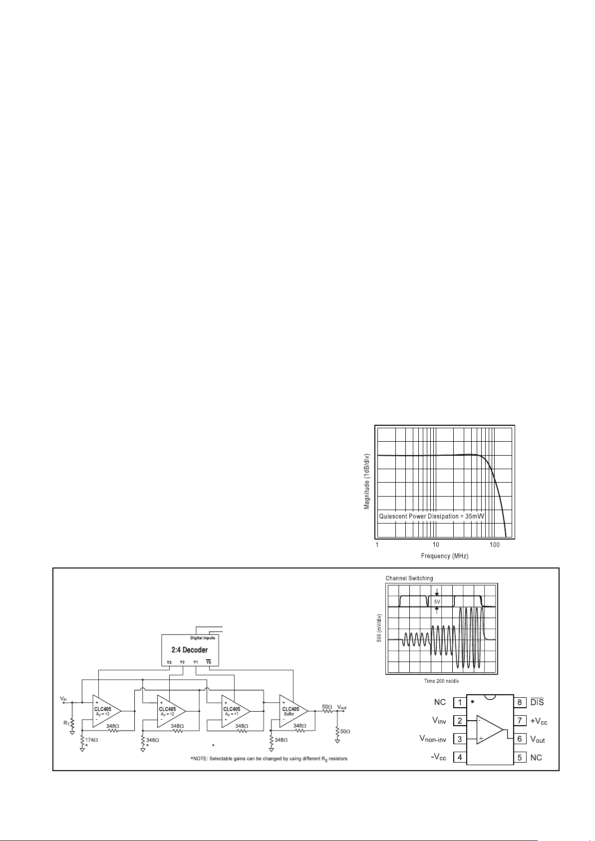
Typical Application
Wideband Digitally Controlled
Programmable Gain Amplifier
Pinout
DIP & SOIC
General Description
The CLC405 is a low-cost, wideband (110MHz) op amp featuring a TTL-compatible disable which quickly switches off in 18ns
and back on in 40ns. While disabled, the CLC405 has a very high
input/output impedance and its total power consumption drops to
a mere 8mW.When enabled, the CLC405 consumes only 35mW
and can source or sink an output current of 60mA. These
features make the CLC405 a versatile, high-speed solution for
demanding applications that are sensitive to both power and cost.
Utilizing National’s proven architectures, this current feedback
amplifier surpasses the performance of alternative solutions and
sets new standards for low power at a low price. This powerconserving op amp achieves low distortion with -72dBc and
-70dBc for second and third harmonics respectively. Many high
source impedance applications will benefit from the CLC405’s
6MΩ input impedance. And finally, designers will have a bipolar
part with an exceptionally low 100nA non-inverting bias current.
With 0.1dB flatness to 50MHz and low differential gain and phase
errors, the CLC405 is an ideal part for professional video
processing and distribution. However, the 110MHz -3dB bandwidth (Av= +2) coupled with a 350V/µs slew rate also make the
CLC405 a perfect choice in cost-sensitive applications such as
video monitors, fax machines, copiers, and CATV systems.
CLC405
Low-Cost, Low-Power, 110MHz Op Amp with Disable
N
June 1999
CLC405
Low-Cost, Low-Power, 110MHz Op Amp with Disable
© 1999 National Semiconductor Corporation http://www.national.com
Printed in the U.S.A.
Page 2
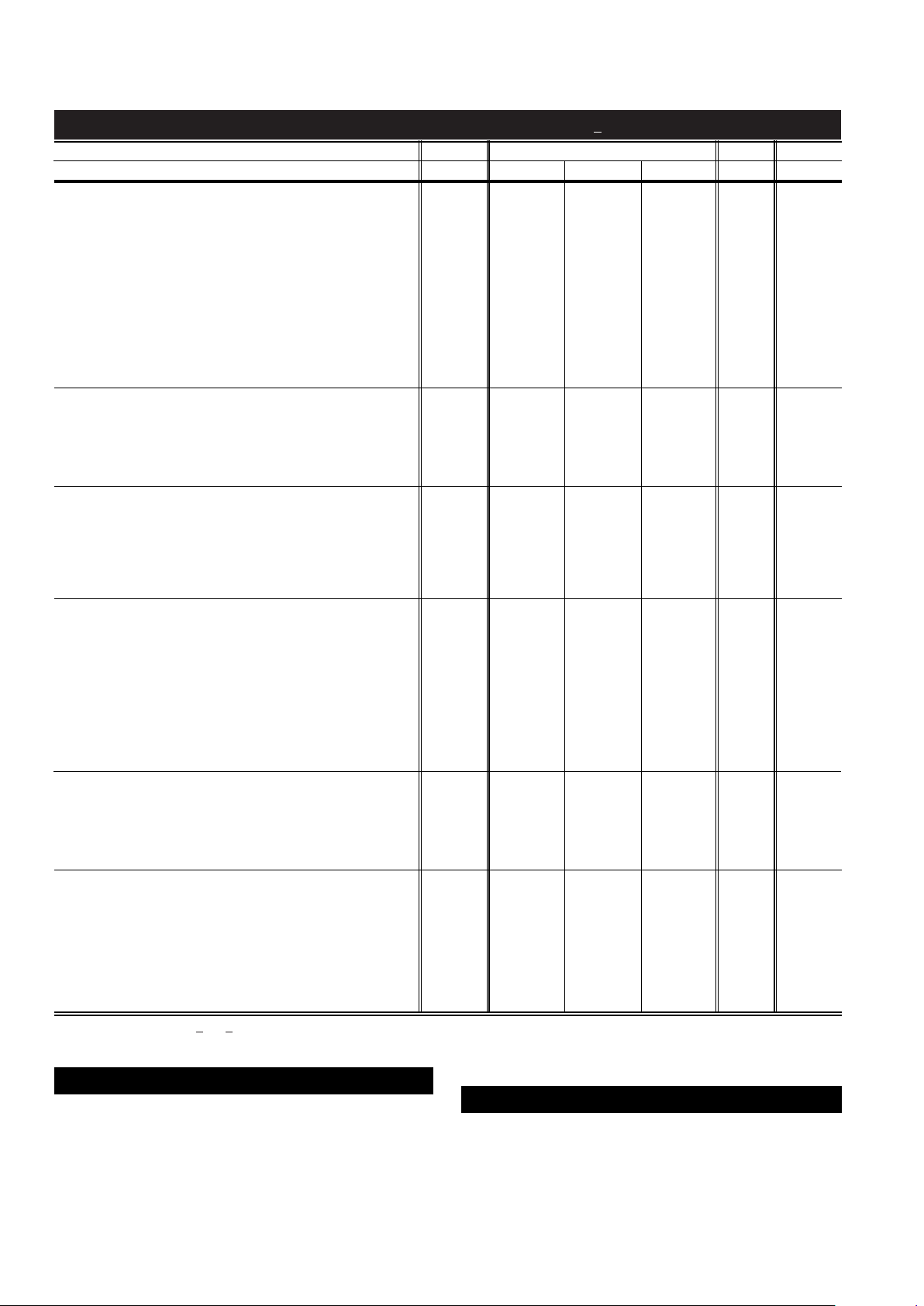
PARAMETERS CONDITIONS TYP MIN/MAX RATINGS UNITS NOTES
Ambient T emper ature CLC405AJ +25˚C +25˚C 0 to 70˚C -40 to 85˚C
FREQUENCY DOMAIN RESPONSE
-3dB bandwidth V
out
< 1.0V
pp
110 75 50 45 MHz
V
out
< 5.0V
pp
42 31 27 26 MHz 1
-3dB bandwidth A
V
= +1 V
out
< 0.5Vpp(Rf= 2K) 135 MHz
±
0.1dB bandwidth V
out
< 1.0V
pp
50 15 MHz
gain flatness V
out
< 1.0V
pp
peaking DC to 200MHz 0 0.6 0.8 1.0 dB
rolloff <30MHz 0.05 0.3 0.4 0.5 dB
linear phase deviation <20MHz 0.3 0.6 0.7 0.7 deg
differential gain NTSC, R
L
=150Ω 0.01 0.03 0.04 0.05 %
NTSC, R
L
=150Ω (Not e 2 ) 0.01 % 2
differential phase NTSC, R
L
=150Ω 0.25 0.4 0.5 0.55 deg
NTSC, R
L
=150Ω (Not e 2 ) 0.08 deg 2
TIME DOMAIN RESPONSE
rise and fall time 2V step 5 7.5 8.2 8.4 ns
settling time to 0.05% 2V step 18 27 36 39 ns
overshoot 2V step 3 12 12 12 %
slew rate A
V
= +2 2V step 350 260 225 215 V/µs
A
V
= -1 1V step 650 V/µs
DISTORTION AND NOISE RESPONSE
2
nd
harmonic distortion 2Vpp, 1MHz/10MHz -72/-52 -46 -45 -44 dBc B
3
rd
harmonic distortion 2Vpp, 1MHz/10MHz -70/-57 -50 -47 -46 dBc B
equivalent input noise
non-inverting voltage >1MHz 5 6.3 6.6 6.7 nV/√Hz
inverting current >1MHz 12 15 16 17 pA/√Hz
non-inverting current >1MHz 3 3.8 4 4.2 pA/√Hz
STATIC DC PERFORMANCE
input offset voltage 1 5 7 8 mV A
average drift 30 50 50 µV/˚C
input bias current non-inverting 100 900 1600 2800 nA A
average drift 3 8 11 nA/˚C
input bias current inverting 1 5 7 10 µAA
average drift 17 40 45 nA/˚C
power supply rejection ratio DC 52 47 46 45 dB
common-mode rejection ratio DC 50 45 44 43 dB
supply current R
L
= ∞ 3.5 4.0 4.1 4.4 mA A
disabled R
L
= ∞ 0.8 0.9 0.95 1 mA A
SWITCHING PERFORMANCE
turn on time 40 55 58 58 ns
turn off time to >50dB attn. @ 10MHz 18 26 30 32 ns
off isolation 10MHz 59 55 55 55 dB
high input voltage V
IH
222V
low input voltage V
IL
0.8 0.8 0.8 V
MISCELLANEOUS PERFORMANCE
input resistance non-inverting 6 3 2.4 1 MΩ
input resistance inverting 182 Ω
input capacitance non-inverting 1 2 2 2 pF
common mode input range
±
2.2 1.8 1.7 1.5 V
output voltage range R
L
= 100Ω + 3.5,-2.8 +3.1,-2.7 +2.9,-2.6 +2.4,-1.6 V
output voltage range R
L
= ∞ +4.0,-3.3 +3.9,-3.2 +3.8,-3.1 +3.7,-2.8 V
output current 40 40 38 20 mA
output resistance, closed loop 0.06 0.2 0.25 0.4 Ω
Recommended gain range +1 to +40V/V
Min/max ratings are based on product characterization and simulation. Individual parameters are tested as noted. Outgoing quality levels are
determined from tested parameters.
CLC405 Electrical Characteristics
(AV= +2, Rf= 348Ω:Vcc= + 5V, RL= 100Ω unless specified)
Absolute Maximum Ratings
supply voltage
±
7V
I
out
is short circuit protected to ground
common-mode input voltage
±
Vcc
maximum junction temperature +150˚C
storage temperature range -65˚C to +150˚C
lead temperature (soldering 10 sec) +300˚C
Notes
1) At temps < 0˚C, spec is guaranteed for RL= 500Ω.
2) An 825Ω pull-down resistor is connected between
V
o
and -Vcc.
A) J-level:spec is 100% tested at +25˚C
B)Guaranteed at 10MHz.
http://www.national.com 2
Transitor count 68
Page 3

CLC405 Typical Performance Characteristics
(AV= +2, Rf= 348Ω:Vcc= + 5V,RL= 100Ω unless specified)
Non-Inverting Frequency Response
Magnitude (1dB/div)
Phase (deg)
-180
-90
-135
-45
0
1
10
100
Frequency (MHz)
Gain
Phase
A
V
+4
A
V
+2
AV+2
Rf =348
AV+1
Rf =2k
AV+10
Rf =100
AV+4
Rf =200
AV+10
AV+1
Inverting Frequency Response
Magnitude (1dB/div)
Phase (deg)
-360
-270
-315
-225
-180
1
10
100
Frequency (MHz)
Gain
Phase
A
V
-4
A
V
-2
AV-4
Rf =200
AV-1
Rf =348
AV-10
Rf =500
AV-10
AV-1
AV-2
Rf =200
Frequency Response For Various RLs
Magnitude (1dB/div)
Phase (deg)
-180
-90
-135
-45
0
1
10
100
Frequency (MHz)
Gain
Phase
RL=50
RL=1k
RL=100
RL=100
RL=50
RL=1k
Frequency Response vs. V
out
Magnitude (1dB/div)
Phase (deg)
-180
-90
-135
-45
0
1
10
100
Frequency (MHz)
Gain
Phase
Vo=2V
pp
Vo=5V
pp
Vo=0.2V
pp
Vo=2V
pp
Vo=1V
pp
Vo=5V
pp
Vo=0.2V
pp
Vo=1V
pp
Frequency Response vs. Capacitive Load
Magnitude (1dB/div)
1
10
100
Frequency (MHz
)
CL= .001µfd
Rs =10
CL=100pF
Rs =30
CL=10pF
Rs =100
C
L
1k
R
s
+
-
348Ω
348Ω
Gain Flatness & Linear Phase Deviation
Magnitude (0.1dB/div)
Frequency (MHz
)
Phase
Gain
LPD (0.5
o
/div)
03015
Maximum Output Voltage vs. R
L
Maximum Output Voltage (V
pp
)
Load (Ω)
7.0
6.0
5.0
4.0
3.0
2.0
1000200
300
400
500
Open Loop Transimpedance Gain, Z(s)
20 log [|V
o
/|
i
/1Ω]
1k
10M
100M
Frequency (Hz)
130
110
90
70
50
30
Phase (deg)
200
160
120
80
40
0
Gain
Phase
1M
100k
10k
100Ω
-
+
CLC405
V
o
I
i
Equivalent Input Noise
Noise Voltage (nV/√Hz)
Frequency (Hz)
100
10
1
1k
100
10k
100k
1M
10M
Noise Current (pA/√Hz)
100
10
1
Inverting Current = 12pA/√Hz
Voltage = 5nV/√Hz
Non-Inverting Current = 3pA/√Hz
2nd & 3rd Harmonic Distortion
Distortion (dBc)
Frequency (MHz)
-40
-50
-90
0.1
1
10
-70
-80
-60
3rd Rl = 100
2nd Rl = 1k
3rd Rl = 1k
2nd Rl = 100
Vo = 2V
pp
2nd Harmonic Distortion vs. P
out
Distortion (dBc)
Output Power (dBm)
-45
-55
-85
-10
0
10
-65
-75
500KHz
1MHz
5MHz
10MHz
10dBm = 2V
pp
0dBm = .63Vpp
+
-
50Ω
50Ω
Pout
3rd Harmonic Distortion vs. P
out
Distortion (dBc)
Output Power (dBm)
-45
-55
-85
-10
0
10
-65
-75
10dBm = 2V
pp
0dBm = .63Vpp
+
-
50Ω
50Ω
P
out
500KHz
1MHz
5MHz
10MHz
Output Resistance vs. Frequency
Output Resistance (20log Z
out
)
Frequency (MHz)
50
30
1
10
100
-10
-30
10
-50
Forward and Reverse Gain During Disable
Gain (dB)
Frequency (MHz)
0
-20
1
10
100
-60
-80
-40
-100
Forward
Reverse
Differential Gain and Phase
Differential Gain (%)
Differential Phase (deg)
Number of 150Ω Loads
0.20
0.15
1
2
3
0.05
0
0.10
Gain
Phase
4
1.00
0.75
0.25
0
0.50
75Ω
+
-
348Ω
348Ω
75Ω
CLC405
825Ω
75Ω
V
out
V
in
-V
cc
f = 3.58MHz
3 http://www.national.com
Page 4

CLC405 Typical Performance Characteristics
(AV= +2, Rf= 348Ω:Vcc= + 5V,RL= 100Ω unless specified)
IBI, IBN, VIO vs. Temperature
Offet Voltage, V
IO
(mV)
-60
-20
140
Temperature (oC)
V
IO
4.0
3.0
2.0
1.0
0
-1.0
I
BI
, I
BN
(µA)
1.0
0
-1.0
-2.0
-3.0
-4.0
20
60 100
I
BI
I
BN
CLC405 OPERATION
Feedback Resistor
The feedback resistor, Rf, determines the loop gain and
frequency response for a current feedback amplifier.
Unless otherwise stated, the performance plots and data
sheet specify CLC405 operation with Rfof 348Ω at a
gain of +2V/V. Optimize frequency response for different
gains by changing Rf. Decrease Rfto peak frequency
response and extend bandwidth. Increase Rfto roll off
of the frequency response and decrease bandwidth. Use
a 2kΩ Rffor unity gain, voltage follower circuits.
Use application note OA-13 to optimize your Rfselection. The equations in this note are a good starting
point for selecting Rf. The value for the inverting input
impedance for OA-13 is approximately 182Ω.
Enable/Disable Operation Using ±5V Supplies
The CLC405 has a TTL & CMOS logic compatible
disable function. Apply a logic low (i.e. < 0.8V) to pin
8, and the CLC405 is guaranteed disabled across its
temperature range. Apply a logic high to pin 8, (i.e. >
2.0V) and the CLC405 is guaranteed enabled. V oltage,
not current, at pin 8 determines the enable/disable
state of the CLC405.
Disable the CLC405 and its inputs and output become
high impedances. While disabled, the CLC405’s
quiescent power drops to 8mW.
Use the CLC405’s disable to create analog switches or
multiplex ers.Implement a single analog switch with one
CLC405 positioned between an input and output.
Create an analog multiplexer with several CLC405s.
Tie the outputs together and put a different signal on
each CLC405 input.
Operate the CLC405 without connecting pin 8. An
internal 20kΩ pull-up resistor guarantees the CLC405
is enabled when pin 8 is floating.
Enable/Disable Operation for Single or
Unbalanced Supply Operation
Figure 1
Figure 1 illustrates the internal enable/disable operation of the CLC405. When pin 8 is left floating or is tied
to +V
cc
, Q1 is on and pulls tail current through the
CLC405 bias circuitry. When pin 8 is less than
0.8V above the supply midpoint, Q1 stops tail current
from flowing in the CLC405 circuitry. The CLC405 is
now disabled.
Disable Limitations
The feedback resistor, Rf, limits off isolation in inverting
gain configurations. Do not apply voltages greater than
+Vccor less than -Veeto pin 8 or any other pin.
Small Signal Pulse Response
Output Voltage
Time (5ns/div)
0.20
0.10
-0.10
-0.20
0.00
AV-1
A
V
+1
Large Signal Pulse Response
Output Voltage
Time (5ns/div)
2.0
1.0
-1.0
-2.0
0.0
AV-2
A
V
+2
Settling Time vs. Capacitive Load
Settling Time, T
s
(ns) to 0.05% Error
10
100
1000
CL (pF)
C
L
1k
R
s
+
-
348Ω
348Ω
Vo = 2V step
T
s
R
s
CLC405
50
40
30
20
10
0
R
s
(Ω)
100
80
60
40
20
0
Short Term Settling Time
V
out
(% Final Value)
Time (ns
)
0.2
0.1
-0.1
-0.2
0.0
020
100
80
6040
Vout = 2Vstep
PSRR and CMRR
PSRR/CMRR (dB)
10k
100k
1M
Frequency (Hz
)
10M 100M
60
50
40
30
20
10
PSRR
CMRR
20kΩ
20kΩ
Pin 8
Disable
Q2Q
1
Pin 4
-V
ee
20kΩ
Bias
Circuitry
I Tail
Supply
Mid-Point
Pull-up
Resistor
Pin 7
+V
cc
CLC405
NOTE: Pins 4, 7, 8 are external
V
cc -Vee
2
http://www.national.com 4
Page 5

Input - Bias Current, Impedances, and Source
Termination Considerations
The CLC405 has:
•
a 6MΩ non-inverting input impedance.
•
a 100nA non-inverting input bias current.
If a large source impedance application is considered,
remove all parasitic capacitance around the non-in v erting input and source traces. Parasitic capacitances
near the input and source act as a low-pass filter and
reduce bandwidth.
Current feedback op amps have uncorrelated input
bias currents.These uncorrelated bias currents prevent
source impedance matching on each input from canceling offsets. Refer to application note OA-07 of the
data book to find specific circuits to correct DC offsets.
Layout Considerations
Whenever questions about layout arise, USE THE
EVALUATION BOARD AS A TEMPLATE.
Use the CLC730013 and CLC730027 evaluation
boards for the DIP and SOIC respectively. These board
layouts were optimized to produce the typical performance of the CLC405 shown in the data sheet. To
reduce parasitic capacitances, the ground plane was
removed near pins 2, 3, and 6. To reduce series inductance, trace lengths of components and nodes were
minimized.
Parasitics on traces degrade performance. Minimize
coupling from traces to both power and ground planes.
Use low inductive resistors for leaded components.
Do not use dip sockets for the CLC405 DIP amplifiers.
These sockets can peak the frequency domain
response or create overshoot in the time domain
response. Use flush-mount socket pins when socketing is necessary. The 730013 circuit board device
holes are sized for Cambion P/N 450-2598 socket pins
or their functional equivalent.
Insert the back matching resistor (R
out)
shown in Figure
2 when driving coaxial cable or a capacitive load. Use
the plot in the typical performance section labeled
“Settling Time vs. Capacitive Load” to determine the
optimum resistor value for R
out
for different capacitive
loads.This optimal resistance improves settling tim for
pulse-type applications and increases stability.
Figure 2
Use power-supply bypassing capacitors when operating this amplifier. Choose quality 0.1µF ceramics for C
1
and C2. Choose quality 6.8µF tantalum capacitors for
C3and C4. Place the 0.1µF capacitors within 0.1 inches from the power pins. Place the 6.8µF capacitors
within 3/4 inches from the power pins.
Video Performance vs . I
EX
Improve the video performance of the CLC405 by
drawing extra current from the amplifier output stage.
Using a single external resistor as shown in Figure 3,
you can adjust the differential phase. Video performance vs.IEXis illustrated below in Graph 1. This graph
represents positive video performance with negative
synchronization pulses.
Graph1
Figure 3
The value for Rpdin Figure 3 is determined by :
at +5V supplies.
Wideband Digital PGA
As shown on the front page, the CLC405 is easily configured as a digitally controlled programmable gain
amplifier. Make a PGA by configuring several amplifiers
at required gains. Keep Rfnear 348Ω and change R
g
for each different gain. Use a TTL decoder that has
enough outputs to control the selection of different gains
and the buffer stage. Connect the buffer stage like the
buffer of the front page. The buffer isolates each gain
stage from the load and can produce a gain of zero for
a gain selection of zero. Use of an inverter (7404) on the
buffer disable pin to keep the buffer operational at all
gains except zero. Or float the buffer disable pin for a
continuous enable state.
Differential Gain & Phase vs. I
EX
Differential Gain (%)
IEX in mA
0.25
0.20
0.15
0.10
0.05
0
204
6
8
10
Differential Phase (deg)
0.25
0.20
0.15
0.10
0.05
0
Phase
Gain
12
14
16
18
SMA
Output
SMA
Input
R
in
50Ω
R
f
348Ω
R
out
50Ω
3
7
6
4
2
+5V
-5V
+
+
+
-
R
g
348Ω
C
1
0.1µfd
C
2
0.1µfd
C
3
6.8µfd
C
4
6.8µfd
CLC405
R
pull
down
R
f
R
out
+
-
CLC405
R
g
V
in
-V
cc
R
t
V
out
Extra I
-5V
+5V
R
5
I
pd
EX
=
5 http://www.national.com
Page 6

Amplitude Equalization
Sending signals over coaxial cable greater than 50
meters in length will attenuate high frequency signal
components. Equalizers restore the attenuated components of this signal. The circuit in Figure 4, is an op
amp equalizer.The RC networks peak the response of
the CLC405 at higher frequencies. This peaking
restores cable-attenuated frequencies. Graph 2 shows
how the equalizer actually restored a digital word
through 150 meters of coaxial cable.
Figure 4
Graph 2
Amplitude Equalizer
Place the first zero (fz1) at some low frequency (540
khz for Graph 2). R1& C1produce a pole (fp1@
750khz) that cancels fz1. Place a second zero at a
higher frequency (fz2@ 12Mhz). R2& C2provide a
canceling pole (of fp2= 25Mhz).
Graph 3 shows the closed loop response of the op
amp equalizer with equations for the poles, zeros,
and gains.
Graph 3
Note: For very-high frequency equalization, use a higher
bandwidth part (i.e. CLC44X)
Ordering Information
Model Temperature Range Description
CLC405AJP -40˚C to +85˚C 8-pin PDIP
CLC405AJE -40˚C to +85˚C 8-pin SOIC
CLC405AIB -40˚C to +85˚C 8-pin CerDIP
CLC405ALC -40˚C to +85˚C dice
CLC405AMC -55˚C to +125˚C dice, MIL-STD-883
CLC405A8B -55˚C to +125˚C 8-pin CerDIP, MIL-STD-883
Contact factory for other packages and DESC SMD number.
Pac kage Thermal Resistance
Package
θθ
jc
θθ
jA
Plastic (AJP) 75˚/W 125˚/W
Surface Mount (AJE) 130˚/W 150˚/W
CerDip 65˚/W 155˚/W
Rf = 348Ω
+
-
CLC405
R
g
Input
R
t
Output
C
1
R
1
C
2
R
2
RC Networks
Coaxial Cable
Digital Word Amplitude Equalization
Amplitude (0.5V/div)
Time (200ns/div)
Unequalized
Equalized
Closed Loop Equalizer Frequency Response
Log Magnitude
Frequency (Hz)
fz
1
2R C R C
1
11g1
=
+
()
π
fp
1
2RC
1
11
=
π
fz
1
2R C R C
2
22eq2
=
+
()
π
fp
1
2RC
2
22
=
π
R R llR
eq1g
=
fz
1
fp
1
fz
2
fp
1
G
1
G
2
G 20log (1
R
2R
)
1
g
1
=+
G 20log (1
R
2R
)
2
eq
2
=+
The values used to produce Graph 2 are:
Rg= 348Ω C1= 470pF C2= 70pF
R1= 450Ω R2= 90Ω
http://www.national.com 6
CLC405
Low-Cost, Low-Power, 110MHz Op Amp with Disable
Customer Design Applications Support
National Semiconductor is committed to design excellence. For sales, literature and technical support, call the
National Semiconductor Customer Response Group at 1-800-272-9959 or fax 1-800-737-7018.
Life Support Policy
National’s products are not authorized for use as critical components in life support devices or systems without the express written approval of
the president of National Semiconductor Corporation. As used herein:
1. Life support devices or systems are devices or systems which, a) are intended for surgical implant into the body, or b) support or
sustain life, and whose failure to perform, when properly used in accordance with instructions for use provided in the labeling, can
be reasonably expected to result in a significant injury to the user.
2. A critical component is any component of a life support device or system whose failure to perform can be reasonably expected to
cause the failure of the life support device or system, or to affect its safety or effectiveness.
National Semiconductor National Semiconductor National Semiconductor National Semiconductor
Corporation Europe Hong Kong Ltd. Japan Ltd.
1111 West Bardin Road Fax: (+49) 0-180-530 85 86 2501 Miramar Tower Tel: 81-043-299-2309
Arlington, TX 76017 E-mail: europe.support.nsc.com 1-23 Kimberley Road Fax: 81-043-299-2408
Tel: 1(800) 272-9959 Deutsch Tel: (+49) 0-180-530 85 85 Tsimshatsui, Kowloon
Fax:1(800) 737-7018 English Tel: (+49) 0-180-532 78 32 Hong Kong
Francais Tel: (+49) 0-180-532 93 58 Tel:(852) 2737-1600
Italiano Tel: (+49) 0-180-534 16 80 Fax:(852) 2736-9960
National does not assume any responsibility for use of any circuitry described, no circuit patent licenses are implied and National reserves the right at any time without notice to change said
circuitry and specifications.
N
 Loading...