

Page 1
CLC404
Wideband, High Slew Rate, Monolithic Op Amp
General Description
The CLC404 is a high speed, monolithic op amp that combines low power consumption (110mW typical, 120mW
maximum) with superior large signal performance. Operating
off of
±
5V supplies, the CLC404 demonstrates a large signal
bandwidth (5V
PP
output) of 165MHz. The bandwidth performance, along with other speed characteristics such as rise
and fall time (2.1ns for a 5V step), is nearly identical to the
small signal performance since slew rate is not limiting factor
in the CLC404 design.
With its 175MHz bandwidth and 10ns settling (0.2%), the
CLC404 is ideal for driving ultra fast flash A/D converters.
The 0.5˚ deviation from linear phase, coupled with -53dBc
2nd harmonic distortion and -60dBc 3rd harmonic distortion
(both at 20MHz), is well suited for many digital and analog
communication applications. These same characteristics,
along with 70mA output current, differential gain of 0.07%,
and differential phase at 0.03˚, make the CLC404 an appropriate high performance solution for video distribution and
line driving applications.
Constructed using an advanced, complementary bipolar process and proven current feedback topologies, the CLC404
provides performance far beyond that of other monolithic op
amps. The CLC404 is available in several versions to meet a
variety of requirements.
Enhanced Solutions (Military/Aerospace)
SMD Number: 5962-90994
Space level versions also available.
For more information, visit http://www.national.com/mil
Features
n 165MHz large signal bandwidth (5VPP)
n 2600V/µs slew rate
n Low Power: 110mW
n Low distortion: −53dBc at 20MHz
n 10ns settling to 0.2%
n 0.07% diff. gain, 0.03˚ diff. phase
Applications
n Fast A/D conversion
n Line drivers
n Video distribution
n High speed communications
n Radar, IF processors
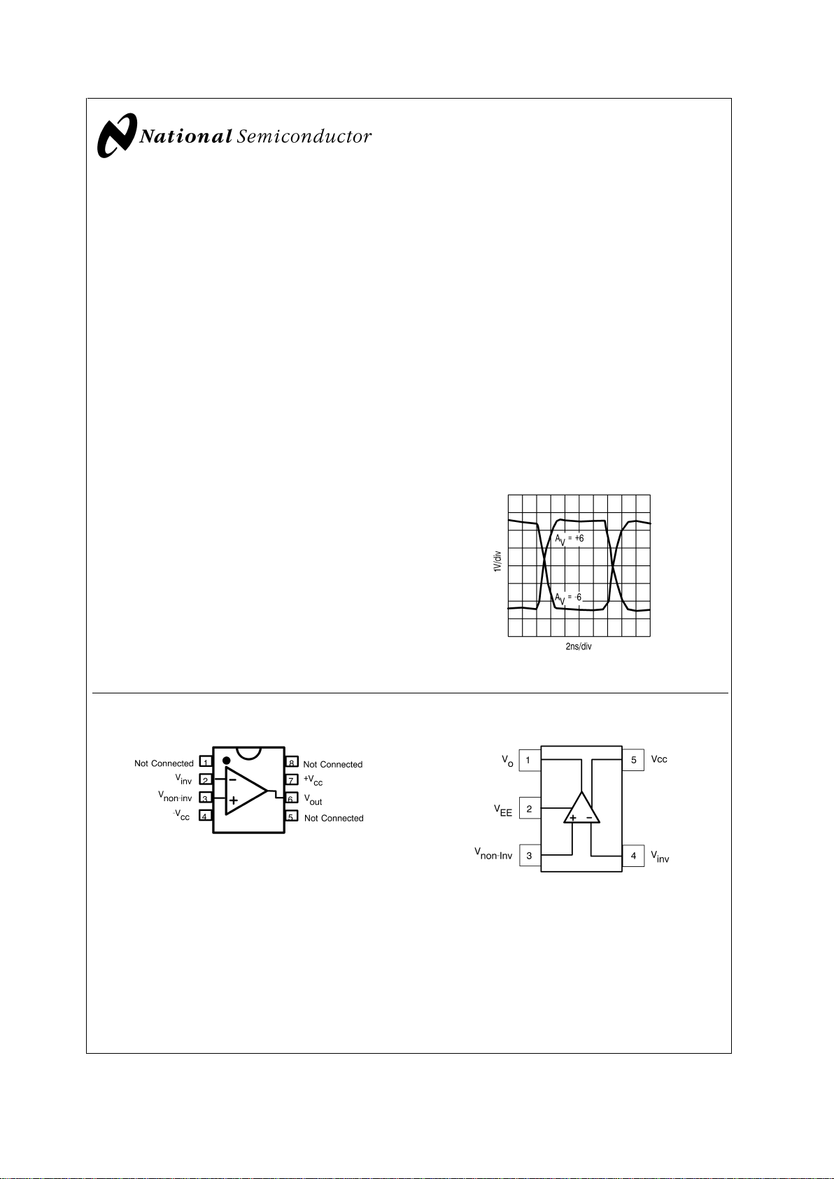
Large Signal Pulse Response
01274607
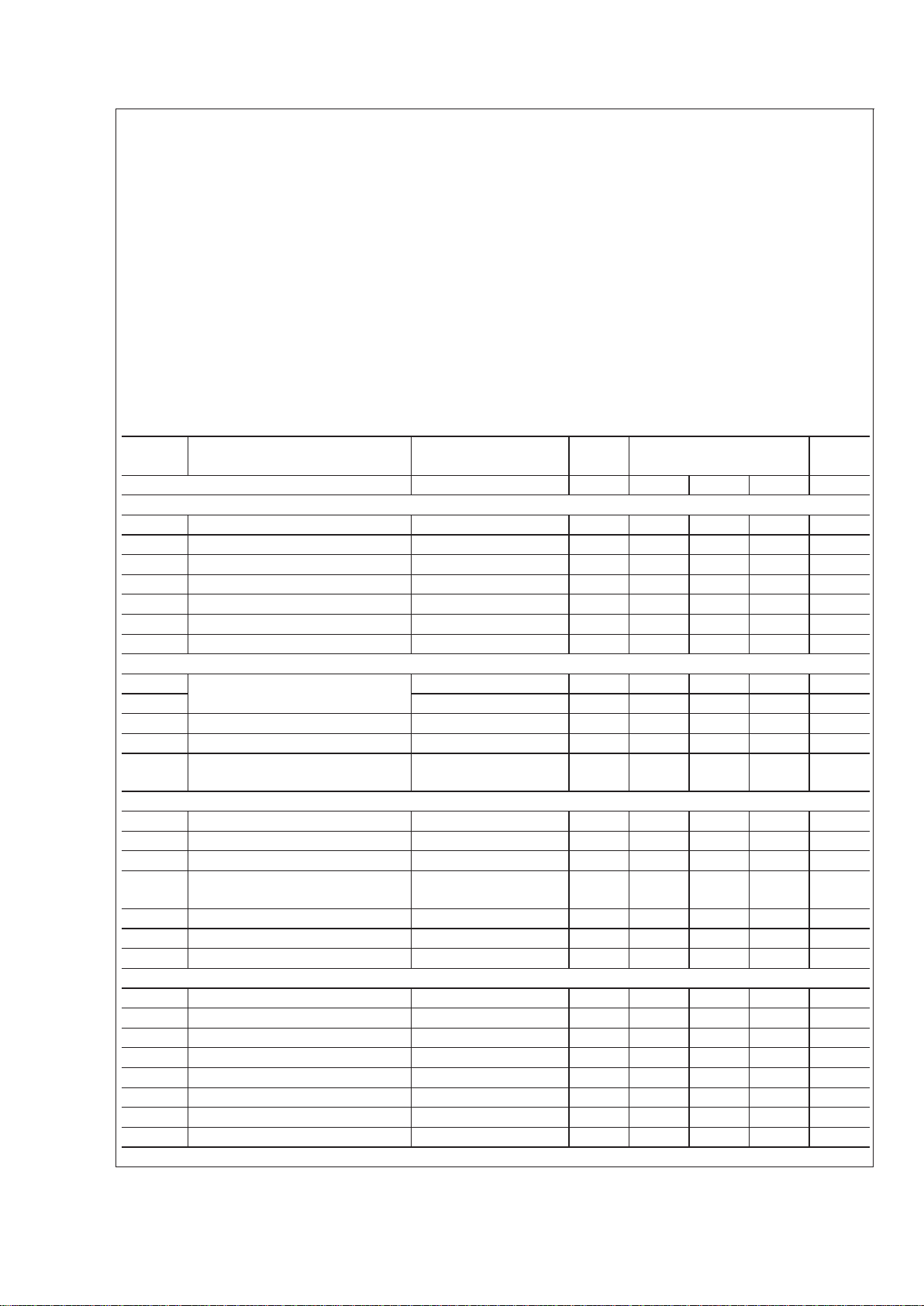
Connection Diagrams
01274619
Pinout
DIP & SOIC
01274618
Pinout
SOT 23-5
June 2001
CLC404 Wideband, High Slew Rate, Monolithic Op Amp
© 2001 National Semiconductor Corporation DS012746 www.national.com
Page 2
Absolute Maximum Ratings (Note 1)
If Military/Aerospace specified devices are required,
please contact the National Semiconductor Sales Office/
Distributors for availability and specifications.
Supply Voltage (V
CC
)
±
7V
I
OUT
Output is short circuit protected to
ground, but maximum reliability will
be maintained if I
OUT
does not
exceed... 60mA
Common Mode Input Voltage
±
V
CC
Differential Input Voltage 10V
Junction Temperature +150˚C
Operating Temperature Range −40˚C to +85˚C
Storage Temperature Range −65˚C to +150˚C
Lead Solder Duration (+300˚C) 10 sec
ESD rating (human body model) 500V
Operating Ratings
Thermal Resistance
Package (θ
JC
)(θ
JA
)
MDIP 65˚C/W 120˚C/W
SOIC 60˚C/W 140˚C/W
Electrical Characteristics
AV= +6, VCC=±5V, Rg&RL=100Ω,Rf= 500Ω; unless specified
Symbol Parameter Conditions Typ Max/Min Ratings
(Note 2)
Units
Ambient Temperature CLC404AJ +25˚C −40˚C +25˚C +85˚C
Frequency Domain Response
SSBW -3dB Bandwidth V
OUT
<
2V
PP
175
>
150
>
140
>
120 MHz
LSBW -3dB Large Signal V
OUT
<
5V
PP
165
>
140
>
140
>
110 MHz
Gain Flatness V
OUT
<
2V
PP
GFPL Peaking
<
40MHz 0
<
0.4
<
0.3
<
0.4 dB
GFPH Peaking
>
40MHz 0
<
0.7
<
0.5
<
0.7 dB
GFR Rolloff
<
75MHz 0.2
<
1.0
<
1.1
<
1.3 dB
LPD Linear Phase Deviation DC to 75MHz 0.5
<
1.0
<
1.0
<
1.2 deg
Time Domain Response
TRS Rise and Fall Time 2V Step 2.0
<
2.4
<
2.4
<
2.9 ns
TRL 5V Step 2.1
<
2.6
<
2.6
<
3.2 ns
TS Settling Time to
±
0.2% 2V Step 10
<
15
<
15
<
15 ns
OS Overshoot 2V Step 5
<
15
<
12
<
15 %
SR Slew Rate (Measured at A
V
+2)
(Note 4)
2600
>
2000
>
2000
>
2000 V/µs
Distortion And Noise Response
HD2 2nd Harmonic Distortion 2V
PP
,20MHz −53
<
−40
<
−45
<
−45 dBc
HD3 3rd Harmonic Distortion 2V
PP
,20MHz −60
<
−50
<
−50
<
−50 dBc
Equivalent Input Noise
SNF Noise Floor
>
1MHz −159
<
−157
<
−157
<
−156 dBm
(1Hz)
INV Integrated Noise 1MHz to 200MHz 40
<
45
<
45
<
50 µV
DG Differential Gain (Note 3) 0.07 ---%
DP Differential Phase (Note 3) 0.03 ---˚
Static, DC Performance
VIO Input Offset Voltage (Note 5) 2
<
±
9.0
<
±
5.0
<
±
10.0 mV
DVIO Average Temperature Coefficient 30
<
±
50 -
<
±
50 µV/˚C
IBN Input Bias Current (Note 5) Non Inverting 15
<
±
44
<
±
22
<
±
22 µA
DIBN Average Temperature Coefficient 150
<
±
275 -
<
±
200 nA/˚C
IBI Input Bias Current (Note 5) Inverting 15
<
±
40
<
±
18
<
±
22 µA
DIBI Average Temperature Coefficient 150
<
±
275 -
<
±
200 nA/C˚
PSRR Power Supply Rejection Ratio 52
>
45
>
48
>
45 dB
CMRR Common Mode Rejection Ration 50
>
44
>
46
>
44 dB
CLC404
www.national.com 2
Page 3
Electrical Characteristics (Continued)
AV= +6, VCC=±5V, Rg&RL=100Ω,Rf= 500Ω; unless specified
Symbol Parameter Conditions Typ Max/Min Ratings
(Note 2)
Units
ICC Supply Current (Note 5) No Load, Quiescent 11
<
12
<
12
<
12 mA
Miscellaneous Performance
RIN Non-Inverting Input Resistance 1000
>
250
>
500
>
1000 kΩ
CIN Capacitance 1
<
2
<
2
<
2pF
RO Output Impedence At DC 0.1
<
0.3
<
0.2
<
0.2 Ω
VO Output Voltage Range No Load
±
3.3
>
±
2.8
>
±
3.0
>
±
3.0 V
CMIR Common Mode Input Range For Rated Performance
±
2.2
>
±
1.4
>
±
1.8
>
±
2.0 V
IO Output Current
±
60
>
±
35
>
±
50
>
±
50 mA
Note 1: “Absolute Maximum Ratings” are those values beyond which the safety of the device cannot be guaranteed. They are not meant to imply that the devices
should be operated at these limits. The table of “Electrical Characteristics” specifies conditions of device operation.
Note 2: Max/min ratings are based on product characterization and simulation. Individual parameters are tested as noted. Outgoing quality levels are determined
from tested parameters.
Note 3: Differential gain and phase measured at A
V
+2, Rf500Ω,RL150Ω 1Vppequivalent video signal, 0-100 IRE, 40 IREpp, 0IRE = 0 volts, at 75Ω load and
3.58MHz. See text.
Note 4: See the text on the back of the datasheet.
Note 5: AJ-level: spec. is 100% tested at +25˚C, sample at 85˚C.
Ordering Information
Package Temperature Range
Industrial
Part Number Package Marking NSC
Drawing
8-pin plastic DIP −40˚C to +85˚C CLC404AJP CLC404AJP N08E
8-pin plastic SOIC −40˚C to +85˚C CLC404AJE CLC404AJE M08A
5-pin SOT −40˚C to +85˚C CLC404AJM5 A16 MA05A
CLC404
www.national.com3
Page 4

Typical Performance Characteristics
Frequency Response AV= +2V/V Frequency Response AV= +6V/V
01274601 01274602
Frequency Response AV= +20V/V Inverting Frequency Response
01274603 01274604
Bandwidth vs Load Capacitance Recommended RSvs Load Capacitance
01274605
01274606
CLC404
www.national.com 4
Page 5

Typical Performance Characteristics (Continued)
Large Signal Pulse Response 2nd Harmonic Dist. vs. Amplitude
01274607
01274608
3rd Harmonic Dist. vs. Amplitude Settling Time
01274609
01274610
2nd Harmonic Distortion CL= 25pF 3rd Harmonic Distortion CL= 25pF
01274611 01274612
CLC404
www.national.com5
Page 6

Typical Performance Characteristics (Continued)
Equivalent Input Noise Differential Gain and Phase vs. Load
01274613
01274614
CMRR and PSRR
01274615
CLC404
www.national.com 6
Page 7

Application Division
Slew Rate
Slew rate limiting is a nonlinear response which occurs in
amplifiers when the output voltage swing approaches hard,
abrupt limits in the speed at which it can change. In most
applications, this results in an easily identifiable “slew rate”
as well as a dramatic increase in distortion for large signal
levels. The CLC404 has been designed to provide enough
slew rate to avoid slew rate limiting in almost all circuit
configurations. The large signal bandwidth of 165MHz,
therefore, is nearly the same as the 175MHz small signal
bandwidth. The result is a low-distortion, linear system for
both small signals and large signals.
Slew rate and large signal performance in the CLC404 can
best be understood by first comparing the small and large
signal performance plots at a gain of +6. In the CLC404,
there is almost no difference between large and small signal
performance at this gain. Large signal performance in the
CLC404 at a gain of +6 is not slew rate limited. (In an
amplifier which is slew limiting, the large signal response
rolloff has an abrupt break indicating the onset of slew rate
limitation.)
The CLC404 reaches slew rate limits only for low
non-inverting gains. In other words, slew rate limiting is
constrained by common mode voltage swings at the input.
(This is different from traditional slew rate constraints.) The
large-signal frequency response plot at a gain of +2 shows a
break in the response, which shows that slew rate limit has
been reached. Note also that the frequency response plots
at gain of +21 show that the large signal and small signal
responses are nearly identical.
01274616
FIGURE 1. Recommended Non-Inverting Gain Circuit
01274617
FIGURE 2. Recommended Inverting Gain Circuit
CLC404
www.national.com7
Page 8

Differential Gain and Phase
Differential gain and phase are measurements useful primarily in composite video channels. Differential gain and phase
are measured by monitoring the gain and phase of a high
frequency carrier (3.58MHz for NTSC composite video) as
the output of the amplifier is swept over a range of DC
voltages. Any changes in gain and phase at the carrier
frequency are the desired measurement, differential gain
and phase.
Specifications for the CLC404 include differential gain and
phase. The test signals used are based on a 1V
PP
video
level. Test conditions used are the following.
DC sweep range: 0 to 100 IRE units (black to white)
Carrier: 3.58MHz at 40 IRE units peak to peak
The amplifier is specified for a gain of +2, and 150Ω load (for
a backmatched 75Ω system.) IRE amplitudes are referred to
75Ω at the load of a video system. This is a different condition from the rest of the specifications (A
V
= +6, Rf= 100Ω).
Source Impedance
For best results, source impedance in the non-inverting circuit configuration (see
Figure 1
) should be kept below 3kΩ
Above 3kΩ it is possible for oscillation to occur, depending
on other circuit parasitics. Depending on the signal source, a
resistor with a value of less than 3kΩ may be used to
terminate the non-inverting input to ground.
Feedback Resistor
In current-feedback op amps, the value of the feedback
resistor plays a major role in determining amplifier dynamics.
It is important to select the correct value resistor. The
CLC404 provides optimum performance with a 500Ω feedback resistor. Furthermore, the specifications shown on the
previous pages are valid only when a 500Ω feedback resistor is used. Selection of an incorrect value can lead to severe
rolloff in frequency-response (if the resistor value is too
large) or peaking or oscillation (if the value is too low).
Printed Circuit Layout
As with any high frequency device, a good PCB layout will
enhance performance. Ground plane construction and good
power supply bypassing close to the package are critical to
achieving full performance. In the non-inverting configuration, the amplifier is sensitive to stray capacitance to ground
at the inverting input. Hence, the inverting node connections
should be small with minimal coupling to the ground plane.
Shunt capacitance across the feedback resistor should not
be used to compensate for this effect.
Parasitic or load capacitance directly on the output will introduce additional phase shift in the loop degrading the loop
phase margin and leading to frequency response peaking. A
small series resistor before the capacitance effectively decouples this effect. The graphs on the preceding page illustrate the required resistor value and resulting performance
vs. capacitance.
Precision buffed resistors (PRP8351 series from Precision
Resistive Products) with low parasitic reactances were used
to develop the data sheet specifications. Precision carbon
composition resistors will also yield excellent results. Standard spirally-trimmed RN55D metal film resistors will work
with a slight decrease in bandwidth due to their reactive
nature at high frequencies.
Evaluation PC boards (part numbers CLC730013 for
through-hole and CLC 730027 for SOIC) for the CLC404 are
available.
CLC404
www.national.com 8
Page 9

Physical Dimensions inches (millimeters)
unless otherwise noted
NS Product Number M08A
NS Product Number MA05A
CLC404
www.national.com9
Page 10

Physical Dimensions inches (millimeters) unless otherwise noted (Continued)
NS Product Number N08E
LIFE SUPPORT POLICY
NATIONAL’S PRODUCTS ARE NOT AUTHORIZED FOR USE AS CRITICAL COMPONENTS IN LIFE SUPPORT
DEVICES OR SYSTEMS WITHOUT THE EXPRESS WRITTEN APPROVAL OF THE PRESIDENT AND GENERAL
COUNSEL OF NATIONAL SEMICONDUCTOR CORPORATION. As used herein:
1. Life support devices or systems are devices or
systems which, (a) are intended for surgical implant
into the body, or (b) support or sustain life, and
whose failure to perform when properly used in
accordance with instructions for use provided in the
labeling, can be reasonably expected to result in a
significant injury to the user.
2. A critical component is any component of a life
support device or system whose failure to perform
can be reasonably expected to cause the failure of
the life support device or system, or to affect its
safety or effectiveness.
National Semiconductor
Corporation
Americas
Email: support@nsc.com
National Semiconductor
Europe
Fax: +49 (0) 180-530 85 86
Email: europe.support@nsc.com
Deutsch Tel: +49 (0) 69 9508 6208
English Tel: +44 (0) 870 24 0 2171
Français Tel: +33 (0) 1 41 91 8790
National Semiconductor
Asia Pacific Customer
Response Group
Tel: 65-2544466
Fax: 65-2504466
Email: ap.support@nsc.com
National Semiconductor
Japan Ltd.
Tel: 81-3-5639-7560
Fax: 81-3-5639-7507
www.national.com
CLC404 Wideband, High Slew Rate, Monolithic Op Amp
National does not assume any responsibility for use of any circuitry described, no circuit patent licenses are implied and National reserves the right at any time without notice to change said circuitry and specifications.
 Loading...