

Page 1

PRELIMINARY
February 2002
CLC030
SMPTE 292M/259M Digital Video Serializer with Video
and Ancilliary Data FIFOs and Integrated Cable Driver
General Description
The CLC030 SMPTE 292M/259M Digital Video Serializer
with Ancilliary Data FIFO and Integrated Cable Driver is a
monolithic integrated circuit that encodes, serializes and
transmits bit-parallel digital video data conforming to SMPTE
125M and 267M standard definition, 10-bit wide component
video and SMPTE 260M, 274M, 295M and 296M highdefinition, 20-bit wide component video standards. The
CLC030 operates at SMPTE 259M serial data rates of
270 Mbps, 360 Mbps, the SMPTE 344M (proposed) serial
data rate of 540 Mbps; and the SMPTE 292M serial data
rates of 1483.5 and 1.485 Gbps. The serial data clock frequency is internally generated and requires no external frequency setting, trimming or filtering components*.
Functions performed by the CLC030 include: parallel-toserial data conversion, SMPTE standard data encoding,
NRZ to NRZI data format conversion, serial data clock generation and encoding with the serial data, automatic video
rate and format detection, ancilliary data packet storage,
manipulation and insertion, and serial data output driving.
The CLC030 has circuitry for automatic EDH/CRC character
and flag generation and insertion per SMPTE RP-165 (standard definition) or SMPTE 292M (high definition). Optional
LSB dithering is implemented which prevents pathological
pattern generation. Unique to the CLC030 are its video and
ancilliary data FIFOs. The video FIFO allows from 0 to 4
parallel data clock delays to be inserted in the data path for
video timing purposes. The ancilliary data port and on-chip
FIFO and control circuitry offer elegant handling and insertion of ancilliary datapacketsandchecksumsin the ancilliary
data space. The CLC030 also has an exclusive built-in selftest (BIST) and video test pattern generator (TPG) with SD
and HD component video test patterns: reference black, PLL
and EQ pathologicals and colour bars in 4:3 and 16:9 raster
formats for NTSC and PAL standards*. The colour bar patterns feature optional bandwidth limiting coding in the
chroma and luma transitions.
The CLC030 has a unique multi-function I/O port which
provides access to control and configuration signals and
data. This port may be programmed to provide external
access to control functions and data for use as inputs and
outputs. This allows the designer greater flexibility in tailoring
the CLC030 to the desired application. At power-up or after a
reset command, the CLC030 is auto-configured to a default
operating condition. Separate power pins for the output
driver, PLL and the serializer improve power supply rejection, output jitter and noise performance.
The CLC030’s internal circuitry is powered from +2.5V and
the I/O circuitry from a +3.3V supply. Power dissipation is
typically 430mW at 1.485Gbps including two 75Ω ACcoupled and back-matched output loads. The device is packaged in a 64-pin TQFP.
Features
n SDTV/HDTV serial digital video standard compliant
n Supports 270 Mbps, 360 Mbps, 540 Mbps, 1.4835Gbps
and 1.485 Gbps SDV data rates with auto-detection
n LSB dithering option
n No external serial data rate setting or VCO filtering
components required*
n Fast PLL lock time:
n Adjustable depth video FIFO for timing alignment
n Built-in self-test (BIST) and video test pattern generator
(TPG)*
n Automatic EDH/CRC word and flag generation and
insertion
n On-chip ancilliary data FIFO and insertion control
circuitry
n Flexible control and configuration I/O port
n LVCMOS compatible data and control inputs and
outputs
n 75Ω ECL-compatible, differential, serial cable-driver
outputs
n 3.3V I/O power supply, 2.5V logic power supply
operation
n Low power: typically 430mW
n 64-pin TQFP package
n Commercial temperature range 0˚C to +70˚C
*
Patent applications made or pending.
<
150µs typical at 1.485 Gbps
Applications
n SDTV/HDTV parallel-to-serial digital video interfaces for:
— Video cameras
— VTRs
— Telecines
— Digital video routers and switchers
— Digital video processing and editing equipment
— Video test pattern generators and digital video test
equipment
— Video signal generators
CLC030 SMPTE 292M/259M Digital Video Serializer with Video and Ancilliary Data FIFOs and
Integrated Cable Driver
Order Number CLC030VEC 64-Pin TQFP
© 2002 National Semiconductor Corporation DS200003 www.national.com
NS Package Number
VEC-64A
Page 2
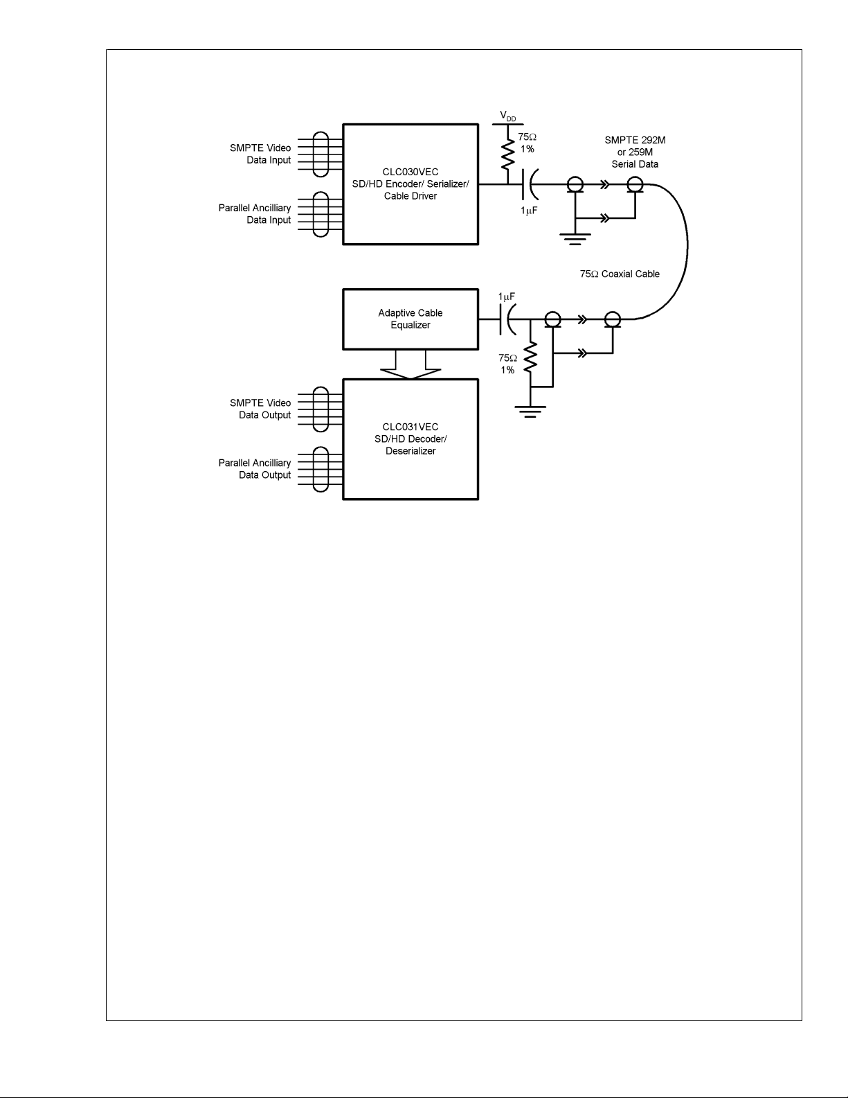
Typical Application
CLC030
DS200003-1
www.national.com 2
Page 3
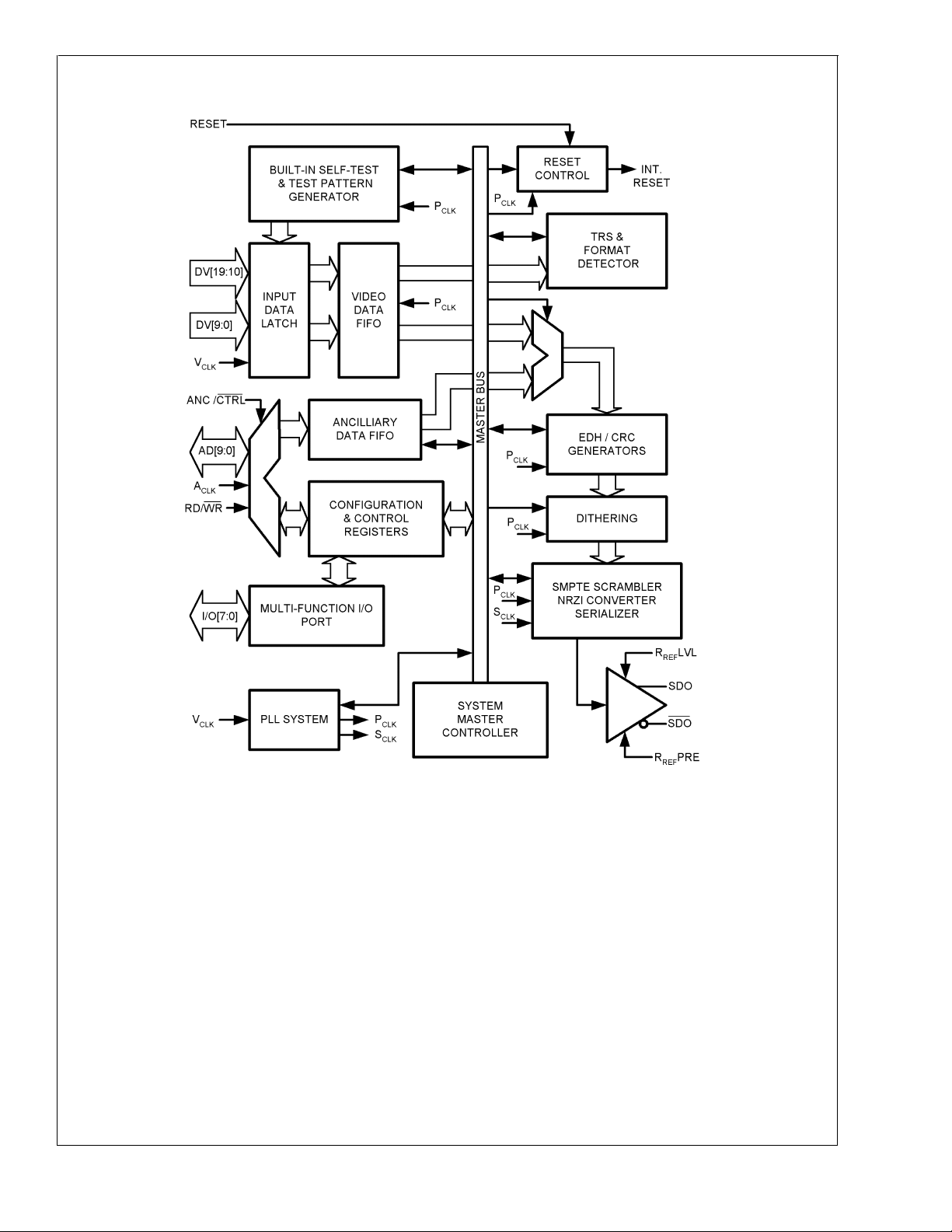
Block Diagram
CLC030
DS200003-2
www.national.com3
Page 4
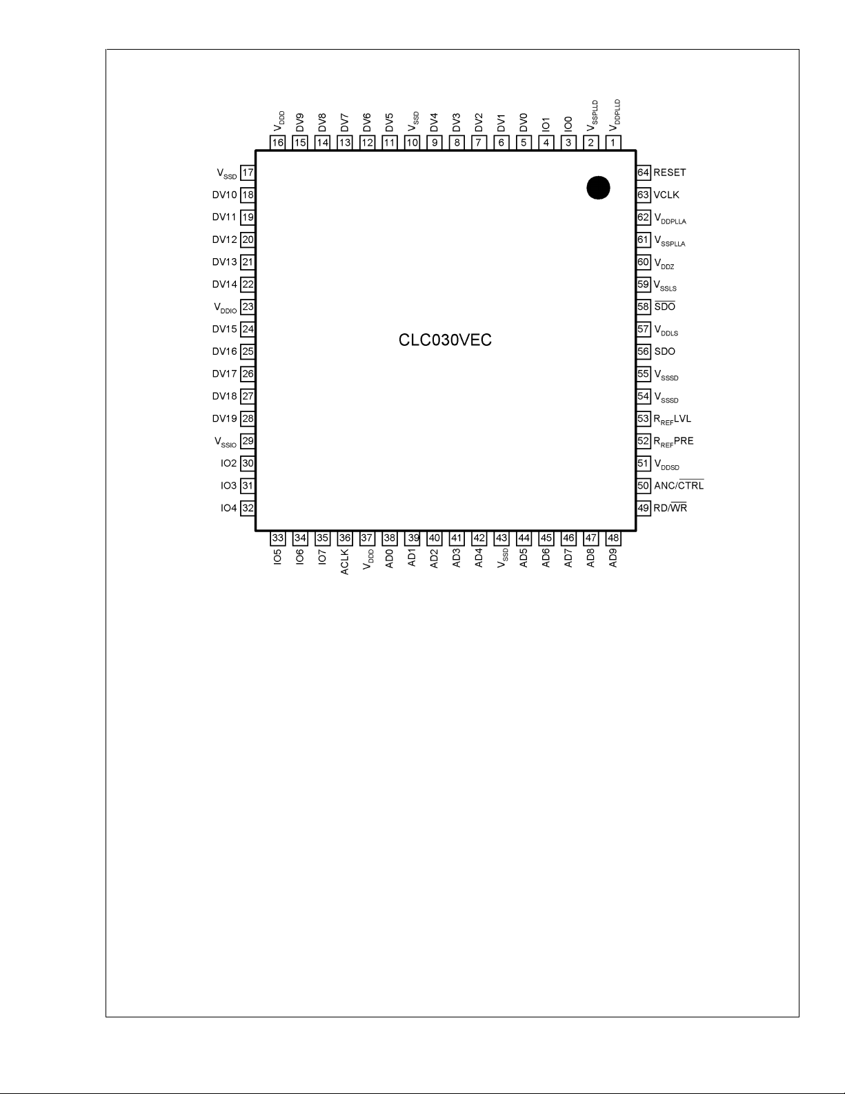
Connection Diagram
CLC030
64-Pin TQFP
Order Number CLC030VEC
See NS Package Number VEC-64A
DS200003-3
www.national.com 4
Page 5
CLC030
Absolute Maximum Ratings (Note 1)
It is anticipated that this device will not be offered in
a military qualified version. If Military/Aerospace speci-
fied devices are required, please contact the National
Semiconductor Sales Office / Distributors for availability
and specifications.
CMOS Input Current (single input):
Vi=V
Vi=V
CMOS Output Source/Sink Current:
−0.15V: −5 mA
SSIO
+0.15V: +5 mA
DDIO
±
10 mA
SDO Output Sink Current: 40 mA
Package Thermal Resistance
CMOS I/O Supply Voltage
(V
DDIO–VSSIO
): 4.0V
SDO Supply Voltage
(V
DDSD–VSSSD
): 4.0V
Digital Logic Supply Voltage
(V
DDD–VSSD
): 3.0V
PLL Supply Voltage
(V
DDPLL–VSSPLL
): 3.0V
CMOS Input Voltage
(Vi):
CMOS Output Voltage
(Vo):
V
V
SSIO
V
SSIO
V
DDIO
DDIO
−0.15V to
+0.15V
−0.15V to
+0.15V
@
0 LFM Airflow 47˚C/W
θ
JA
@
500 LFM Airflow 27˚C/W
θ
JA
θ
JC
6.5˚C/W
Storage Temp. Range: −65˚C to +150˚C
Junction Temperature: +150˚C
Lead Temperature (Soldering 4 Sec): +260˚C
ESD Rating (HBM): 2 kV
ESD Rating (MM): 250V
Recommended Operating Conditions
Symbol Parameter Conditions Reference Min Typ Max Units
V
V
V
V
V
V
T
t
JIT
DDIO
DDSD
DDD
DDPLL
IL
IH
A
CMOS I/O Supply
V
DDIO−VSSIO
Voltage
SDO Supply Voltage V
Digital Logic Supply
DDSD−VSSSD
V
DDD–VSSD
Voltage
PLL Supply Voltage V
DDPLL–VSSPLL
CMOS Input Voltage,
Low Level
CMOS Input Voltage
High Level
Operating Free Air
Temperature
Video Clock Jitter V
CLK
3.150 3.300 3.450 V
3.150 3.300 3.450 V
2.375 2.500 2.625 V
2.375 2.500 2.625 V
V
SSIO
V
DDIO
0 +70 ˚C
100 ps
V
V
P-P
DC Electrical Characteristics
Over Supply Voltage and Operating Temperature ranges, unless otherwise specified (Notes 2, 3).
Symbol Parameter Conditions Reference Min Typ Max Units
V
IH
V
IL
I
IH
I
IL
V
OH
V
OL
V
SDO
I
DD
(3.3V)
I
DD
(3.3V)
Input Voltage High Level All LVCMOS
Input Voltage Low Level V
Input Current High Level VIH=V
Input Current Low Level VIL=V
CMOS Output Voltage
DDIO
SSIO
IOH= −6.6 mA All LVCMOS
High Level
CMOS Output Voltage
IOL= +6.6 mA
Inputs
Outputs
Low Level
Serial Driver Output
Voltage
Power Supply Current,
3.3V Supply, Total
Test Circuit, Test Loads
Shall Apply
V
= 27 MHz, NTSC
CLK
Colour Bar Pattern, Test
SDO, SDO
V
DDIO,VDDSD
Circuit, Test Loads Shall
Apply
Power Supply Current,
3.3V Supply, Total
V
= 74.25 MHz, NTSC
CLK
Colour Bar Pattern, Test
V
DDIO,VDDSD
Circuit, Test Loads Shall
Apply
2.0 V
SSIO
DDIO
0.8 V
+90 +150 µA
−1 −20 µA
2.4 2.7 V
V
V
SSIO
SSIO
+0.3
DDIO
V
SSIO
+0.5V
720 800 880 mV
48 65 mA
66 90 mA
www.national.com5
V
V
V
P-P
Page 6
DC Electrical Characteristics (Continued)
Over Supply Voltage and Operating Temperature ranges, unless otherwise specified (Notes 2, 3).
CLC030
Symbol Parameter Conditions Reference Min Typ Max Units
I
DD
(2.5V)
Power Supply Current,
2.5V Supply, Total
V
= 27 MHz, NTSC
CLK
Colour Bar Pattern, Test
Circuit, Test Loads Shall
V
DDD,VDDZ
V
DDPLL
,
66 85 mA
Apply
I
DD
(2.5V)
Power Supply Current,
2.5V Supply, Total
V
= 74.25 MHz, NTSC
CLK
Colour Bar Pattern, Test
Circuit, Test Loads Shall
V
DDD,VDDZ
V
DDPLL
,
85 110 mA
Apply
AC Electrical Characteristics
Over Supply Voltage and Operating Temperature ranges, unless otherwise specified (Note 3).
Symbol Parameter Conditions Reference Min Typ Max Units
f
VCLK
DC
V
f
ACLK
DC
A
t
r,tf
BR
SDO
tr,t
f
t
r,tf
t
j
t
j
t
LOCK
t
LOCK
t
S
t
H
t
S
t
H
Note 1: “Absolute Maximum Ratings” are those parameter values beyond which the life and operation of the device cannot be guaranteed. The stating herein of
these maximums shall not be construed to imply that the device can or should be operated at or beyond these values. The table of “Electrical Characteristics”
specifies acceptable device operating conditions.
Note 2: Current flow into device pins is defined as positive. Current flow out of device pins is defined as negative. All voltages are referenced to V
Note 3: Typical values are stated for V
Note 4: Spec. is guaranteed by design.
Note 5: R
Note 6: R
Note 7: Measured from rising-edge of first DV
Note 8: Average value measured between rising edges computed over at least one video field.
Note 9: Intrinsic timing jitter is measured in accordance with SMPTE RP 184-1996, SMPTE RP 192-1996 and the applicable serial data transmission standard,
SMPTE 259M-1997 or SMPTE 292M (proposed). A colour bar test pattern is used. The value of f
344M or 1,485 MHz for SMPTE 292M serial data rates. See Timing Jitter Bandpass section.
Parallel Video Clock
Frequency
Video Clock Duty
Cycle
Ancilliary Clock
Frequency
Ancilliary Clock Duty
Cycle
Input Clock and Data
Rise Time, Fall Time
10%–90% V
V
CLK
V
CLK
A
CLK
A
CLK
CLK,ACLK
,AD
DV
N
27 74.25 MHz
45 50 55 %
V
CLK
45 50 55 %
,
N
1.0 1.5 3.0 ns
Serial Data Rate (Notes 5, 6) SDO, SDO 270 1,485 M
Rise Time, Fall Time 20%–80%, (Note 6) SDO, SDO 270 ps
Rise Time, Fall Time 20%–80%, (Note 5) SDO, SDO 500 ps
Output Overshoot (Note 4) SDO, SDO
Serial Output Jitter,
270 M
, (Notes 5, 9, 10) SDO, SDO
bps
Intrinsic
Serial Output Jitter,
1,485 M
, (Notes 6, 9, 10) SDO, SDO
bps
Intrinsic
5%
200 ps
120 ps
Lock Time (Notes 5, 7) (SD Rates) 15 ms
Lock Time (Notes 6, 7) (HD Rates) 15 ms
Setup Time, Video
Data
Hold Time, Video
Data
Setup Time, Anc.
Data Port
Hold Time, Anc. Data
Port
=75Ω, AC-coupled@270 M
L
=75Ω, AC-coupled@1,485 M
L
Timing Diagram, (Note 4) DVNto V
Timing Diagram, (Note 4) V
Timing Diagram, (Note 4) ADNto A
Timing Diagram, (Note 4) A
DDIO=VDDSD
LVL = R
bps,RREF
bps,RREF
cycle until Lock Detect output goes high (true). Lock time includes format detection time plus PLL lock time.
CLK
= +3.3V, V
LVL = R
DDD=VDDPLL
PRE = 4.75 kΩ 1%, See Test Loads and Test Circuit.
REF
PRE = 4.75 kΩ 1%, See Test Loads and Test Circuit.
REF
= +2.5V and TA= +25˚C.
CLK
to DV
CLK
CLK
SCLK
N
CLK
to AD
N
is 270 MHz or 360 MHz for SMPTE 259M, 540MHz for SMPTE
1.5 2.0 ns
1.5 2.0 ns
1.5 2.0 ns
1.5 2.0 ns
SS
MHz
bps
P-P
P-P
=0V.
www.national.com 6
Page 7
AC Electrical Characteristics (Continued)
Note 10: Intrinsic jitter is defined in accordance with SMPTE RP 184-1996 as: jitter at an equipment output in the absence of input jitter. As applied to this device,
the input port is V
and the output port is SDO or SDO.
CLK
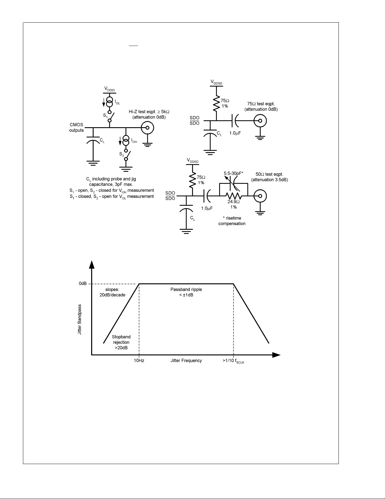
Test Loads
CLC030
Timing Jitter Bandpass
DS200003-4
DS200003-6
www.national.com7
Page 8
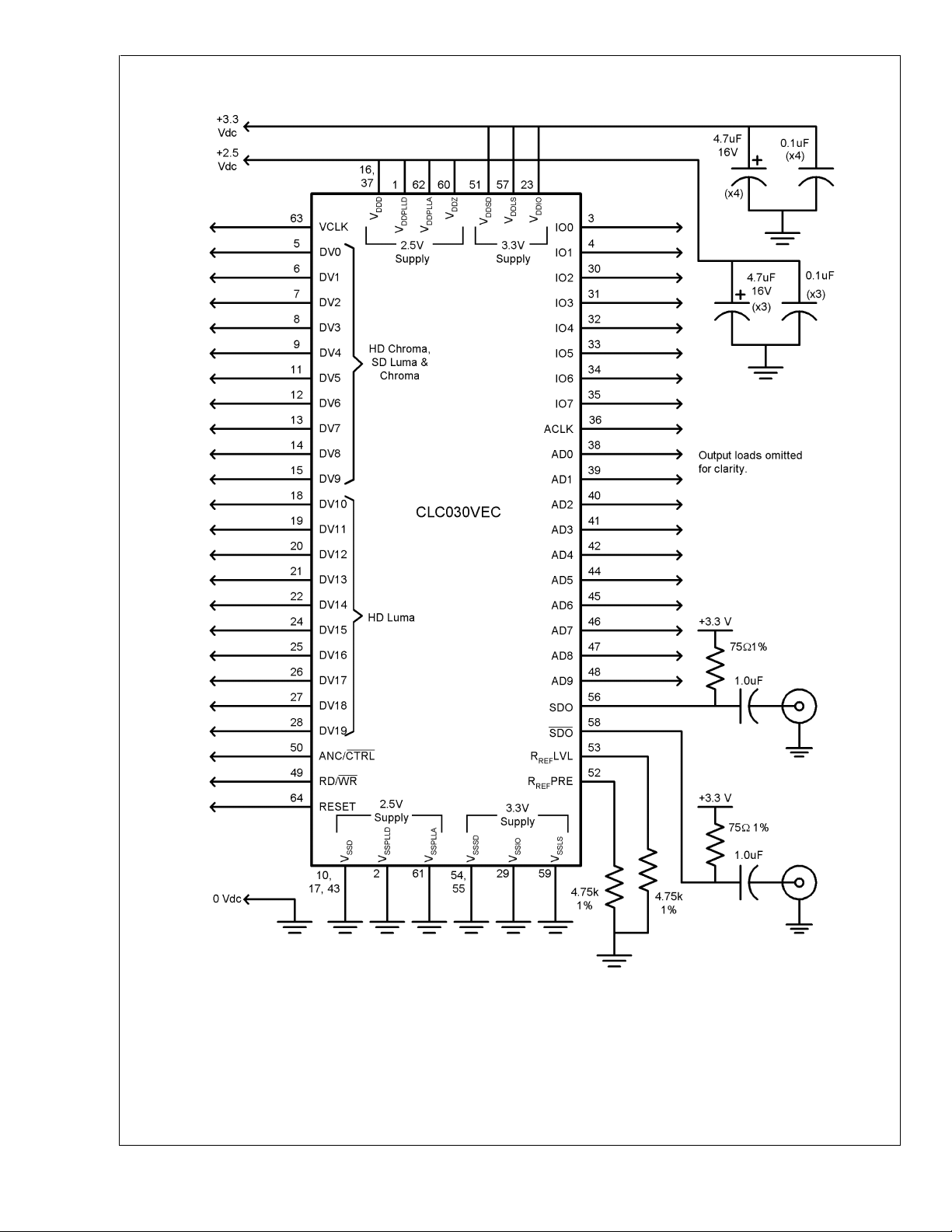
Test Circuit
CLC030
www.national.com 8
DS200003-7
Page 9
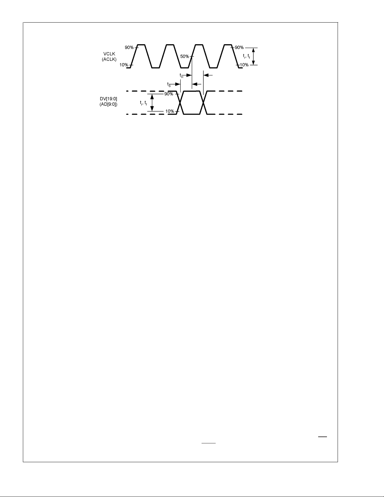
Timing Diagram
Device Operation
The CLC030 SDTV/HDTV Serializer is used in digital video
signal origination equipment: cameras, video tape recorders,
telecines and video test and other equipment. It converts
parallel SDTV or HDTV component digital video signals into
serial format. Logic levels within this equipment are normally
produced by LVCMOS logic devices. The encoder produces
serial digital video (SDV) signals conforming to SMPTE
259M, SMPTE 344M (proposed) or SMPTE 292M. The
CLC030 operates at parallel data rates of 27.0 MHz, 36.0
MHz, 54.0 MHz, 74.176MHz and 74.25 MHz. Corresponding
serial data rates are 270 Mbps, 360 Mbps, 540 Mbps,
1.4835Gbps and 1.485 Gbps. Segmented frame formats are
not supported.
VIDEO DATA PATH
The input data register accepts 10-bit standard definition or
20-bit high definition parallel data and associated clock signals having LVCMOS-compatible signal levels. All parallel
video data inputs, DV[19:0], have internal pull-down devices. VCLK does not have an internal pull-down device.
Parallel video data may conform to any of several SMPTE
standards: 125M, 267M, 260M, 274M, 295M or 296M. Segmented frame formats are not supported. For HDTV data,
the upper 10 bits of the DV input are luminance (luma)
information and the lower 10 bits are colour difference
(chrominance or chroma) information. For SDTV data, the
lower order 10 bits contain both luma and chroma information. Output from this register feeds the video FIFO, video
format detection circuit, TRS character detector, SMPTE
scrambler, EDH/CRC generators, serializer/NRZI converter
and the device control system.
Data from the input data register passes into a 4-register
deep video FIFO prior to encoding and other processing.
The depth of this FIFO is set by a word written into the
VIDEO FIFO Depth[2:0] bits in the ANC 0 control register.
The video format detector automatically determines the
raster characteristics (video data format) of the parallel input
data and configures the CLC030 to properly handle the data.
This assures that the data will be properly formatted, that the
correct data rate is selected and that ancilliary data, line
numbers (HD) and CRC/EDH data are correctly inserted.
Indication of the standard being processed is stored in the
FORMAT[4:0] bits in the FORMAT 1 control data register.
This format data can be programmed for output on the
multi-function I/O port.
The CLC030 may be configured to operate at a single video
format by writing the appropriate FORMAT SET[4:0] control
data into the FORMAT 0 control register. Also, the CLC030
may be configured to handle only the standard-definition
DS200003-8
data formats by setting the SD ONLY bit or only the highdefinition data formats by setting the HD ONLY bit in the
FORMAT 0 control register. When both of these bits are
reset the part automatically detects the data rate and range.
The TRS character detector processes the timing reference signals which control raster framing. The TRS detector
supplies control signals to the system controller to identify
the presence of the valid video data. The system controller
supplies necessary control signals to the EDH/CRC control
block. TRS character LSB-clipping as prescribed in ITU-R
BT.601 is used. LSB-clipping causes all TRS characters with
a value between 000h and 003h to be forced to 000h and all
TRS characters with a value between 3FCh and 3FFh to be
forced to 3FFh. Clipping is done prior to scrambling and
EDH/CRC character generation.
The CLC030 incorporates circuitry that implements the proposed SMPTE recommended practice and method for LSB
dithering. Control of this circuitry is via the Dither Enable bit
in the VIDEO INFO 0 control register. Dithering can be
selectively enabled during the vertical blanking interval by
use of the V Dither Enable bit in the VIDEO INFO 0 control
register. The initial condition of Dither Enable and V Dither
Enable is OFF.
The SMPTE scrambler accepts 10-bit standard definition or
20-bit high definition parallel video data and encodes it using
the polynomial X
standard in SMPTE 259M, SMPTE 344M (proposed) or
SMPTE 292M. The data is then serialized and sent to the
NRZ-to-NRZI converter before being output. The transmission bit order is LSB-first.
The NRZ-to-NRZI converter accepts NRZ serial data from
the SMPTE scrambler. The data is converted to NRZI format
using the polynomial (X + 1). The converter’s output goes to
the output cable driver amplifier.
ANCILLIARY/CONTROL DATA PATH
The Ancilliary and Control Data Port serves two functions
in the CLC030. It is used to selectively load ancilliary data
into the Ancilliary Data FIFO for insertion into the video data
stream. The utilization and flow of ancilliary data within the
device is managed by a system of control bits, masks and
IDs in the control data registers. This port also provides
read/write access to contents of the configuration and control registers. Configuration of the multi-function I/O Port is
also controlled by information stored in the control data
registers. Ancilliary and control data are input via the 10-bit
Ancilliary/Control Data Port, AD[9:0]. The signals RD/WR,
ANC/CTRL and ACLK control data flow through the port.
The operation and frequency of ACLK is completely inde-
9+X4
+ 1 as specified in the respective
CLC030
www.national.com9
Page 10

Device Operation (Continued)
pendent of the video data clock, VCLK. Inputs AD[9:0],
CLC030
RD/WR and ANC/CTRL have internal pull down devices.
ACLK does not have an internal pull down device.
Control Data Read Functions
Control data is input to and output from the CLC030 using
the lower-order 8 bits AD[7:0] of the Ancilliary/Control Data
Port. This control data initializes, monitors and controls operation of the CLC030. The upper two bits AD[9:8] of the
port function as handshaking signals with the device accessing the port. AD[9:8] must be driven as 00b (0XXh, where
XX are AD[7:0]) when either a control register read or write
address is being written to the port. AD[9:8] must be driven
as 11b (3XXh, where XX are AD[7:0]) when control data is
being written to the port. When control data is being read
from the port, the CLC030 will output AD[9:8] as 10b (2XXh,
where XX are output data AD[7:0]) and may be ignored by
the monitoring system.
Note: When power is first applied to the device or after it is
reset, the Ancilliary and Control Data Port must be initialized to receive data. This is done by toggling ACLK three (3)
times.
Figure 1
reading control data from the ancilliary/control data port.
Control data read mode is invoked by making the
ANC/CTRL input low and the RD/WR input high. The 8-bit
address of the control register set to be accessed is input to
the port on bits AD[7:0]. The address is captured on the
rising edge of ACLK. When a control register read address
is being written to the port, AD[9:8] must be driven as 00b
(0XXh, where XX are AD[7:0]). When control data is being
read from the port, the CLC030 will output AD[9:8] as 10b
(2XXh, where XX are output data AD[7:0]) and may be
ignored by the monitoring system. Data being output from
the selected register is driven by the port immediately following the rising edge of ACLK or when the address signals are
removed. For optimum system timing, the address signals
driving the port should be removed immediately after the
address is clocked into the device and before or coincident
with the falling edge of ACLK at the end of the address
cycle. Output data remains stable until the next rising edge
of ACLK and may be read by external devices at any time
after the removal of the address signal. This second clock
resets the port from drive to receive mode and readies the
port for another access cycle.
shows the sequence of clock and control signals for
Example: Read the Full-field Flags via the AD port.
1. Set ANC/CTRL to a logic-low.
2. Set RD/WR to a logic-high.
3. Present 001h to AD[9:0] as the register address.
4. Toggle ACLK.
5. Release the bus driving the AD port.
6. Read the data present on the AD port. The Full-field
Flags are bits AD[4:0].
7. Toggle ACLK to release the AD port.
Control Data Write Functions
Figure 2
writing control data to the ancilliary/control data port. The
control data write mode is similar to the read mode. Control data write mode is invoked by making the ANC/CTRL
input low and the RD/WR input low. The 8-bit address of the
control register set to be accessed is input to the port on bits
AD[7:0]. The address is captured on the rising edge of
ACLK. The address data is removed after being clocked into
the device or before the falling edge of ACLK. Next, the
control data is presented to the port bits AD[7:0] and written
into the selected register on the next rising edge of ACLK.
When a control register write address is being written to the
port, AD[9:8] must be driven as 00b (0XXh, where XX are
AD[7:0]). When control data is being written to the port,
AD[9:8] must be driven as 11b (3XXh, where XX are
AD[7:0]). Control data written into the registers may be read
out non-destructively in most cases.
Example: Setup (without enabling) the TPG Mode via the
AD port using the 1125 line, 30 frame, 74.25MHz, interlaced
component (SMPTE 274M) colour bars as test pattern. The
TPG may be enabled after setup using the Multi-function I/O
port or by the control registers.
1. Set ANC/CTRL to a logic-low.
2. Set RD/WR to a logic-low.
3. Present 00Dh to AD[9:0] as the Test 0 register address.
4. Toggle ACLK.
5. Present 027h to AD[9:0] as the register data.
6. Toggle ACLK.
shows the sequence of clock and control signals for
www.national.com 10
Page 11

Device Operation (Continued)
FIGURE 1. Control Data Read Timing (2 read and 1 write cycle shown)
CLC030
DS200003-9
FIGURE 2. Control Data Write Timing
Ancilliary Data Functions
The CLC030 can insert Ancilliary Data into the serial data
stream. This ancilliary data and related control characters
are defined in the relevant SMPTE standards and may reside in the horizontal and vertical blanking intervals. The
data can consist of different types of message packets including audio data. The serial ancilliary data space must be
formatted according to SMPTE 291M. The CLC030 supports
ancilliary data in the chrominance channel (C’r/C’b) only for
high-definition operation. Ancilliary data for standard definition follows the requirements of SMPTE 125M.
Figure 3
shows the sequence of clock, data and control
signals for writing ancilliary data to the port. In ancilliary data
write mode, 10-bit Ancilliary Data is written into the port
DS200003-10
using bits AD[9:0] and routed to the ancilliary data FIFO.
From the FIFO, the ancilliary data can be written into the
ancilliary data spaces in the serial video data stream. Ancilliary data write mode is invoked by making the ANC/CTRL
input high and the RD/WR input low. Data presented to the
port on a falling edge of ACLK is written into the FIFO on the
next rising edge of ACLK.Ancilliary data may only be written
to the FIFO when in the ancilliary data mode. Ancilliary data
cannot be read from the port.
Admission of ancilliary data to and insertion into the video
data stream from the FIFO is controlled by a system of
masking and control bits in the control registers. The details
and functions of these control registers and bits is explained
later in this datasheet.
www.national.com11
Page 12

Device Operation (Continued)
CLC030
FIGURE 3. Ancilliary Data Write Timing
MULTI-FUNCTION I/O PORT
The multi-function I/O port can be configured to provide
immediate access to many control and indicator functions
within the CLC030 configuration and control registers. The
individual pins comprising this port are assigned as input or
output for selected bits in the control data registers. The
multi-function I/O port is configured by way of an 8x6-bit
register bank, configuration and control registers I/O pin 0
CONFIG through I/O pin 7 CONFIG. The contents of these
registers determine whether the port bits function as inputs
or outputs and to which register element each port bit is
assigned. Port bits may be assigned to access different
register elements or any or all port bits may be assigned to
access the same register element (an unlikely or unusual
situation). Controls and indicators that are accessible by the
port and their corresponding selection addresses are given
in the I/O Pin Configuration Register Addresses,
Table 2
Caution: When writing data into the control registers via the
multi-function I/O port, ACLK must be toggled to register the
data as shown in
ACLK when reading data from the multi-function I/O port.
Example: Program multi-function I/O port bit-0 as the CRC
Luma Error bit output.
1. Set ANC/CTRL to a logic-low.
2. Set RD/WR to a logic-low.
3. Present 00Fh to AD[9:0] as the I/O PIN 0 CONFIG
4. Toggle ACLK.
5. Present 310h to AD[9:0] as the register data.
6. Toggle ACLK.
EDH/CRC SYSTEM
The CLC030 has EDH and CRC character generation and
insertion circuitry. The EDH system functions as described
in SMPTE Recommended Practice RP-165. The CRC sys-
gives the control register bit assignments.
Figure 4
. It is not necessary to toggle
register address.
FIGURE 4. I/O Port Data Write Timing
Table 6
DS200003-12
DS200003-11
tem functions as specified in SMPTE 292M. The EDH/CRC
polynomial generators accept parallel data from the input
register and generate the EDH and CRC check words for
insertion in the serial data. Incoming parallel data is checked
for errors and the EDH flags are updated automatically. EDH
check words and status flags for SDTV data are generated
using the polynomial X
16+X12+X6
+ 1 per SMPTE RP165.
EDH check words are inserted in the serial data stream at
the correct positions in the ancilliary data space and formatted per SMPTE 291M. Generation and automatic insertion of
the EDH check words is controlled by EDH Force and EDH
Enable bits in the control registers. After a reset, the initial
state of all EDH and CRC check characters is 00h.
The SMPTE 292M high definition video standard employs
CRC (cyclic redundancy check codes) error checking instead of EDH. The CRC consists of two 18-bit words gener-
.
ated using the polynomial X
18+X5+X4
+ 1 per SMPTE
292M. One CRC is used for luminance and one for chrominance data. CRC data is inserted at the required place in the
video data according to SMPTE 292M. The CRCs appear in
the data stream following the EAV and line number characters.
EDH and CRC errors are reported in the EDH0, EDH1, and
EDH2 register sets of the configuration and control registers.
PHASE-LOCKED LOOP SYSTEM
The phase-locked loop (PLL) system generates the output
serial data clock at 10x (standard definition) or 20x (high
definition) the parallel data clock frequency. This system
consists of a VCO, divider chain, phase-frequency detector
and internal loop filter. The VCO free-running frequency is
internally set. The PLL automatically generates the appropriate frequency for the serial clock rate using the parallel data
clock (VCLK) frequency as its reference. Loop filtering is
internal to the CLC030. The VCO has separate analog and
digital power supply feeds: V
V
DDPLLD
pin 1, and V
SSPLLD
DDPLLA
pin 62, V
SSPLLA
pin 61,
pin 2. These may be separately
supplied power via external low-pass filters, if desired. PLL
acquisition time is less than 200µs
@
1,485 Mbps. The VCO
halts when VCLK signal is not present or is inactive.
A LOCK DETECT indicator function is available as a bit in
the VIDEO INFO 0 control registers. LOCK DETECT is a
logic-1 when the PLL is locked and can be assigned as an
output on the multifunction I/O port. The power-on or reset
default assigns LOCK DETECT as I/O Port bit 4. This function also includes logic to check the stability of the device
after the digital logic reset is released following PLL lock. If
the system is not fully stable, the logic is automatically reset.
LOCK DETECT also combines the function of indicating that
www.national.com 12
Page 13

Device Operation (Continued)
the CLC030 has detected the video format being received.
This format detect function involves determination of the
major raster parameters such as line length, number of video
lines in a frame, and so forth. This is done so that information
like line numbering can be correctly inserted. The PLL itself
will have locked in 200 microseconds (HD rates) or less.
However, resolution of all raster parameters may take the
majority of a frame.
SERIAL DATA OUTPUT DRIVER
The serial data outputs provide low-skew complimentary or
differential signals. The output buffer is a current-mode design and is intended to drive AC-coupled and terminated,
75Ω coaxial cables. The driver automatically adjusts rise and
fall times depending upon the data rate being processed.
Output levels are 800 mV
loads. The 75Ω resistors connected to the SDO outputs
function both as drain-load and back-matching resistors.
Series back-matching resistors are not used with this output
type.
The serial output level is controlled by the value of R
and R
The R
PRE connected to pin 53 and pin 52, respectively.
REF
LVL resistor sets the peak-to-peak level of the
REF
output signal to the required SMPTE nominal level. The
R
PRE resistor sets the value of a pre-emphasis current
REF
which is active during the rise and fall times of the HD-rate
output signal. The value of R
±
1%. The value of R
REF
voltage present at these pins is approximately +1.3Vdc. The
rise and fall times of this output buffer design automatically
adjust and are different for the HD and SD data rate conditions. The output buffer is quiescent when the device is in an
out-of-lock condition. The output will become active after the
PLL is locked and a valid format has been detected. Separate power feeds are provided for the serial output driver:
V
, pins 54, 55, and 59; V
SSSD
57.
CAUTION: This output buffer is not designed or specified for
driving 50Ω or other impedance loads.
POWER SUPPLIES, POWER-ON-RESET AND RESET
INPUT
The CLC030 requires two power supplies, 2.5V for the core
logic functions and 3.3V for the I/O functions. The supplies
must be applied to the device in proper sequence. The 3.3V
supply must be applied prior to or coincident with the 2.5V
supply.Application of the 2.5V supply must not precede the
3.3V supply. It is recommended that the 3.3V supply be
configured or designed so as to control application of the
2.5V supply in order to satisfy this sequencing requirement.
The CLC030 has an automatic, power-on-reset circuit. Re-
set initializes the device and clears TRS detection circuitry,
all latches, registers, counters and polynomial generators,
sets the EDH/CRC characters to 00h and disables the serial
output.
Table 1
lists the initial conditions of the configuration
and control registers. An active-HIGH-true, manual reset
input is available at pin 64. The reset input has an internal
pull-down device and may be considered inactive when
unconnected.
Important: When power is first applied to the device or
following a reset, the Ancilliary and Control Data Port
must be initialized to receive data. This is done by toggling
ACLK three times.
±
10% into 75Ω AC-coupled
P-P
LVL
REF
LVL is normally 4.75 KΩ,
REF
PRE is normally 4.75 KΩ,±1%. The
, pin 51; and V
DDSD
DDLS
, pin
TEST PATTERN GENERATOR (TPG) AND BUILT-IN
SELF-TEST (BIST)
The CLC030 includes a built-in test pattern generator
(TPG). Four test pattern types are available for all data rates,
all HD and SD formats, NTSC and PAL standards, and 4x3
and 16x9 raster sizes. The test patterns are: flat-field black,
PLL pathological, equalizer (EQ) pathological and a 75%,
8-colour vertical bar pattern. The pathologicals follow the
recommendations of SMPTE RP 178-1996 regarding the
test data used. The colour bar pattern has optional bandwidth limiting coding in the chroma and luma data transitions
between bars. The VPG FILTER ENABLE bit in the VIDEO
INFO 0 control register enables the colour bar filter function.
The default condition of VPG FILTER ENABLE is OFF.
The TPG also functions as a built-in self-test (BIST) which
can verify device functionality. The BIST function performs a
comprehensive go/no-go test of the device. The test may be
run using any of the HD colour bar test patterns or one of two
SD test patterns, either a 270 Mb/s NTSC full-field colour bar
or a PAL PLL pathological, as the test data pattern. Data is
supplied internally in the input data register, processed
through the device and tested for errors using either the EDH
system for SD or the CRC system for HD. A go/no-go indication is logged in the Pass/Fail bit of the TEST 0 control
register set. This bit may be assigned as an output on the
multifunction I/O port.
TPG and BIST operation is initiated by loading the code for
the desired test pattern into the Test Pattern Select [5:0]
bits of the TEST 0 register.
Table 5
gives the available test
patterns and codes. (Recall also the requirement to initialize
the ancilliary data port control logic by clocking ACLK at
least three (3) complete cycles before attempting to load the
first register address). In the default power-on state, TPG
Enable appears as bit 7 on the multi-function I/O port. The
TPG is run by applying the appropriate frequency at the
VCLK input for the format and rate selected and then setting
the TPG Enable input on the multi-function I/O port, or by
setting the TPG Enable bit in the TEST 0 register.
Important: If the TPG Enable input of the I/O port is in its
default mapping and is not being used to enable the TPG
mode, attempting to enable TPG operation by setting bit 6 of
the TEST 0 register will not cause the TPG to operate. This
is because the low logic level at the I/O port input pulldown
overrides the high level being written to the register. The
result is the TPG does not run.
The Pass/Fail bit in the TEST 0 control register indicates the
test status. If no errors have been detected, this bit will be
set to logic-1 approximately 2 field intervals after TPG En-
able is set. If errors have been detected in the internal
circuitry of the CLC030, Pass/Fail will remain reset to a
logic-0. The TPG or BIST is halted by resetting TPG Enable.
The serial output data is present at the SDO outputs during
TPG or BIST operation.
Caution ! When attempting to use the TPG or BIST immediately after applying power or resetting the device, the TPG
defaults to the 270Mbps SD rate and expects a VCLK clock
frequency of 27MHz as input. This is because the code for
the test pattern in the TEST 0 register is set to 00h (525 line,
30 frame, 27MHz, NTSC 4x3 reference black). Attempting to
apply a VCLK frequency higher than the device expects,
according to the setting in the TEST 0 register, may result in
the PLL locking up while attempting to slew to its maximum
possible frequency. This situation is not recoverable by the
use of the device RESET input. To recover from this condition, power must be removed and re-applied to the device.
Proper conditioning of the VCLK input, which does not have
CLC030
www.national.com13
Page 14

Device Operation (Continued)
an internal pull down device, is mandatory to prevent admis-
CLC030
sion of noise or unwanted signals at any time, especially
during power-up or reset sequences. It is strongly recommended that VCLK not be applied until device initialization
and configuration is completed.
Example: Enable the TPG Mode to use the NTSC 270Mbps
colour bars as the BIST and TPG pattern. Enable TPG
operation using the I/O port.
1. Set ANC/CTRL to a logic-low.
2. Set RD/WR to a logic-low.
3. Present 00Dh to AD[9:0] as the TEST 0 register address.
4. Toggle ACLK.
5. Present 303h to AD[9:0] as the register data (525 line,
30 frame, 27MHz, NTSC 4x3, colour bars (SMPTE
125M)).
6. Toggle ACLK.
7. Set TPG ENABLE (I/O Port, bit 7) to a logic-high.
8. Toggle ACLK.
9. The PASS/FAIL indicator (I/O Port, bit 6) is monitored
for the result of the test. Alternatively, the TEST 0 register may be read. Bit 7 is the Pass/Fail indicator bit.
CONFIGURATION AND CONTROL REGISTERS
The configuration and control registers store data which
configures the operational modes of the CLC030 or which
result from its operation. Many of these registers may be
mapped to the multi-function I/O bus to make them available
as external I/O functions. These functions and initial values
are summarized in
power-on default condition for the multi-function I/O port is
indicated in
Table 1
Table 1
and detailed in
and detailed in
Table 6
.
Table 2
. The
www.national.com 14
Page 15

Device Operation (Continued)
TABLE 1. Configuration and Control Data Register Summary
CLC030
Register Function Bits Read or Write
CRC Error (SD/HD) 1 R Reset Output (Note 11)
CRC Error Luma 1 R Reset Output
CRC Error Chroma 1 R Reset Output
Full-Field Flags 5 R Reset No
Active Picture Flags 5 R Reset No
ANC Flags 5 R Reset No
EDH Force 1 R/W OFF Input
EDH Enable 1 R/W ON Input
F/F Flag Error 1 R Reset Output
A/P Flag Error 1 R Reset Output
ANC Flag Error 1 R Reset Output
ANC Checksum Force 1 R/W OFF Input
ANC Checksum Error 1 R Reset Output
FIFO Empty 1 R Set Output
FIFO Full 1 R Reset Output
FIFO Overrun 1 R/W OFF Input/Output
Video FIFO Depth 3 R/W 000b No
ANC ID 16 R/W 0000h No
ANC Mask 16 R/W FFFFh No
MSG Track 1 R/W OFF No
MSG Flush Static 1 R/W OFF No
MSG Flush Dynamic 1 R/W OFF No
FIFO Flush Static 1 R/W OFF No
FIFO Flush Dynamic 1 R/W OFF No
MSG Flush Static 1 R/W OFF No
Full MSG Required 1 R/W OFF No
Chksum Attach In 1 R/W OFF Input
FIFO Insert Enable 1 R/W OFF Input
VANC 1 R/W OFF No
Switch Point 0 8 R/W 00h No
Switch Point 1 8 R/W 00h No
Switch Point 2 8 R/W 00h No
Switch Point 3 8 R/W 00h No
Format Set 5 R/W OFF No
SD Only 1 R/W OFF No
HD Only 1 R/W OFF No
Format 5 R Output Format [4] (Note 11)
H 1 R Output (Note 11)
V 1 R Output (Note 11)
F 1 R Output (Note 11)
Test Pattern Select 6 R/W 00000b Input 525/27 MHz/Black
TPG Enable 1 R/W OFF Input (Note 11)
Pass/Fail 1 R Output (Note 11)
New Sync Position (NSP) 1 R Output
SAV 1 R Output
EAV 1 R Output
Initial Condition
(Note 12)
Assignable to
I/O Bus as
Notes
www.national.com15
Page 16

Device Operation (Continued)
CLC030
Register Function Bits Read or Write
Lock Detect 1 R Output (Note 11)
VPG Filter Enable 1 R/W OFF Input
Dither_Enable 1 R/W OFF Input
Vert. Dither Enable 1 R/W OFF Input
Scrambler_ Enable 1 R/W ON No
NRZI_Enable 1 R/W ON No
LSB_Clipping 1 R/W ON No
SYNC_Detect_Enable 1 R/W ON No
I/O Bus Pin Config. 48 R/W See Table 6 No
Note 11: Connected to multifunction I/O port at power-on.
Note 12: ON = logic-1, OFF = logic-0 (positive logic).
Bit 7 Bit 6 Bit 5 Bit 4 Bit 3 Bit 2 Bit 1 Bit 0
EDH 0 (register address 01h)
CRC ERROR EDH FORCE EDH ENABLE F/F FLAGS(4) F/F FLAGS(3) F/F FLAGS(2) F/F FLAGS(1) F/F FLAGS(0)
EDH 1 (register address 02h)
reserved
EDH 2 (register address 03h)
F/F FLAG
ERROR
ANC 0 (register address 04h)
VIDEO FIFO
DEPTH(2)
ANC 1 (register address 05h)
ANC ID(7) ANC ID(6) ANC ID(5) ANC ID(4) ANC ID(3) ANC ID(2) ANC ID(1) ANC ID(0)
ANC 2 (register address 06h)
ANC ID(15) ANC ID(14) ANC ID(13) ANC ID(12) ANC ID(11) ANC ID(10) ANC ID(9) ANC ID(8)
ANC 3 (register address 07h)
ANC MASK(7) ANC MASK(6) ANC MASK(5) ANC MASK(4) ANC MASK(3) ANC MASK(2) ANC MASK(1) ANC MASK(0)
ANC 4 (register address 08h)
ANC MASK(15) ANC MASK(14) ANC MASK(13) ANC MASK(12) ANC MASK(11) ANC MASK(10) ANC MASK(9) ANC MASK(8)
ANC 5 (register address 17h)
FIFO INSERT
ENABLE
ANC 6 (register address 18h)
reserved reserved
SWITCH POINT 0 (register address 09h)
LINE(7) LINE(6) LINE(5) LINE(4) LINE(3) LINE(2) LINE(1) LINE(0)
SWITCH POINT 1 (register address 0Ah)
PROTECT(4) PROTECT(3) PROTECT(2) PROTECT(1) PROTECT(0) LINE(10) LINE(9) LINE(8)
SWITCH POINT 2 (register address 19h)
LINE(7) LINE(6) LINE(5) LINE(4) LINE(3) LINE(2) LINE(1) LINE(0)
SWITCH POINT 3 (register address 1Ah)
PROTECT(4) PROTECT(3) PROTECT(2) PROTECT(1) PROTECT(0) LINE(10) LINE(9) LINE(8)
FORMAT 0 (register address 0Bh)
reserved SD ONLY HD ONLY
FORMAT 1 (register address 0Ch)
F V H FORMAT(4) FORMAT(3) FORMAT(2) FORMAT(1) FORMAT(0)
TABLE 1. Configuration and Control Data Register Summary (Continued)
Initial Condition
(Note 12)
TABLE 2. Control Register Bit Assignments
CRC ERROR
LUMA
A/P FLAG
ERROR
VIDEO FIFO
DEPTH(1)
CHKSUM
ATTACH IN
CRC ERROR
CHROMA
ANC FLAG
ERROR
VIDEO FIFO
DEPTH(0)
FULL MSG
REQUIRED
ANC PARITY
MASK
A/P FLAGS(4) A/P FLAGS(3) A/P FLAGS(2) A/P FLAGS(1) A/P FLAGS(0)
ANC FLAGS(4) ANC FLAGS(3) ANC FLAGS(2) ANC FLAGS(1) ANC FLAGS(0)
FIFO
OVERRUN
FIFO FLUSH
DYNAMIC
reserved reserved reserved reserved VANC
FORMAT
SET(4)
FIFO
EMPTY
FIFO FLUSH
STATIC
FORMAT
SET(3)
MSG FLUSH
DYNAMIC
Assignable to
I/O Bus as
FIFO
FULL
FORMAT
SET(2)
ANC CHECKSUM ERROR
MSG FLUSH
STATIC
FORMAT
SET(1)
Notes
ANC CHECK-
SUM FORCE
MSG TRACK
FORMAT
SET(0)
www.national.com 16
Page 17

Device Operation (Continued)
TABLE 2. Control Register Bit Assignments (Continued)
Bit 7 Bit 6 Bit 5 Bit 4 Bit 3 Bit 2 Bit 1 Bit 0
TEST 0 (register address 0Dh)
PASS/FAIL TPG ENABLE
VIDEO INFO 0 (register address 0Eh)
DITHER
ENABLE
MULTI-FUNCTION I/O BUS PIN CONFIGURATION
I/O PIN 0 CONFIG (register address 0Fh)
reserved reserved PIN 0 SEL[5] PIN 0 SEL[4] PIN 0 SEL[3] PIN 0 SEL[2] PIN 0 SEL[1] PIN 0 SEL[0]
I/O PIN 1 CONFIG (register address 10h)
reserved reserved PIN 1 SEL[5] PIN 1 SEL[4] PIN 1 SEL[3] PIN 1 SEL[2] PIN 1 SEL[1] PIN 1 SEL[0]
I/O PIN 2 CONFIG (register address 11h)
reserved reserved PIN 2 SEL[5] PIN 2 SEL[4] PIN 2 SEL[3] PIN 2 SEL[2] PIN 2 SEL[1] PIN 2 SEL[0]
I/O PIN 3 CONFIG (register address 12h)
reserved reserved PIN 3 SEL[5] PIN 3 SEL[4] PIN 3 SEL[3] PIN 3 SEL[2] PIN 3 SEL[1] PIN 3 SEL[0]
I/O PIN 4 CONFIG (register address 13h)
reserved reserved PIN 4 SEL[5] PIN 4 SEL[4] PIN 4 SEL[3] PIN 4 SEL[2] PIN 4 SEL[1] PIN 4 SEL[0]
I/P PIN 5 CONFIG (register address 14h)
reserved reserved PIN 5 SEL[5] PIN 5 SEL[4] PIN 5 SEL[3] PIN 5 SEL[2] PIN 5 SEL[1] PIN 5 SEL[0]
I/O PIN 6 CONFIG (register address 15h)
reserved reserved PIN 6 SEL[5] PIN 6 SEL[4] PIN 6 SEL[3] PIN 6 SEL[2] PIN 6 SEL[1] PIN 6 SEL[0]
I/O PIN 7 CONFIG (register address 16h)
reserved reserved PIN 7 SEL[5] PIN 7 SEL[4] PIN 7 SEL[3] PIN 7 SEL[2] PIN 7 SEL[1] PIN 7 SEL[0]
TEST MODE 0 (register address 55h)
reserved reserved
VERT. DITHER
ENABLE
TEST
PATTERN
SELECT(5)
VPG FILTER
ENABLE
SYNC
DETECT
ENABLE
TEST
PATTERN
SELECT(4)
LOCK
DETECT
LSB CLIPPING reserved NRZI ENABLE
TEST
PATTERN
SELECT(3)
EAV SAV NSP reserved
TEST
PATTERN
SELECT(2)
TEST
PATTERN
SELECT(1)
SCRAMBLER
ENABLE
PATTERN
SELECT(0)
reserved
CLC030
TEST
www.national.com17
Page 18

Device Operation (Continued)
CLC030
EDH REGISTERS 0, 1 AND 2 (Addresses 01h through
03h)
The CRC Error flag indicates that parallel data has been
input that contains detected errors in either the EDH checksums (SD) or CRC checkwords (HD).
Updated EDH packets may be inserted into the serial output
data by setting the EDH Force bit in the control registers.
The EDH Force control bit causes the insertion of new EDH
checkwords and flags into the serial output regardless of the
previous condition of EDH checkwords and flags in the input
parallel data. This function may be used in situations where
video content has been editted thus making the previous
EDH information invalid. In the case of SMPTE 292M data,
the CRC check characters are recalculated and inserted
automatically regardless of the presence of CRC characters
in the parallel data. After the CLC030 is reset, the initial state
of the CRC check characters is 00h.
The EDH Enable bit enables operation of the EDH generator
function.
The EDH flags F/F FLAGS[4:0] (full field), A/P FLAGS[4:0]
(active picture) and ANC FLAGS[4:0] (ancilliary data) are
defined in SMPTE RP 165. The EDH flags are stored in the
control registers. The flags are updated automatically when
the EDH function is enabled and data is being received.
TABLE 3. Control Register Addresses
Register Name
EDH 0 1 01
EDH 1 2 02
EDH 2 3 03
ANC 0 4 04
ANC 1 5 05
ANC 2 6 06
ANC 3 7 07
ANC 4 8 08
ANC 5 23 17
ANC 6 24 18
SWITCH POINT 0 9 09
SWITCH POINT 1 10 0A
SWITCH POINT 2 25 19
SWITCH POINT 3 26 1A
FORMAT 0 11 0B
FORMAT 1 12 0C
TEST 0 13 0D
VIDEO INFO 0 14 0E
I/O PIN 0 CONFIG 15 0F
I/O PIN 1 CONFIG 16 10
I/O PIN 2 CONFIG 17 11
I/O PIN 3 CONFIG 18 12
I/O PIN 4 CONFIG 19 13
I/O PIN 5 CONFIG 20 14
I/O PIN 6 CONFIG 21 15
I/O PIN 7 CONFIG 22 16
TEST MODE 0 85 55
Address
Decimal
Hexadecimal
Address
The status of EDH flag errors in incoming SD parallel data
are reported in the ffFlagError, apFlagError and anc-
FlagError bits. The ffFlagError, apFlagError and ancFlagError bits are the logical-OR of the corresponding EDH
and EDA flags of the EDH checkwords.
CRC errors in incoming HD parallel data are reported in the
CRC ERROR, CRC ERROR LUMA and CRC ERROR
CHROMA bits in the control registers.
ANC REGISTERS 1 THROUGH 6 (Addresses 04h
through 08h, 17h and 18h)
The V FIFO Depth[2:0] bits control the depth of the video
FIFO which follows the input data latches. The depth can be
set from 0 to 4 stages deep by writing the corresponding
binary code into these bits. For example: to set the Video
FIFO depth at two registers, load 11010XXXXXb into the
ANC 0 control register (where X represents the other functional bits of this register). To retain other data previously
stored in a register, read the register’s contents and
logically-OR this with the new data. Then write the composite data back into the register.
Flags for FIFO EMPTY, FIFO FULL and FIFO OVERRUN
are available in the configuration and control register set.
These flags can also be assigned as inputs and outputs on
the multi-function I/O port. The FIFO OVERRUN flag indicates that an attempt to write data into a full FIFO has
occurred. When FIFO FLUSH DYNAMIC or MSG FLUSH
DYNAMIC are enabled, the FIFO OVERRUN function is
superceded. When FIFO OVERRUN is active and not superceded, it can be reset by reading the bit’s status via the
Ancilliary/Command port. To be used properly, FIFO OVER-
RUN should be assigned as an output on the multi-function
I/O port and monitored by the host system. Otherwise, inadvertent loss of ancilliary packet data could occur.
The ANC Checksum Force bit, under certain conditions,
enables the overwriting of ancilliary data checksums received in the parallel ancilliary data. Calculation and insertion of new ancilliary data checksums is controlled by the
ANC Checksum Force bit. If a checksum error is detected
(calculated and received checksums do not match) and the
ANC Checksum Force bit is set, a new checksum will be
inserted in the ancilliary data replacing the previous one. If a
checksum error is detected and the ANC Checksum Force
bit is not set, the checksum mismatch is reported via the
ANC Checksum Error bit.
Ancilliary data checksums may be received in the incom-
ing parallel ancilliary data. Alternatively they may be calculated and inserted automatically by the CLC030. The CHK-
SUM ATTACH IN bit in the control registers when set to a
logic-1 indicates that the checksum is to be supplied in the
incoming data. When the CHKSUM ATTACH IN bit is set,
checksums for incoming data are calculated and checked
against received checksums. Calculation and insertion of
new ancilliary data checksum is controlled by the ANC
Checksum Force bit in the configuration and control registers. If a checksum error is detected (calculated and received checksums do not match) and the ANC Checksum
Force bit is set, a new checksum will be inserted in the
ancilliary data replacing the previous one. If a checksum
error is detected and the ANC Checksum Force bit is not
set, the checksum mismatch is reported via the ANC
CHECKSUM ERROR bit in the control registers.
The ANC Checksum Error bit indicates that the received
ancilliary data checksum did not agree with the CLC030’s
internally generated checksum. This bit is available as an
output on the multifunction I/O port.
www.national.com 18
Page 19

Device Operation (Continued)
Admission of ancilliary data packets into the FIFO is controlled by the ANC MASK[15:0] and ANC ID[15:0] bits in the
control registers. The ANC ID[15:0] normally is set to a valid
16-bit code used for component ancilliary data packet identification as specified in SMPTE 291M-1998. The ANC
MASK[15:0] is a 16-bit word that can be used to selectively
control loading of packets with specific IDs (or ID ranges)
into the FIFO. When the ANC MASK[15:0] is set to FFFFh,
packets with any ID can be loaded into the FIFO. When any
bit or bits of the ANC MASK[15:0] are set to a logic-1, the
corresponding bit or bits of the ANC ID[15:0] are a don’tcare when matching IDs of incoming packets. When the
ANC MASK[15:0] is set to 0000h, the ANC ID of incoming
packets must match exactly, bit-for-bit the ANC ID[15:0] set
in the control register for the packets to be loaded into the
FIFO. The initial value of the ANC MASK[15:0] is FFFFh
and the ANC ID[15:0] is 0000h.
The ANC PARITYMASK bit when set disables parity checking for the DATAID (DID) and SECONDARY DATAID (SDID)
in the ANC data packet. When reset, parity checking is
enabled, and, if a parity error occurs, the packet will not be
loaded.
The FIFO INSERT ENABLE bit in the control registers enables insertion of ancilliary data stored in the FIFO into the
serial data stream. Data insertion is enabled when this bit is
set to a logic-1. This bit can be used to delay automatic
insertion of data into the serial data stream.
The CLC030 can keep track of up to 8 ancilliary packets in
the FIFO. Incoming packet length versus available space in
the FIFO is also tracked. The MSG TRACK bit in the control
registers, when set, enables tracking of packets in the FIFO.
MSG TRACK also enables several other functions for control of packet traffic in the FIFO: FIFO FLUSH DYN, FIFO
FLUSH STAT, MSG FLUSH DYN, and MSG FLUSH STAT.
With message tracking enabled and FIFO FLUSH DYN set
to a logic-1, if a FIFO full condition is encountered, all
existing message packets in the FIFO will be flushed. The
current message packet will be left intact. When FIFO
FLUSH DYN is not set and a FIFO full condition is encountered, the FIFO will overrun and the FIFO OVERRUN flag
will be set. FIFO FLUSH DYN remains set until cleared.
Setting the FIFO FLUSH STAT bit to a logic-1 flushes the
FIFO. Data may not be loaded into the FIFO during FIFO
FLUSH STAT execution. Similarly, FIFO FLUSH STAT may
not be set when data is being input to the FIFO. FIFO
FLUSH STAT is automatically reset after this operation is
complete.
With message tracking enabled and MSG FLUSH DYN set
to a logic-1, the oldest message packet in the FIFO will be
flushed when the next message is written to the FIFO. MSG
FLUSH DYN remains set until cleared.
When MSG FLUSH STAT set to a logic-1, the oldest message packet in the FIFO is flushed when data is not being
written to the FIFO. MSG FLUSH STAT is automatically
reset after this operation is complete.
The FULL MSG REQ (full message required) bit in the
control registers, when set, instructs the CLC030 to insert
only complete packets residing in the FIFO into the serial
data stream. When this bit is not set, messages of any
length, incomplete or partial, will be inserted into the serial
data stream. This function is not affected by MSG TRACK.
This function can be used to prevent overrunning available
space in the FIFO.
The VANC bit in the control registers, when set to a logic-1,
enables insertion of ancilliary data during the vertical blanking interval (both active video and horizontal blanking portions of the line).
SWITCH POINT REGISTERS 0 THROUGH 3 (Addresses
09h, 0Ah, 19h and 1Ah)
The Line[10:0] and Protect[4:0] bits define the vertical
switching point line and protected lines following the switching point line for fields 0 and 1 (or fields 1 and 2 as these are
sometimes referred to). The vertical switching point for component digital standard definition formats is defined in
SMPTE RP 168-1993. The vertical switching point for
high-definition formats has the same basic definition. However, since the vertical switching point line is not necessarily
standardized among the various high-definition rasters,
these registers provide a convenient means whereby the
vertical switching point line and subsequent protected lines
may be specified by the user.
The Line[10:0] bits of registers Switch Point 0 and 1 may
be loaded with a line number ranging from 0 to 1023 which
then specifies the switching point line for Field 0. The Pro-
tect[4:0] bits of register Switch Point 1 determine the number of lines from 0 to 15 after the vertical switching point line
in which ancilliary data may not be inserted. LINE(0) is the
LSB and LINE(10) is the MSB for the Line[10:0] bits. Similar
ordering holds for the Protect[4:0] bits.
The Line[10:0] and Protect[4:0] bits of registers Switch
Point 2 and 3 perform the same function as explained above
for the vertical switching point line for Field 1.
FORMAT REGISTERS 0 AND 1 (Addresses 0Bh and
0Ch)
The CLC030 may be set to process a single video format by
writing the appropriate data into the FORMAT 0 register. The
Format Set[4:0] bits confine the CLC030 to recognize and
process only one of the fourteen specified types of standard
or high definition formats. The Format Set[4:0] bits may not
be used to confine device operation to a range of standards.
The available formats and codes are detailed in
Generally speaking, the Format Set[4:0] codes indicate or
group the formats as follows: Format Set[4] is set for the HD
formats and reset for the SD formats. Format Set[3] when
set indicates that PAL data is being processed. When reset
NTSC data is being processed. Format Set[2:0] correspond
to one of the sub-standards given in the table. Note that the
CLC030 makes no distinction in formats resulting from the
processing of data at 74.25MHz or 74.176MHz.
The CLC030 can automatically determine the format of the
incoming parallel data. The result of this operation is stored
in the FORMAT 1 register. The Format[4:0] bits identify
which of the many possible video data standards that the
CLC030 can process is being received. These format codes
follow the same arrangement as for the Format Set[4:0]
bits. These formats and codes are given in
Format[4] when set indicates that HD data is being processed. When reset, SD data is indicated. Format[3] when
set indicates that PAL data is being processed. When reset
NTSC data is being processed. Format[2:0] correspond
with one of the sub-standards given in the table.
Table 4
Table 4
. Bit
CLC030
.
www.national.com19
Page 20

Device Operation (Continued)
CLC030
Format
Code
[4,3,2,1,0]
00001 SDTV, 54 SMPTE 344M 60I 525 507/487 3432 2880
00010 SDTV, 36 SMPTE 267M 60I 525 507/487 2288 1920
00011 SDTV, 27 SMPTE 125M 60I 525 507/487 1716 1440
01001 SDTV, 54 ITU-R BT 601.5 50I 625 577 3456 2880
01010 SDTV, 36 ITU-R BT 601.5 50I 625 577 2304 1920
01011 SDTV, 27 ITU-R BT 601.5 50I 625 577 1728 1440
10001 HDTV, 74.25 SMPTE 260M 30I 1125 1035 2200 1920
10010 HDTV, 74.25 SMPTE 274M 30I 1125 1080 2200 1920
10011 HDTV, 74.25 SMPTE 274M 30P 1125 1080 2200 1920
11001 HDTV, 74.25 SMPTE 274M 25I 1125 1080 2640 1920
11010 HDTV, 74.25 SMPTE 274M 25P 1125 1080 2640 1920
11100 HDTV, 74.25 SMPTE 295M 25I 1250 1080 2376 1920
11101 HDTV, 74.25 SMPTE 274M 24P 1125 1080 2750 1920
10100 HDTV, 74.25 SMPTE 296M 60P 750 720 1650 1280
The HD Only bit when set to a logic-1 locks the CLC030 into
the high definition data range and frequency. In systems
designed to handle only high definition signals, enabling HD
Only reduces the time required for the CLC030 to establish
frequency lock and determine the HD format being processed.
The SD Only bit when set to a logic-1 locks the CLC030 into
the standard definition data ranges and frequencies. In systems designed to handle only standard definition signals,
enabling SD Only reduces the time required for the CLC030
to establish frequency lock and determine the format being
processed. When SD Only and HD Only are set to logic-0,
the device operates in SD/HD mode.
The H, V, and F bits of the FORMAT1 register correspond to
input TRS data bits 6, 7 and 8, respectively. The meaning
and function of this data is the same for both standard
definition (SMPTE 125M) and high definition (SMPTE 292M
luminance and colour difference) video data. Polarity is
logic-1 equals HIGH-true. These bits are registered for the
duration of the applicable field.
TEST 0 REGISTER (Address 0Dh)
The Test Pattern Select bits determine which test pattern is
output when the Test Pattern Generator (TPG) mode or the
Built-in Self-Test (BIST) mode is enabled.
codes corresponding to the various test patterns. All HD
colour bars test patterns are BIST data. Standard Definition
BIST test patterns are: NTSC, 27MHz, 4x3 Colour Bars and
PAL, 27MHz, 4x3 PLL Pathological.
The TPG Enable bit when set to a logic-1 enables the Test
Pattern Generator function and built-in self-test (BIST). This
bit is mapped to I/O port bit 7 in the default condition. Note
that the input pulldown on the I/O port bit has the effect of
overriding the logic level of data being written into the register via the Ancilliary/Control Data Port. In cases where it is
desired to control the state of TPG Enable through the
control register instead of the multi-function I/O port, bit 7 of
the multi-function I/O port must be remapped to another bit in
Format Specification
TABLE 4. Video Raster Format Parameters
Table 5
Frame
Rate
gives the
Lines Active Lines Samples
the control registers. Remapping to a read-only function is
recommended to avoid possible conflicting data being written into the remapped location.
The Pass/Fail bit indicates the result of running the built-in
self-test. This bit is a logic-1 for a pass condition. The bit is
mapped to I/O port bit 6 in the default condition.
VIDEO INFO 0 REGISTER (Address 0Eh)
The NSP (New Sync Position) bit indicates that a new or
out-of-place TRS character has been detected in the input
data. This bit is set to a logic-1 and remains set for at least
one horizontal line period or unless re-activated by a subsequent new or out-of-place TRS. It is reset by an EAV TRS
character.
The EAV (end of active video) and SAV(start of active video)
bits track the occurrence of the corresponding TRS characters.
Lock Detect is registered as a control signal and is a logic-1
when the PLL is locked and a valid format has been detected. This bit may be programmed as an output on the
multi-function I/O port. This bit is mapped to I/O port bit 4 in
the default condition. This function also includes logic to
check the stability of the device after the digital logic reset is
released following PLL lock. If the system is not fully stable,
the logic is automatically reset. LOCK DETECT also combines the function of indicating that the CLC030 has detected the video format being received. This format detect
function involves determination of the major raster parameters such as line length, number of video lines in a frame,
and so forth. This is done so that information like line numbering can be correctly inserted. The PLL itself will have
locked in about 50 microseconds (HD rates, 150 microseconds for SD) or less; however, resolution of all raster parameters may take the majority of a frame.
The VPG Filter Enable bit when set enables operation of the
Video Pattern Generator filter. Operation of this filter causes
the insertion of transition codes in the chroma and luma data
of colour bar test patterns where these patterns change from
one bar to the next. This filter reduces the magnitude of
Active
Samples
www.national.com 20
Page 21

Device Operation (Continued)
out-of-band frequency products which can be produced by
abrupt transitions in the chroma and luma data when fed to
D-to-A converters and picture monitors. The default condition of this bit is reset (off).
I/O PIN 0 THROUGH 7 CONFIGURATION REGISTERS
(Addresses 0Fh through 16h)
The Multi-function I/O Bus Pin Configuration registers are
used to map the bits of the multi-function I/O port to selected
bits of the Configuration and Control Registers.
details the available Configuration and Control register bit
functions that may be mapped to the port and their corresponding mapping addresses. Pin
indicates whether the port pin is input or output. The port pin
will be an input when this bit is set and an output when reset.
Input-only functions may not be configured as outputs and
vice versa. The remaining lower-order five address bits distinguish the particular function.
Example: Program, via the AD port, I/O port bit 0 as output
for the CRC Luma Error bit in the control registers.
1. Set ANC/CTRL to a logic-low.
2. Set RD/WR to a logic-low.
3. Present 00Fh to AD[9:0] as the I/O PIN 0 CONFIG
register address.
4. Toggle ACLK.
5. Present 310h to AD[9:0] as the register data, the bit
address of the CRC Luma Error bit in the control registers.
6. Toggle ACLK.
#
SEL[5] in each register
Table 6
CLC030
TEST MODE 0 REGISTER (Address 55h)
The four bits of this register are intended for use as test
mode functions. They are not normal operating modes. The
bits may be set (enabled) or reset (disabled) by writing to the
register. Reading this register sets (enables) all bits to their
default ON condition.
The Scrambler_Enable bit enables operation of the SMPTE
scrambler function. This bit is normally ON.
The NRZI_Enable bit enables operation of the NRZ-to-NRZI
conversion function. This bit is normally ON.
The LSB_Clipping bit enables operation of the LSB clipping
function. This bit is normally ON.
The Sync_Detect_Enable bit enables operation of the TRS
detector function. This bit is normally ON.
www.national.com21
Page 22

Device Operation (Continued)
CLC030
Test Pattern Select Word Bits
Video Raster Standard
1125 Line, 74.25 MHz, 30 Frame Interlaced Component (SMPTE 260M)
Ref. Black 1 0 0 0 0 0
PLL Path. 1 0 0 0 0 1
EQ Path. 1 0 0 0 1 0
Colour Bars 1 0 0 0 1 1
1125 Line, 74.25 MHz, 30 Frame Interlaced Component (SMPTE 274M)
Ref. Black 1 0 0 1 0 0
PLL Path. 1 0 0 1 0 1
EQ Path. 1 0 0 1 1 0
Colour Bars 1 0 0 1 1 1
1125 Line, 74.25 MHz, 25 Frame Interlaced Component (SMPTE 274M)
Ref. Black 1 0 1 0 0 0
PLL Path. 1 0 1 0 0 1
EQ Path. 1 0 1 0 1 0
Colour Bars 1 0 1 0 1 1
1125 Line, 74.25 MHz, 25 Frame Interlaced Component (SMPTE 295M)
Ref. Black 1 0 1 1 0 0
PLL Path. 1 0 1 1 0 1
EQ Path. 1 0 1 1 1 0
Colour Bars 1 0 1 1 1 1
1125 Line, 74.25 MHz, 30 Frame Progressive Component (SMPTE 274M)
Ref. Black 1 1 0 0 0 0
PLL Path. 1 1 0 0 0 1
EQ Path. 1 1 0 0 1 0
Colour Bars 1 1 0 0 1 1
1125 Line, 74.25 MHz, 25 Frame Progressive Component (SMPTE 274M)
Ref. Black 1 1 0 1 0 0
PLL Path. 1 1 0 1 0 1
EQ Path. 1 1 0 1 1 0
Colour Bars 1 1 0 1 1 1
1125 Line, 74.25 MHz, 24 Frame Progressive Component (SMPTE 274M)
Ref. Black 1 1 1 0 0 0
PLL Path. 1 1 1 0 0 1
EQ Path. 1 1 1 0 1 0
Colour Bars 1 1 1 0 1 1
750 Line, 74.25 MHz, 60 Frame Progressive Component (SMPTE 296M)
Ref. Black 1 1 1 1 0 0
PLL Path. 1 1 1 1 0 1
EQ Path. 1 1 1 1 1 0
Colour Bars 1 1 1 1 1 1
>
TABLE 5. Test Pattern Selection Codes
Bit 5 Bit 4 Bit 3 Bit 2 Bit 1 Bit 0
1=HD 1=Progressive
0=Interlaced
0=SD 1=PAL
0=NTSC
00=Black
01=PLL Path.
10=EQ Path.
11=Colour Bars
www.national.com 22
Page 23

Device Operation (Continued)
TABLE 5. Test Pattern Selection Codes (Continued)
Test Pattern Select Word Bits
525 Line, 30 Frame, 27 MHz, NTSC 4x3 (SMPTE 125M)
Ref. Black 0 0 0 0 0 0
PLL Path. 0 0 0 0 0 1
EQ Path. 0 0 0 0 1 0
Colour Bars (SD BIST) 0 0 0 0 1 1
625 Line, 25 Frame, 27 MHz, PAL 4x3 (ITU-T BT.601)
Ref. Black 0 1 0 0 0 0
PLL Path. (SD BIST) 0 1 0 0 0 1
EQ Path. 0 1 0 0 1 0
Colour Bars 0 1 0 0 1 1
525 Line, 30 Frame, 36 MHz, NTSC 16x9 (SMPTE 125M)
Ref. Black 0 0 0 1 0 0
PLL Path. 0 0 0 1 0 1
EQ Path. 0 0 0 1 1 0
Colour Bars 0 0 0 1 1 1
625 Line, 25 Frame, 36 MHz, PAL 16x9 (ITU-T BT.601)
Ref. Black 0 1 0 1 0 0
PLL Path. 0 1 0 1 0 1
EQ Path. 0 1 0 1 1 0
Colour Bars 0 1 0 1 1 1
525 Line, 30 Frame, 54 MHz (NTSC)
Ref. Black 0 0 1 0 0 0
PLL Path. 0 0 1 0 0 1
EQ Path. 0 0 1 0 1 0
Colour Bars 0 0 1 0 1 1
625 Line, 25 Frame, 54 MHz (PAL)
Ref. Black 0 1 1 0 0 0
PLL Path. 0 1 1 0 0 1
EQ Path. 0 1 1 0 1 0
Colour Bars 0 1 1 0 1 1
Note:SD BIST patterns are NTSC 4x3 Colour Bars and PAL 4x3 PLL Pathological. HD BIST patterns are colour bars for each format.
>
Bit 5 Bit 4 Bit 3 Bit 2 Bit 1 Bit 0
CLC030
www.national.com23
Page 24

Device Operation (Continued)
CLC030
Register Bit
reserved 000000 Output
FF Flag Error 000001 Output
AP Flag Error 000010 Output
ANC Flag Error 000011 Output
CRC Error (SD/HD) 000100 Output I/O Port Bit 5
reserved 000101 Output
reserved 000110 Output
reserved 000111 Output
reserved 001000 Output
reserved 001001 Output
reserved 001010 Output
reserved 001011 Output
reserved 001100 Output
SAV 001101 Output
EAV 001110 Output
NSP 001111 Output
CRC Luma Error 010000 Output
CRC Chroma Error 010001 Output
F 010010 Output I/O Port Bit 0
V 010011 Output I/O Port Bit 1
H 010100 Output I/O Port Bit 2
Format[0] 010101 Output
Format[1] 010110 Output
Format[2] 010111 Output
Format[3] 011000 Output
Format[4] 011001 Output I/O Port Bit 3 (SD/HD)
FIFO Full 011010 Output
FIFO Empty 011011 Output
Lock Detect 011100 Output I/O Port Bit 4
Pass/Fail 011101 Output I/O Port Bit 6
FIFO Overrun 011110 Output
ANC Chksum Error 011111 Output
EDH Force 100000 Input
Test Pattern Select[0] 100001 Input
Test Pattern Select[1] 100010 Input
Test Pattern Select[2] 100011 Input
Test Pattern Select[3] 100100 Input
Test Pattern Select[4] 100101 Input
Test Pattern Select[5] 100110 Input
EDH Enable 100111 Input
TPG Enable 101000 Input I/O Port Bit 7
reserved 101001 Input
Chksum Attach In 101010 Input
reserved 101011 Input
VPG Filter Enable 101100 Input
Dither Enable 101101 Input
TABLE 6. I/O Configuration Register Addresses for Control Register Functions
Bit Address Pin # SEL [n]
[5] [4] [3] [2] [1] [0]
I/P or O/P Power-On Status
www.national.com 24
Page 25

Device Operation (Continued)
TABLE 6. I/O Configuration Register Addresses for Control Register Functions (Continued)
Register Bit
Framing Enable 101110 Input
FIFO Insert Enable 101111 Input
[5] [4] [3] [2] [1] [0]
Bit Address Pin # SEL [n]
I/P or O/P Power-On Status
CLC030
www.national.com25
Page 26

Pin Descriptions
CLC030
Pin Name Description
1V
2V
DDPLLD
SSPLLD
Positive Power Supply Input (2.5V supply, PLL Logic)
Negative Power Supply Input (2.5V supply, PLL Logic)
3 IO0 Multi-Function I/O Port
4 IO1 Multi-Function I/O Port
5 DV0 Parallel Video Input (HD=Chroma, SD=Luma & Chroma)
6 DV1 Parallel Video Input (HD=Chroma, SD=Luma & Chroma)
7 DV2 Parallel Video Input (HD=Chroma, SD=Luma & Chroma)
8 DV3 Parallel Video Input (HD=Chroma, SD=Luma & Chroma)
9 DV4 Parallel Video Input (HD=Chroma, SD=Luma & Chroma)
10 V
SSD
Negative Power Supply Input (2.5V supply, Digital Logic)
11 DV5 Parallel Video Input (HD=Chroma, SD=Luma & Chroma)
12 DV6 Parallel Video Input (HD=Chroma, SD=Luma & Chroma)
13 DV7 Parallel Video Input (HD=Chroma, SD=Luma & Chroma)
14 DV8 Parallel Video Input (HD=Chroma, SD=Luma & Chroma)
15 DV9 Parallel Video Input (HD=Chroma, SD=Luma & Chroma)
16 V
17 V
DDD
SSD
Positive Power Supply Input (2.5V supply, Digital Logic)
Negative Power Supply Input (2.5V supply, Digital Logic)
18 DV10 Parallel Video Input (HD=Luma)
19 DV11 Parallel Video Input (HD=Luma)
20 DV12 Parallel Video Input (HD=Luma)
21 DV13 Parallel Video Input (HD=Luma)
22 DV14 Parallel Video Input (HD=Luma)
23 V
DDIO
Positive Power Supply Input (3.3V supply, I/O)
24 DV15 Parallel Video Input (HD=Luma)
25 DV16 Parallel Video Input (HD=Luma)
26 DV17 Parallel Video Input (HD=Luma)
27 DV18 Parallel Video Input (HD=Luma)
28 DV19 Parallel Video Input (HD=Luma)
29 V
SSIO
Negative Power Supply Input (3.3V supply, I/O)
30 IO2 Multi-Function I/O Port
31 IO3 Multi-Function I/O Port
32 IO4 Multi-Function I/O Port
33 IO5 Multi-Function I/O Port
34 IO6 Multi-Function I/O Port
35 IO7 Multi-Function I/O Port
36 ACLK Ancilliary/Control Clock Input
37 V
DDD
Positive Power Supply Input (2.5V supply, Digital Logic)
38 AD0 Ancilliary/Control Data Input
39 AD1 Ancilliary/Control Data Input
40 AD2 Ancilliary/Control Data Input
41 AD3 Ancilliary/Control Data Input
42 AD4 Ancilliary/Control Data Input
43 V
SSD
Negative Power Supply Input (2.5V supply, Digital Logic)
44 AD5 Ancilliary/Control Data Input
45 AD6 Ancilliary/Control Data Input
46 AD7 Ancilliary/Control Data Input
47 AD8 Ancilliary/Control Data Input
48 AD9 Ancilliary/Control Data Input
49 RD/WR
Ancilliary/Control Data Port Read/Write Control Input
www.national.com 26
Page 27

Pin Descriptions (Continued)
Pin Name Description
50 ANC/CTRL
51 V
52 R
53 R
54 V
55 V
DDSD
PRE Output Preemphasis Reference Resistor (4.75 KΩ, 1% Nom.)
REF
LVL Output Level Reference Resistor (4.75 KΩ, 1% Nom.)
REF
SSSD
SSSD
56 SDO Serial Data True Output
57 V
DDLS
58 SDO
59 V
60 V
61 V
62 V
SSLS
DDZ
SSPLLA
DDPLLA
63 VCLK Video Data Clock Input
64 Reset Manual Reset Input (High True)
Note: All LVCMOS inputs except VCLK and ACLK have internal pull-down devices.
Ancilliary/Control Data Port Function Control Input
Positive Power Supply Input (3.3V supply, Output Driver)
Negative Power Supply Input (3.3V supply, Output Driver)
Negative Power Supply Input (3.3V supply, Output Driver)
Positive Power Supply Input (3.3V supply, Level Shift)
Serial Data Complement Output
Negative Power Supply Input (3.3V supply, Level Shift)
Positive Power Supply Input (2.5V supply, Serializer)
Negative Power Supply Input (2.5V supply, PLL Analog)
Positive Power Supply Input (2.5V supply, PLL Analog)
CLC030
www.national.com27
Page 28

Application Information
Complete details for the SD130ASM evaluation PCB are
CLC030
available on National’s WEB site. This circuit demonstrates
the capabilities of the CLC030 and allows its evaluation in a
native configuration. An assembled demonstration board kit,
part number SD130EVK, complete with operating instructions, drawing package and list of materials is available.
Contact the Interface Products Group or the Serial Digital
Video and Interface Applications Group for ordering information. Complete circuit board layouts, schematics and other
information for the SD130EVK are also available on National’s WEB site in the application information for this device.
For latest product details and availability information, please
see: www.national.com/appinfo/interface.
PCB Layout and Power System Bypass
Recommendations
Circuit board layout and stack-up for the CLC030 should be
designed to provide noise-free power to the device. Good
layout practice also will separate high frequency or high level
inputs and outputs to minimize unwanted stray noise pickup,
feedback and interference. Power system performance may
be greatly improved by using thin dielectrics (4 to 10 mils) for
power/ground sandwiches. This increases the intrinsic capacitance of the PCB power system which improves power
supply filtering, especially at high frequencies, and makes
the value and placement of external bypass capacitors less
critical. External bypass capacitors should include both RF
ceramic and tantalum electrolytic types. RF capacitors may
use values in the range 0.01 µF to 0.1 µF. Tantalum capacitors may be in the range 2.2 µF to 10 µF. Voltage rating for
tantalum capacitors should be at least 5X the power supply
voltage being used. It is recommended practice to use two
vias at each power pin of the CLC030 as well as all RF
bypass capacitor terminals. Dual vias reduce the interconnect inductance by up to half, thereby reducing interconnect
inductance and extending the effective frequency range of
the bypass components.
The outer layers of the PCB may be flooded with additional
V
(ground) plane. These planes will improve shielding and
SS
isolation as well as increase the intrinsic capacitance of the
power supply plane system. Naturally, to be effective, these
planes must be tied to the V
quent intervals with vias. Frequent via placement also improves signal integrity on signal transmission lines by providing short paths for image currents which reduces signal
distortion. The planes should be pulled back from all transmission lines and component mounting pads a distance
equal to the width of the widest transmission line or the
thickness of the dielectric separating the transmission line
from the internal power or ground plane(s) whichever is
greater. Doing so minimizes effects on transmission line
impedances and reduces unwanted parasitic capacitances
at component mounting pads.
power supply plane at fre-
SS
The CLC030 uses two power supply voltages, 2.5 and 3.3
volts. These supplies connect to the device through seven
sets of independent power input pins. The function and
system supplied through these is given in the Pin Description
Table. The power supply voltages normally share a common
0 volt or ground return system. Either a split plane or separate power planes can be used to supply the positive voltages to the device.
In especially noisy power supply environments, such as is
often the case when using switching power supplies, separate filtering may be used at the CLC030’s PLL analog, PLL
digital and serial output driver power pins. The CLC030 was
designed for this situation. The digital section, PLL and
output driver power supply feeds are independent. See the
Pin Description Table and the Connection Diagram for details. Supply filtering may take the form of L-section or pisection, L-C filters in series with these V
inputs. Such
DD
filters are available in a single package from several manufacturers. Despite being independent feeds, all device power
supplies should be applied simultaneously as from a common source.
Processing Non-Supported Raster Formats
The number and type of HD raster formats has proliferated
greatly since the CLC030 was designed. Though not specifically capable of fully or automatically processing these new
formats, the CLC030 may still be capable of serializing them.
The user is encouraged to experiment with processing of
these formats keeping in mind that the CLC030 has not been
tested to handle raster formats other than those detailed in
Table 4
. Therefore, the results from attempts to process
non-supported formats is not guaranteed. The following
guidelines concerning device setup are provided to aid the
user in configuring the CLC030 to attempt limited processing
of these other raster formats. In general, the device is configured to defeat its format and TRS detection function and to
limit operation to a general HD format type. (The user should
consult
Table 4
for guidance on the format groups similar to
the non-supported one to be processed). Since most
non-supported formats are in the HD realm, the CLC030
should be configured to operate in HD-ONLY mode by setting bit-5 of the FORMAT0 register (address 0Bh). Also, the
device should be further configured by loading the FORMAT
SET[4:0] bits of this register with the general HD sub-format
code. The complete data word for this general HD
sub-format code with HD-ONLY bit set is 330h. Since this
format differs from those in the table, the EAV/SAVindicators
are disabled. Without these indicators, line numbering and
CRC insertion are disabled and ancilliary data insertion will
not function. Pre-processing of the parallel data ahead of the
CLC030 will be required to insert CRC data and line numbering.
www.national.com 28
Page 29

Physical Dimensions inches (millimeters) unless otherwise noted
CLC030 SMPTE 292M/259M Digital Video Serializer with Video and Ancilliary Data FIFOs and
Integrated Cable Driver
64-Pin TQPF
Order Number CLC030VEC
NS Package Number VEC-64A
LIFE SUPPORT POLICY
NATIONAL’S PRODUCTS ARE NOT AUTHORIZED FOR USE AS CRITICAL COMPONENTS IN LIFE SUPPORT
DEVICES OR SYSTEMS WITHOUT THE EXPRESS WRITTEN APPROVAL OF THE PRESIDENT AND GENERAL
COUNSEL OF NATIONAL SEMICONDUCTOR CORPORATION. As used herein:
1. Life support devices or systems are devices or
systems which, (a) are intended for surgical implant
into the body, or (b) support or sustain life, and
whose failure to perform when properly used in
accordance with instructions for use provided in the
2. A critical component is any component of a life
support device or system whose failure to perform
can be reasonably expected to cause the failure of
the life support device or system, or to affect its
safety or effectiveness.
labeling, can be reasonably expected to result in a
significant injury to the user.
National Semiconductor
Corporation
Americas
Email: support@nsc.com
www.national.com
National Semiconductor
Europe
Fax: +49 (0) 180-530 85 86
Email: europe.support@nsc.com
Deutsch Tel: +49 (0) 69 9508 6208
English Tel: +44 (0) 870 24 0 2171
Français Tel: +33 (0) 1 41 91 8790
National Semiconductor
Asia Pacific Customer
Response Group
Tel: 65-2544466
Fax: 65-2504466
Email: ap.support@nsc.com
National Semiconductor
Japan Ltd.
Tel: 81-3-5639-7560
Fax: 81-3-5639-7507
National does not assume any responsibility for use of any circuitry described, no circuit patent licenses are implied and National reserves the right at any time without notice to change said circuitry and specifications.
 Loading...