

Page 1
CLC021
SMPTE 259M Digital Video Serializer with EDH
Generation and Insertion
General Description
The CLC021 SMPTE 259M Digital Video Serializer with EDH
Generation and Insertion is a monolithic integrated circuit
that encodes, serializes and transmits bit-parallel digital data
conforming to SMPTE 125M and 267M component video
and SMPTE 244M composite video standards. The CLC021
can also serialize other 8- or 10-bit parallel data. The
CLC021 operates at data rates from below 100 Mbps to over
400 Mbps. The serial data clock frequency is internally generated and requires no external frequency setting, trimming
or filtering components*.
Functions performed by the CLC021 include: parallel-toserial data conversion, ITU-R BT.601-4 input data clipping,
data encoding using the SMPTE polynomial (X
9+X4
+1), data
format conversion from NRZ to NRZI, parallel data clock
frequency multiplication and encoding with the serial data,
and differential, serial output data driving. The CLC021 has
circuitry for automatic EDH character and flag generation
and insertion per SMPTE RP-165. The CLC021 has an
exclusive built-in self-test (BIST) and video test pattern generator (TPG) with 16 component video test patterns: reference black, PLL and EQ pathologicals and modified colour
bars in 4:3 and 16:9 raster formats for NTSC and PAL
formats*.
The CLC021 has inputs for enabling sync detection, nonSMPTE mode operation, enabling the EDH function, NRZ/
NRZI mode control and an external reset control. Outputs
are provided for H, V and F bits, new TRS sync character
position indication, ancilliary data header detection, NTSC/
PAL raster indication and PLL lock detect. Separate power
pins for the output driver, VCO and the serializer improve
power supply rejection, output jitter and noise performance.
The CLC021AVGZ-5.0V is powered by a single +5V supply.
The CLC021AVGZ-3.3V is powered by a single +3.3V supply. Power dissipation is typically 235 mW including two 75Ω
back-matched output loads. The device is packaged in a
JEDEC metric 44-lead PQFP.
Features
n SMPTE 259M serial digital video standard compliant
n Supports all NTSC and PAL standard component and
composite serial video data rates
n No external serial data rate setting or VCO filtering
components required
*
n Fast VCO lock time:<75 µs at 270 Mbps
n Built-in self-test (BIST) and video test pattern generator
(TPG) with 16 internal patterns
*
n Automatic EDH character and flag generation and
insertion per SMPTE RP 165
n Non-SMPTE mode operation as parallel-to-serial
converter
n NRZ-to-NRZI conversion control
n HCMOS/LSTTL-compatible data and control inputs and
outputs for CLC021AVGZ-5.0, LVCMOS for
CLC021AVGZ-3.3
n 75Ω ECL-compatible, differential, serial cable-driver
outputs
n Single power supply operation: 5V (CLC021AVGZ-5.0)
or 3.3V (CLC021AVGZ-3.3) in TTL or ECL systems
n Low power: typically 235 mW
n JEDEC 44-lead metric PQFP package
n Commercial temperature range 0˚C to +70˚C
*
Patents applications made or pending.
Applications
n SMPTE 259M parallel-to-serial digital video interfaces
for:
— Video cameras
— VTRs
— Telecines
— Video test pattern generators and digital video test
equipment
— Video signal generators
n Non-SMPTE video applications
n Other high data rate parallel/serial video and data
applications
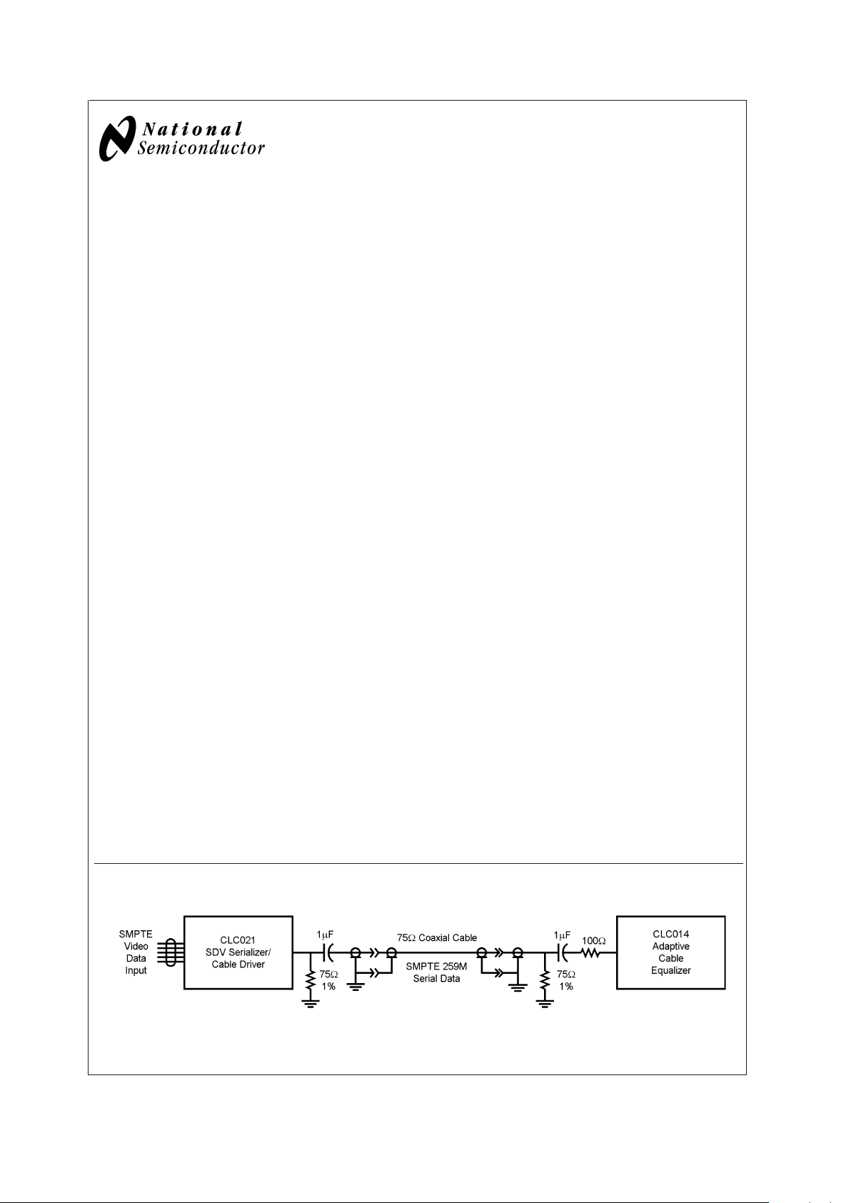
Typical Application
10136812
July 2003
CLC021 SMPTE 259M Digital Video Serializer with EDH Generation and Insertion
© 2003 National Semiconductor Corporation DS101368 www.national.com
Page 2
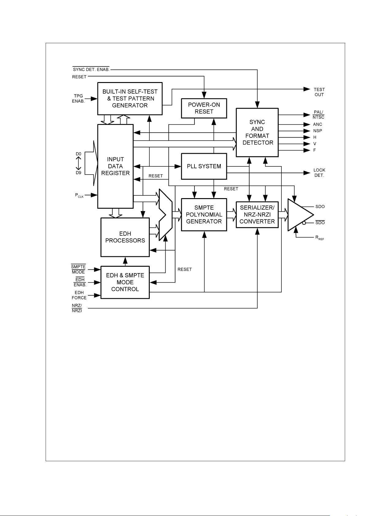
Block Diagram
10136801
CLC021
www.national.com 2
Page 3
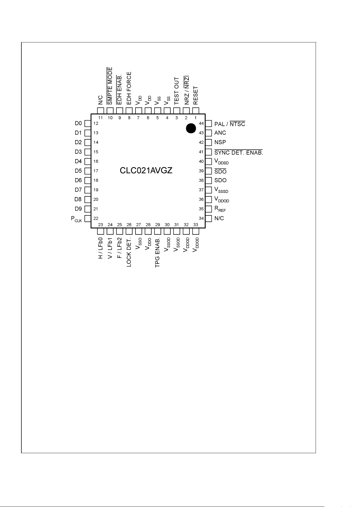
Connection Diagram
10136802
44-Pin Metric PQFP
Order Number CLC021AVGZ-5.0 or CLC021AVGZ-3.3
See NS Package Number VGZ44A
CLC021
www.national.com3
Page 4
Absolute Maximum Ratings (Note 1) It
is anticipated that this device will not be offered in a
military qualified version. If Military/Aerospace specified devices are required, please contact the National
Semiconductor Sales Office / Distributors for availability and specifications.
Supply Voltage (V
DD−VSS
):
CLC021AVGZ-5.0V 6.0V
CLC021AVGZ-3.3V 4.0V
CMOS/TTL Input Voltage (V
I
):
CLC021AVGZ-5.0V −0.5V to V
DD
+0.5V
CLC021AVGZ-3.3V -0.3V to V
DD
+0.3V
CMOS/TTL Output Voltage (V
O
):
CLC021AVGZ-5.0V −0.5V to V
DD
+0.5V
CLC021AVGZ-3.3V -0.3V to V
DD
+0.3V
CMOS/TTL Input Current (single input):
V
I=VSS
−0.5V: −5 mA
V
I=VDD
+0.5V: +5 mA
Input Current, Other Inputs:
±
1mA
CMOS/TTL Output Source/Sink Current:
±
16 mA
SDO Output Source Current: 22 mA
Package Thermal Resistance
θ
JA
44-lead Metric PQFP:
(
@
0 LFM airflow) 60˚C/W
(
@
500 LFM airflow) 43˚C/W
θ
JC
44-lead Metric PQFP: 17˚C/W
Storage Temp. Range: −65˚C to +150˚C
Junction Temperature: +150˚C
Lead Temperature (Soldering 4
Sec):
+260˚C
ESD Rating (HBM): 2 kV
ESD Rating (MM): 150V
Transistor Count: 33,400
Recommended Operating
Conditions
Supply Voltage (VDD−VSS):
CLC021AVGZ-5.0 5.0V
±
10%
CLC021AVGZ-3.3 3.3V
±
10%
CMOS/TTL Input Voltage: V
SS
to V
DD
Maximum DC Bias on SDO pins:
CLC021AVGZ-5.0 3.0V
±
10%
CLC021AVGZ-3.3 1.3V
±
10%
P
CLK
Frequency Range 10 to 40MHz
P
CLK
Duty Cycle 45 to 55%
D
N
and P
CLK
Rise/Fall Time 1.0 to 3.0 ns
Operating Free Air Temperature
(T
A
):
0˚C to +70˚C
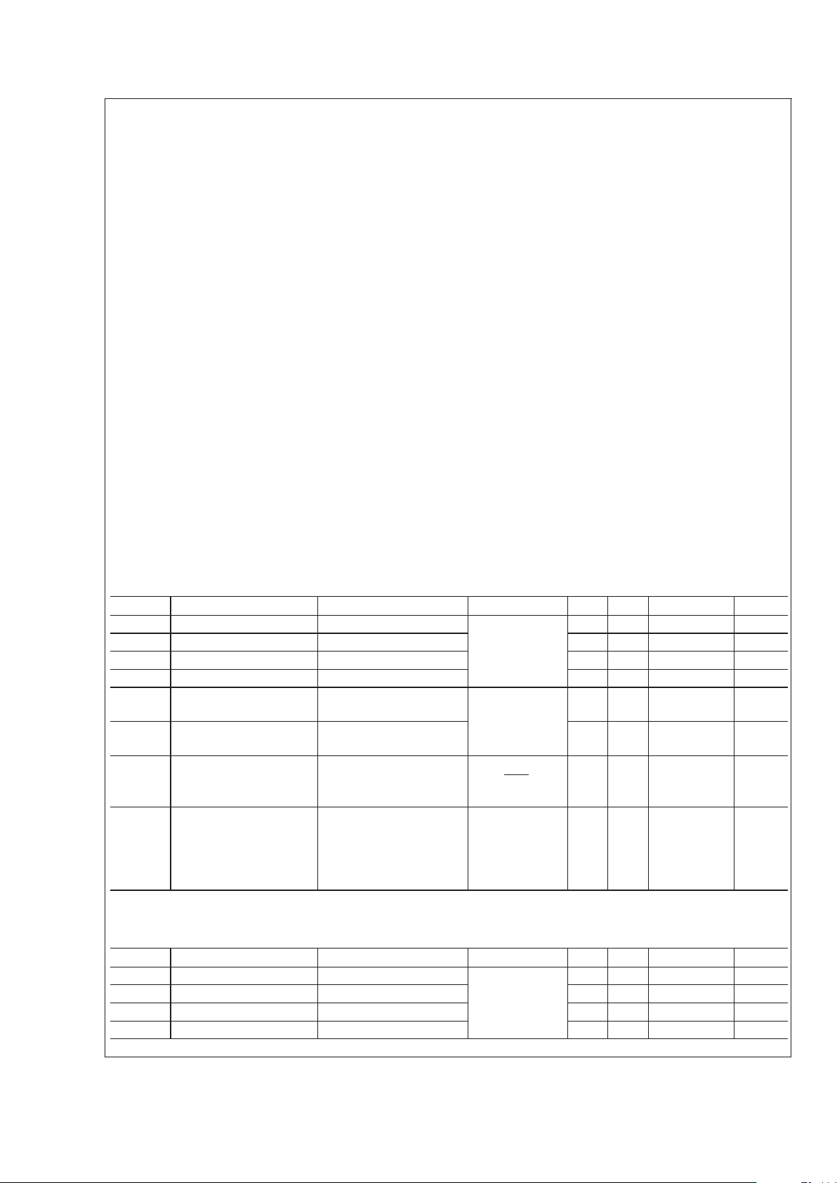
DC Electrical Characteristics—CLC021AVGZ-5.0
Over Supply Voltage and Operating Temperature ranges, unless otherwise specified (Notes 2, 3).
Symbol Parameter Conditions Reference Min Typ Max Units
V
IH
Input Voltage High Level
All CMOS Inputs
2.0 V
DD
V
V
IL
Input Voltage Low Level V
SS
0.8 V
I
IH
Input Current High Level VIH=V
DD
+40 +60 µA
I
IL
Input Current Low Level VIL=V
SS
-1 -20 µA
V
OH
CMOS Output Voltage
High Level
IOH= −10 mA
All CMOS
Outputs
2.4 4.7 V
DD
V
V
OL
CMOS Output Voltage
Low Level
IOL= +10 mA
0.0 0.3 V
SS
+ 0.5V V
V
SDO
Serial Driver Output
Voltage
RL=75Ω 1%,
R
REF
= 1.69 kΩ 1%,
Figure 2
SDO, SDO 700 800 900 mV
P-P
I
DD
Power Supply Current,
Total
RL=75Ω 1%,
R
REF
= 1.69 kΩ 1%,
P
CLK
= 27 MHz, NTSC
Colour Bar Pattern,
Figure 2
47 60 mA
DC Electrical Characteristics—CLC021AVGZ-3.3
Over Supply Voltage and Operating Temperature ranges, unless otherwise specified (Notes 2, 3).
Symbol Parameter Conditions Reference Min Typ Max Units
V
IH
Input Voltage High Level
All CMOS Inputs
2.0 V
DD
V
V
IL
Input Voltage Low Level V
SS
0.6 V
I
IH
Input Current High Level VIH=V
DD
+22 +60 µA
I
IL
Input Current Low Level VIL=V
SS
-1 -20 µA
CLC021
www.national.com 4
Page 5
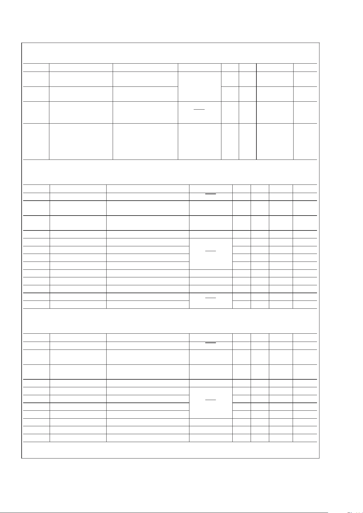
DC Electrical Characteristics—CLC021AVGZ-3.3 (Continued)
Over Supply Voltage and Operating Temperature ranges, unless otherwise specified (Notes 2, 3).
Symbol Parameter Conditions Reference Min Typ Max Units
V
OH
CMOS Output Voltage
High Level
IOH=−8mA
All CMOS
Outputs
2.4 3.0 V
DD
V
V
OL
CMOS Output Voltage
Low Level
IOL=+8mA
0.0 0.3 V
SS
+ 0.5V V
V
SDO
Serial Driver Output
Voltage
RL=75Ω 1%,
R
REF
= 1.69 kΩ 1%,
Figure 2
SDO, SDO 720 800 880 mV
P-P
I
DD
Power Supply Current,
Total
RL=75Ω 1%,
R
REF
= 1.69 kΩ 1%,
P
CLK
= 27 MHz, NTSC
Colour Bar Pattern,
Figure 2
33 55 mA
AC Electrical Characteristics—CLC021AVGZ-5.0
Over Supply Voltage and Operating Temperature ranges, unless otherwise specified (Note 3).
Symbol Parameter Conditions Reference Min Typ Max Units
BR
SDO
Serial Data Rate (Note 5) SDO, SDO 100 400 Mbps
F
P
CLK
Reference Clock
Input Frequency
P
CLK
10 40 MHz
Reference Clock Duty
Cycle
P
CLK
45 50 55 %
t
r,tf
Rise Time, Fall Time DN,P
CLK
1.0 1.5 3.0 ns
t
j
Serial Output Jitter 270 Mbps,Figure 2, (Note 6)
SDO, SDO
220 ps
P-P
t
jit
Serial Output Jitter (Notes 4, 5) 100 200 ps
P-P
tr,t
f
Rise Time, Fall Time 20%–80%, (Notes 4, 5) 500 800 1500 ps
Output Overshoot (Note 4) 1 %
t
LOCK
Lock Time (Notes 5, 7) 75 µs
t
SU
Setup Time Figure 3 (Note 4) DNto P
CLK
32 ns
t
HLD
Hold Time Figure 3 (Note 4) DNfrom P
CLK
32 ns
L
GEN
Output Inductance (Note 4)
SDO, SDO
6nH
R
GEN
Output Resistance (Note 4) 25k Ω
AC Electrical Characteristics—CLC021AVGZ-3.3
Over Supply Voltage and Operating Temperature ranges, unless otherwise specified (Note 3).
Symbol Parameter Conditions Reference Min Typ Max Units
BR
SDO
Serial Data Rate (Note 5) SDO, SDO 100 400 Mbps
F
P
CLK
Reference Clock
Input Frequency
P
CLK
10 40 MHz
Reference Clock Duty
Cycle
P
CLK
45 50 55 %
t
r,tf
Rise Time, Fall Time DN,P
CLK
1.0 1.5 3.0 ns
t
j
Serial Output Jitter 270 Mbps,Figure 2, (Note 6)
SDO, SDO
220 ps
P-P
t
jit
Serial Output Jitter (Notes 4, 5) 100 200 ps
P-P
tr,t
f
Rise Time, Fall Time 20%–80%, (Notes 4, 5) 500 800 1500 ps
Output Overshoot (Note 4) 1 %
t
LOCK
Lock Time (Notes 5, 7) 75 µs
t
SU
Setup Time Figure 3 (Note 4) DNto P
CLK
42 ns
t
HLD
Hold Time Figure 3 (Note 4) DNfrom P
CLK
42 ns
CLC021
www.national.com5
Page 6
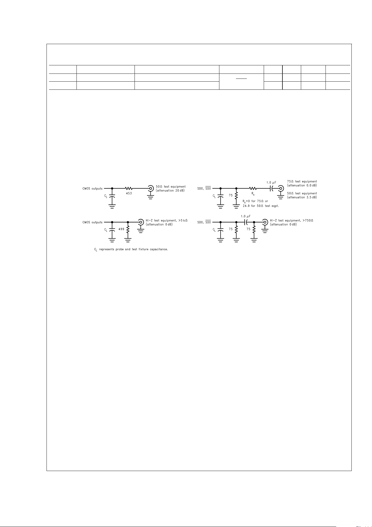
AC Electrical Characteristics—CLC021AVGZ-3.3 (Continued)
Over Supply Voltage and Operating Temperature ranges, unless otherwise specified (Note 3).
Symbol Parameter Conditions Reference Min Typ Max Units
L
GEN
Output Inductance (Note 4)
SDO, SDO
6nH
R
GEN
Output Resistance (Note 4) 25k Ω
Note 1: “Absolute Maximum Ratings” are those parameter values beyond which the life and operation of the device cannot be guaranteed. The stating herein of
these maximums shall not be construed to imply that the device can or should be operated at or beyond these values. The table of “Electrical Characteristics”
specifies acceptable device operating conditions.
Note 2: Current flow into device pins is defined as positive. Current flow out of device pins is defined as negative. All voltages are stated referenced to V
SS
=0V.
Note 3: Typical values are stated for V
DD
= +5.0V (CLC021AVGZ-5.0) or +3.3V (CLC021AVGZ-3.3) and TA= +25˚C.
Note 4: Specification is guaranteed by design.
Note 5: R
L
=75Ω, AC-coupled@270 M
bps,RREF
= 1.69 kΩ 1%, See Test Loads and Figure 2.
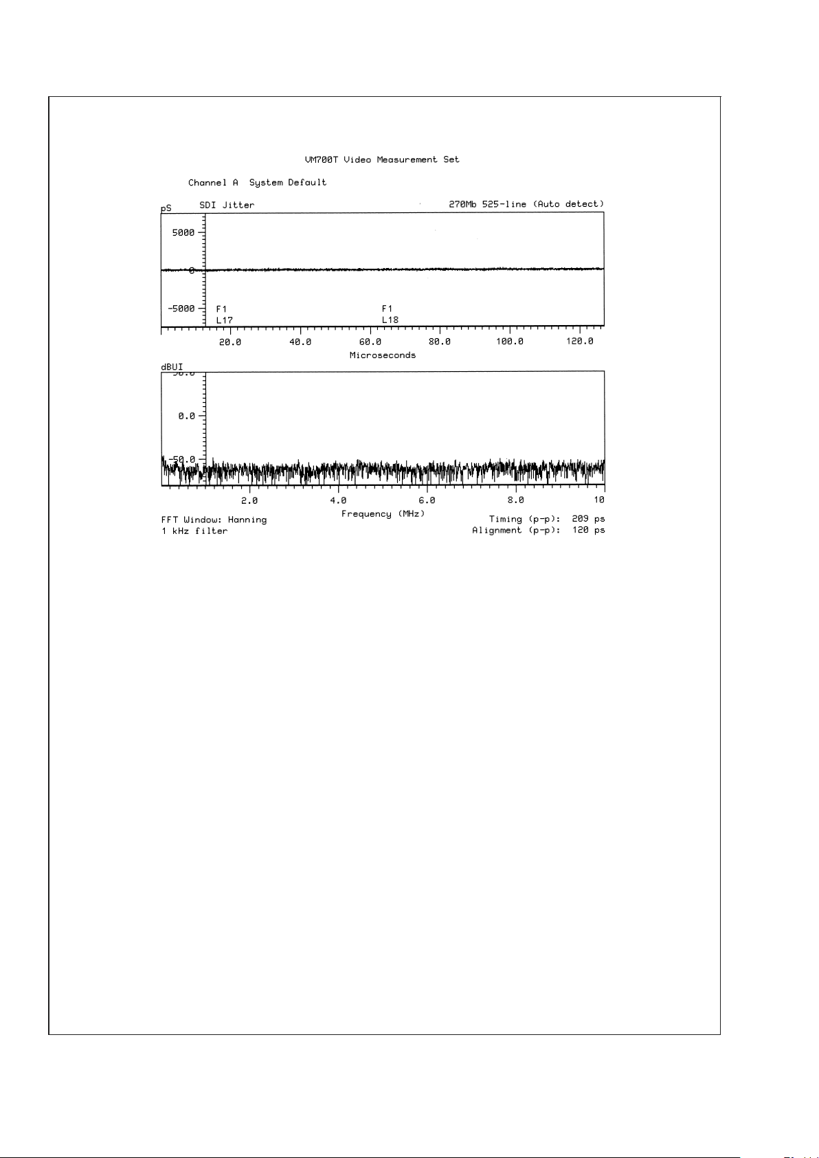
Note 6: CLC021 mounted in the SD021EVK board, configured in BIST mode (NTSC colour bars) with P
CLK
= 27 MHz derived from Tektronix TG2000 black-burst
reference. Timing jitter measured with Tektronix VM700T using jitter measurement FFT mode, frame rate, 1 kHz filter bandwidth, Hanning window.
Note 7: Measured from rising-edge of first P
CLK
cycle until Lock Detect output goes high (true).
Test Loads
10136803
FIGURE 1. Test Loads
CLC021
www.national.com 6
Page 7

Test Loads (Continued)
10136804
FIGURE 2. Test Circuit
CLC021
www.national.com7
Page 8
Timing Diagram
Device Operation
The CLC021 SMPTE 259M Serial Digital Video Serializer is
used in digital video signal origination equipment: cameras,
video tape recorders, telecines and video test and other
equipment. It converts parallel component or composite digital video signals into serial format. Logic levels within this
equipment are normally TTL-compatible as produced by
CMOS or bipolar logic devices. The encoder produces ECLcompatible serial digital video (SDV) signals conforming to
SMPTE 259M-1997. The CLC021 operates at all standard
SMPTE and ITU-R parallel data rates. In addition, the
CLC021 can serialize other 8- and 10-bit data.
VIDEO DATA PROCESSING CIRCUITS
The input data register accepts 8- or 10-bit parallel data
and clock signals having HCMOS/LSTTL-compatible signal
levels. Parallel data may conform to any of several standards: SMPTE 125M, SMPTE 267M, SMPTE 244M or
ITU-R BT.601. If the data is 8-bit, it is converted to a 10-bit
representation according to the type of data being input:
component 4:2:2 per SMPTE 259M paragraph 7.1.1, composite NTSC per paragraph 8.1.1 or composite PAL per
paragraph 9.1.1. Eight-bit video data corresponds to the
upper 8 bits of the 10-bit video data word and is MSBaligned. Output from this register feeds the TRS (sync)
character detector, SMPTE polynomial generator/serializer
and the EDH polynomial generators/serializers and control
system. All parallel data and clock inputs have internal pulldown devices.
The sync detector or TRS character detector receives data
from the input register. The detection function is controlled
by Sync Detect Enable, a low-true, TTL-compatible, external
signal. Synchronization words, the timing reference signals
(TRS), start-of-active-video (SAV) and end-of-active-video
(EAV) are defined in SMPTE 125M and 244M. The sync
detector supplies control signals to the SMPTE polynomial
generator to identify the presence of valid video data, and to
the EDH control block. In SMPTE mode, TRS character
LSB-clipping as prescribed in ITU-R BT.601 is enabled. LSBclipping causes all TRS characters with a value between
000h and 003h to be forced to 000h and all TRS characters
with a value between 3FCh and 3FFh to be forced to 3FFh.
Clipping is done prior to encoding or EDH character generation. This function is disabled in non-SMPTE mode operation.
Outputs from the sync detector are:
1. H, V, and F or Line/Field ID — For component video,
these are registered outputs corresponding to input TRS
data bits 6, 7 and 8, respectively. These outputs are
disabled in non-SMPTE mode. The outputs are active
HIGH-true. For composite video, these outputs correspond to the line and field ID encoded as input parallel
data bits 2 (MSB) through 0. These outputs are registered for the duration of the applicable field.
2. NSP — New Sync Position: A function and output indicating that a new or out-of-place TRS character has
been detected. This output remains active for at least
one horizontal line period (reset by EAV) or unless reactivated by a subsequent new or out-of-place TRS.
Activation of this function flushes the existing state of the
machine reseting the EDH generator, SMPTE polynomial generator, serializer and NRZ-NRZI converter. This
function is disabled in non-SMPTE mode operation. The
output is active HIGH-true.
3. ANC — Ancilliary data location output: Indicates that the
ancilliary data header (component) or flag (composite)
has been detected. The output is a pulse having a
duration of one P
CLK
period. The output is active HIGH-
true.
SMPTE POLYNOMIAL GENERATOR AND CONTROLS
The SMPTE Mode input allows the CLC021 to function both
as a full SMPTE 259M encoder or general-purpose 8- or
10-bit serializer. SMPTE mode is enabled when this input is
LOW. Non-SMPTE mode is enabled when this pin is HIGH.
This pin is pulled internally to V
SS
when unconnected. When
in SMPTE mode, the SMPTE polynomial generator; TRS
sync detection circuitry; EDH control circuitry; H, V, F and
NSP outputs and TRS clipping are enabled.
The SMPTE polynomial generator accepts the parallel
video data and encodes it using the polynomial X
9+X4
+1
as specified in SMPTE 259M (1997 rev.), paragraph 5 and
Annex C. The transmission bit order is LSB-first, per paragraph 6.
10136805
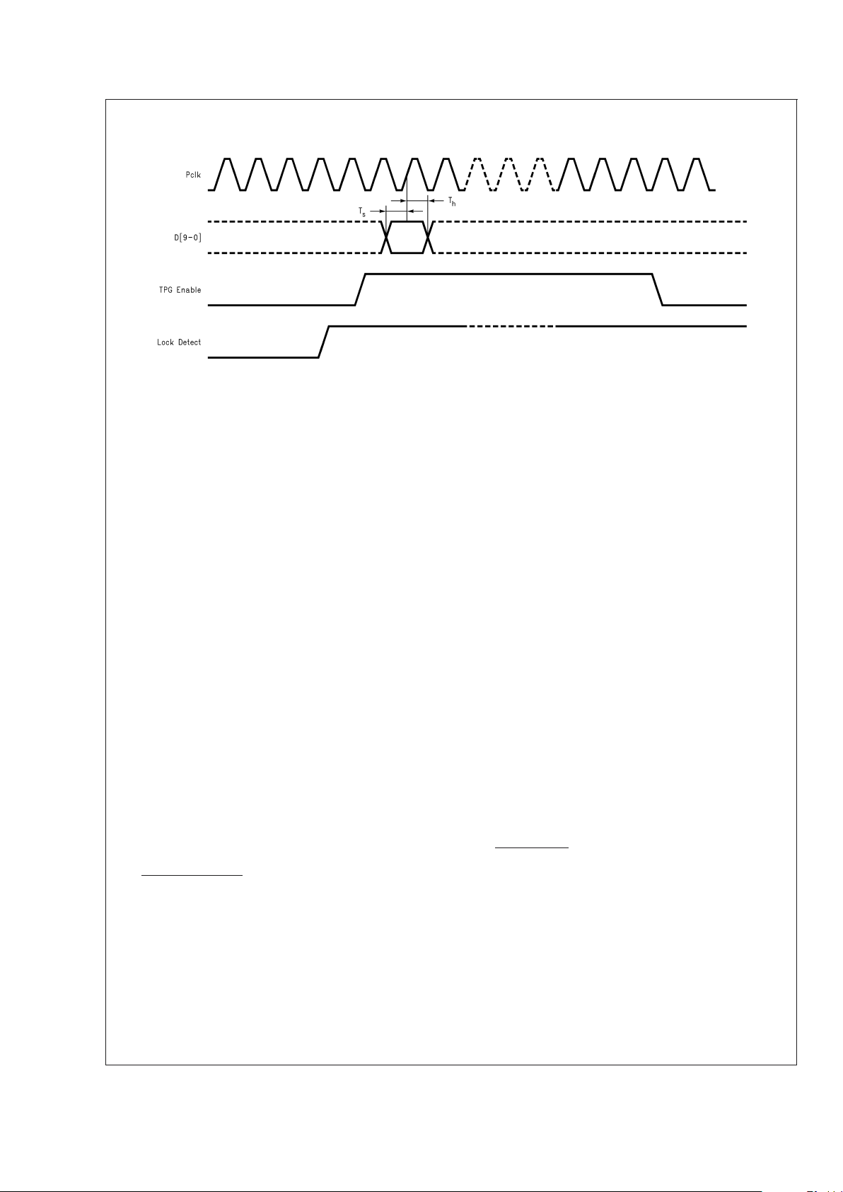
FIGURE 3. Setup and Hold Timing
CLC021
www.national.com 8
Page 9

Device Operation (Continued)
NRZ-TO-NRZI CONVERTER
The NRZ-to-NRZI converter accepts NRZ serial data from
the SMPTE and EDH polynomial genertors and converts it to
NRZI using the polynomial (X + 1) per SMPTE 259M, paragraph 5.2 and Annex C. The converter’s output goes to the
output buffer amplifier. The NRZ/NRZI input enables this
conversion function. Conversion from NRZ to NRZI is enabled when the input is a logic LOW. Conversion to NRZI is
disabled when this input is a logic-HIGH. This function is not
affected by the SMPTE mode control input. The input pin is
pulled internally to V
SS
(NRZI enabled) when unconnected.
EDH SYSTEM OPERATION
The CLC021 has EDH character and flag generation and
insertion circuitry which operates as proposed in SMPTE
RP-165. Inputs and circuitry are provided to control generation and automatic insertion of the EDH check words at
proper locations in the serial data output.
The EDH polynomial generators accept parallel data from
the input register and generate 16-bit serial check words
using the polynomial X
16+X12+X6
+ 1. Separate calculations are made for each video field prior to serialization.
Separate CRCs for the full-field and active picture along with
status flags are inserted and serially transmitted with the
other data. Upon being reset, the initial state of all EDH
check characters is 00h.
The EDH control system accepts input from the sync detector and controls the EDH polynomial generator and SMPTE/
EDH polynomial insertion multiplexer. EDH Enable,anexternal TTL-compatible, low-true input, enables this circuitry.
The controller inserts the EDH check words in the serial data
stream at the correct positions in the ancilliary data space
per SMPTE 259M paragraph 7.3, 8.4.4 or 9.4.4 and per
SMPTE RP-165. Ancilliary data space is formatted per
SMPTE 291M.
The EDH Force control input causes the insertion of new
EDH checkwords and flags into the serial output regardless
of the previous condition of EDH checkwords and flags in the
input parallel data. This function may be used in situations
where video content has been editted thus making the previous EDH information invalid.
The NTSC/PAL output indicates the type of component or
composite data standard being input to the CLC021. This
output is useful for troubleshooting or may be used to drive a
panel indicator. The output is high when 625-line PAL data is
being input and low when 525-line NTSC data is being input.
PHASE-LOCKED LOOP AND VCO
The phase-locked loop (PLL) system generates the output
serial data clock at 10x the parallel data clock frequency.
This system consists of a VCO, divider chain, phasefrequency detector and internal loop filter. The VCO free-
running frequency is internally set. The PLL automatically
generates the appropriate frequency for the serial clock rate
using the parallel data clock (P
CLK
) frequency as its reference. Loop filtering is internal to the CLC021. The VCO halts
when no P
CLK
signal is present or is inactive. P
CLK
should be
applied after power to the device.
The VCO has separate V
SSO
and V
DDO
power supply feeds,
pins 27 and 28, which may be supplied power via an external
low-pass filter, if desired. The PLL acquisition (lock) time is
less than 75 µs
@
270 Mbps.
LOCK DETECT
The lock detect output (pin 26) of the phase-frequency detector is a logic HIGH when the loop is locked. The output is
CMOS/TTL-compatible and is suitable for driving other
CMOS devices or an LED indicator. The Lock Detect pin
reports the status of the PLL. When P
CLK
is lost, it will switch
low at the event.
SERIAL DATA OUTPUT BUFFER
The current-mode serial data outputs provide low-skew
complimentary or differential signals. The output buffer design can drive 75Ω coaxial cables (AC-coupled) or 10K/100K
ECL/PECL-compatible devices (DC-coupled). Output levels
are 800 mV
P-P
±
10% into 75Ω AC-coupled, back-matched
loads. The output level is 400 mV
P-P
±
10% when DCcoupled into 75Ω. (See Application Information for details.)
The 75Ω resistors connected to the SDO outputs are backmatching resistors. No series back-matching resistors
should be used. Output level is controlled by the value of
R
REF
connected to pin 35. The value of R
REF
is normally
1.69 kΩ,
±
1%. The output buffer is static when the device is
in an out-of-lock condition. Separate V
SSSD
and V
DDSD
power feeds, pins, 37 and 40 are provided for the serial
output driver.
POWER-ON RESET AND RESET INPUT
The CLC021 has an internally controlled, automatic, power-
on-reset circuit. Reset clears TRS detection circuitry, all
latches, registers, counters and polynomial generators, sets
the EDH characters to 00h and disables the serial output.
The SDO outputs are tri-stated during power-on reset. The
part will remain in the reset condition until the parallel input
clock is applied.
An active-HIGH-true, manual reset input is available at
pin 1. It resets both the digital and PLL blocks. The reset
input has an internal pull-down device and is inactive when
unconnected.
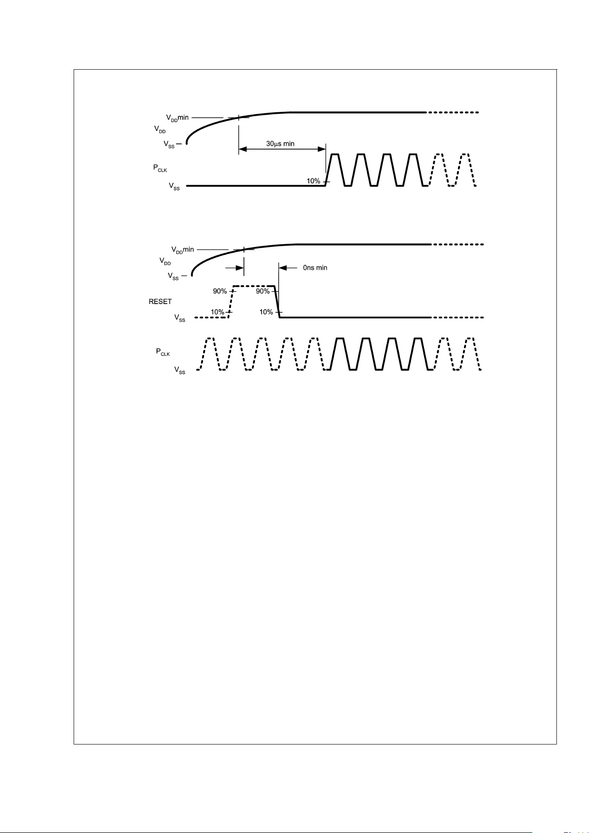
It is recommended that P
CLK
not be asserted until at least
30 µs after power has reached V
DD
min. See Figure 4.If
manual reset is used during power-on, then P
CLK
may be
asserted at any time as long as manual reset is not deasserted until V
DD
min is reached. See Figure 5.
CLC021
www.national.com9
Page 10
Device Operation (Continued)
BUILT-IN SELF-TEST (BIST)
The CLC021 has a built-in self-test (BIST) function. The
BIST performs a comprehensive go/no-go test of the device.
The test uses either a full-field colour bar for NTSC or a PLL
pathological for PAL as the test data pattern. Data is input
internally in the input data register, processed through the
device and tested for errors. A go/no-go indication is given at
the Test_Output. Table 1 gives device pin functions and
Table 2 gives the test pattern codes used for this function.
The signal level at Test_Output, pin 3, indicates a pass or fail
condition.
The BIST is initiated by applying the code for the desired
BIST to D0 through D3 (D9 through D4 are 00h) and a 27
MHz clock at the P
CLK
input. Since all parallel data inputs are
equipped with an internal pull-down device, only those inputs
D0 through D3 which require a logic-1 need be pulled high.
After the Lock_Detect output goes high indicating the VCO is
locked on frequency, TPG_Enable, pin 29, is taken to a logic
high. The Lock_Detect output may be temporarily connected
to TPG_Enable to automate BIST operation. Test_Output,
pin 3, is monitored for a pass/fail indication. If no errors have
been detected, this output will go to a logic high level approximately 2 field intervals after TPG_Enable is taken high.
If errors have been detected in the internal circuitry of the
CLC021, Test_Output will remain low until the test is terminated. The BIST is terminated by taking TPG _Enable to a
logic low. Continuous serial data output is available during
the test.
10136815
FIGURE 4. Power-On Reset Sequence
10136814
FIGURE 5. Power-On Reset Sequence with Manual Reset
CLC021
www.national.com 10
Page 11

Device Operation (Continued)
TEST PATTERN GENERATOR
The CLC021 includes an on-board test pattern generator
(TPG). Four full-field component video test patterns for both
NTSC and PAL standards, and 4x3 and 16x9 raster sizes are
produced. The test patterns are: flat-field black, PLL pathological, equalizer (EQ) pathological and a modified 75%,
8-colour vertical bar pattern. The pathologicals follow recommendations contained in SMPTE RP 178 – 1996 regarding
the test data used. The colour bar pattern does not incorporate bandwidth limiting coding in the chroma and luma data
when transitioning between the bars. For this reason, it may
not be suitable for use as a visual test pattern or for input to
video D-to-A conversion devices unless measures are taken
to restrict the production of out-of-band frequency components.
The TPG is operated by applying the code for the desired
test pattern to D0 through D3 (D4 through D9 are 00h). Since
all parallel data inputs are equipped with internal pull-down
devices, only those inputs D0 through D3 which require a
logic-1 need be pulled high. Next, apply a 27 MHz or 36 MHz
signal, appropriate to the raster size desired, at the P
CLK
input and wait until the Lock_Detect output goes true indicating the VCO is locked on frequency. Then, take
TPG_Enable, pin 29, to a logic high. The serial test pattern
data appears on the SDO outputs. The Lock_Detect output
may be temporarily connected to TPG_Enable to automate
TPG operation. The TPG mode is exited by taking TPG_Enable to a logic low. Table 1 gives device pin functions for this
mode. Table 2 gives the available test patterns and selection
codes.
10136806
FIGURE 6. Built-In Self-Test Control Sequence
10136807
FIGURE 7. Test Pattern Generator Control Sequence
CLC021
www.national.com11
Page 12

Device Operation (Continued)
TABLE 1. BIST and Test Pattern Generator Control Functions
Pin Name Function
12 D0 TPG Code Input LSB
13 D1 TPG Code Input
14 D2 TPG Code Input
15 D3 TPG Code Input MSB
29 TPG_EN TPG Enable, Active High True
3 Test_Out BIST Pass/Fail Output. Pass=High
(See text for Timing Requirements)
TABLE 2. Component Video Test Pattern Selection
Standard Frame Test Pattern D3 D2 D1 D0
NTSC 4x3 Flat-Field Black 0 0 0 0
NTSC 4x3 PLL Pathological 0 0 0 1
NTSC 4x3 EQ Pathological 0 0 1 0
NTSC 4x3 Colour Bars, 75%, 8-Bars (modified, see text), BIST 0 0 1 1
PAL 4x3 Flat-Field Black 0 1 0 0
PAL 4x3 PLL Pathological, BIST 0 1 0 1
PAL 4x3 EQ Pathological 0 1 1 0
PAL 4x3 Colour Bars, 75%, 8-Bars (modified, see text) 0 1 1 1
NTSC 16x9 Flat-Field Black 1 0 0 0
NTSC 16x9 PLL Pathological 1 0 0 1
NTSC 16x9 EQ Pathological 1 0 1 0
NTSC 16x9 Colour Bars, 75%, 8-bars (modified, see text) 1 0 1 1
PAL 16x9 Flat-Field Black 1 1 0 0
PAL 16x9 PLL Pathological 1 1 0 1
PAL 16x9 EQ Pathological 1 1 1 0
PAL 16x9 Colour Bars, 75%, 8-Bars (modified, see text) 1 1 1 1
Note: D9 through D4 = 0 (binary)
CLC021
www.national.com 12
Page 13

Pin Descriptions
Pin Name Description
1 Reset Manual Reset Input (High True)
2 NRZ-NRZI
NRZ-to-NRZI Conversion Control (NRZ=High, NRZI=Low)
3 Test Out Test Out (BIST Pass/Fail Indicator)
4V
SS
Negative Power Supply Input (Digital Logic)
5V
SS
Negative Power Supply Input (Digital Logic)
6V
DD
Positive Power Supply Input (Digital Logic)
7V
DD
Positive Power Supply Input (Digital Logic)
8 EDH Force Force Insertion of New EDH and Flags in Serial Output Data (High True)
9 EDH Enable
EDH Enable Input (Low True)
10 SMPTE Mode
SMPTE/non-SMPTE Mode Select Input (SMPTE Mode=Low)
11 N/C No Connect
12 D0 Parallel Data Input (Internal Pull-Down to V
SS
)
13 D1 Parallel Data Input (Internal Pull-Down to V
SS
)
14 D2 Parallel Data Input (Internal Pull-Down to V
SS
)
15 D3 Parallel Data Input (Internal Pull-Down to V
SS
)
16 D4 Parallel Data Input (Internal Pull-Down to V
SS
)
17 D5 Parallel Data Input (Internal Pull-Down to V
SS
)
18 D6 Parallel Data Input (Internal Pull-Down to V
SS
)
19 D7 Parallel Data Input (Internal Pull-Down to V
SS
)
20 D8 Parallel Data Input (Internal Pull-Down to V
SS
)
21 D9 Parallel Data Input (Internal Pull-Down to V
SS
)
22 P
CLK
Parallel Clock Input (Internal Pull-Down to VSS)
23 H/Line-Field b0 (LSB) H-Bit Output (Component); Line-Field ID (Composite)
24 V/Line-Field b1 V-Bit Output (Component); Line-Field ID (Composite)
25 F/Line-Field b2 (MSB) F-Bit Output (Component); Line-Field ID (Composite)
26 Lock Detect Lock Detector Output (High True)
27 V
SSO
Negative Power Supply Input (PLL Supply)
28 V
DDO
Positive Power Supply Input (PLL Supply)
29 TPG Enable TPG Enable (High True)
30 V
SSOD
Negative Power Supply Input (PLL Digital Supply)
31 V
SSOD
Negative Power Supply Input (PLL Digital Supply)
32 V
DDOD
Positive Power Supply Input (PLL Digital Supply)
33 V
DDOD
Positive Power Supply Input (PLL Digital Supply)
34 N/C No Connect
35 R
REF
Output Level Reference Resistor (1.69 kΩ, 1% Nominal Value)
36 V
DDOD
Positive Power Supply Input (PLL Digital Supply)
37 V
SSSD
Negative Power Supply Input (Output Driver)
38 SDO Serial Data True Output
39 SDO
Serial Data Complement Output
40 V
DDSD
Positive Power Supply Input (Output Driver)
41 Sync Detect Enable
Parallel Data Sync Detection Enable Input (Low True)
42 NSP New Sync Position Output
43 ANC Ancilliary Data Header Flag Output
44 NTSC/PAL
NTSC/PAL Mode Indicator Output (PAL=High, NTSC=Low)
Note: All CMOS/TTL inputs have internal pull-down devices.
CLC021
www.national.com13
Page 14

Application Information
A typical application circuit for the CLC021 is shown in
Figure 8. This circuit demonstrates the capabilities of the
CLC021 and allows its evaluation in a variety of configurations. Assembled demonstration boards with more comprehensive evaluation options are available, part number
SD021-5EVK (5V device) or SD021-3EVK (3.3V device).
The boards may be ordered through any of National’s sales
offices. Complete circuit board layouts and schematics including Gerber photoplot files, for the demonstration boards
are available on National’s WEB site in the application information for this device. For latest information, please see:
www.national.com/appinfo/interface.
APPLICATION CIRCUIT
The SD021EVK application circuit boards, Figure 9, can
accommodate different input and output drive and loading
options. Pin headers are provided for input and control I/O
signal access. Install the appropriate value resistor packs,
220Ω at RP1 and RP3 and 330Ω at RP2 and RP4, for TTL
cabled interfaces before applying input signals. Install 51Ω
resistor packs at RP2 and RP4 for signal sources requiring
such loading. Remove any resistor packs at RP1 and RP3
when using 50Ω source loading.
The board’s outputs may be DC interfaced to PECL inputs by
first installing 124Ω resistors at R1B and R2B, changing R1A
and R2A to 187Ω and replacing C1 and C2 with short
circuits. The PECL inputs should be directly connected to J1
and J2 without cabling. If 75Ω cabling is used to connect the
CLC021 to the PECL inputs, the voltage dividers used on the
CLC021 outputs must be removed and re-installed on the
circuit board where the PECL device is mounted. This will
provide correct termination for the cable and biasing for both
the CLC021’s outputs and the PECL inputs. It is most important to note that a 75Ω or equivalent DC loading (measured
with respect to the negative supply rail) must always be
installed at both of the CLC021’s SDO outputs to obtain
proper signal levels from device. When using 75Ω Theveninequivalent load circuits, the DC bias applied to the SDO
outputs should not exceed +3V (+1.3V for CLC021AVGZ-
3.3) with respect to the negative supply rail. Serial output
levels should be reduced to 400 mV
p-p
by changing R
REF
to
3.4 kΩ. This may be done by removing the Output Level
shorting jumper on the post header.
10136808
FIGURE 8. Typical Application Circuit
CLC021
www.national.com 14
Page 15

Application Information (Continued)
The Test Out output is intended for monitoring by equipment
having high impedance test loading (
>
500Ω). If the Lock
Detect output is to be externally monitored, the attached
monitoring circuit should present a DC resistance greater
than 5 kΩ so as not to affect Lock Detect indicator operation.
MEASURING JITTER
The test method used to obtain the timing jitter value given in
the AC Electrical Specification table is based on procedures
and equipment described in SMPTE RP 192-1996. The recommended practice discusses several methods and indicator devices. An FFT method performed by standard video
test equipment was used to obtain the data given in this data
sheet. As such, the jitter characteristics (or jitter floor) of the
measurement equipment, particularly the measurement analyzer, become integral to the resulting jitter value. The
method and equipment were chosen so that the test can be
easily duplicated by the design engineer using most standard digital video test equipment. In so doing, similar results
should be achieved. The intrinsic jitter floor of the CLC021’s
PLL is approximately 25% of the typical jitter given in the
electrical specifications. In production, device jitter is measured on automatic IC test equipment (ATE) using a different
method compatible with that equipment. Jitter measured
using this ATE yields values approximately 50% of those
obtained using the video test equipment.
10136809
Connect LOCK DETECT to TPG ENABLE for test pattern generator function.
Remove RP1 & RP3 and replace RP2 & RP4 with 50Ω resistor packs for coax interfacing.
Install RP1-4 when using ribbon cable for input interfacing.
This board is designed for use with TTL power supplies only.
FIGURE 9. SD021EVK Schematic Diagram
CLC021
www.national.com15
Page 16
Application Information (Continued)
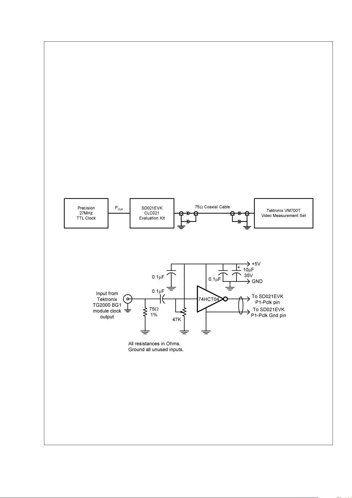
The jitter test setup used to obtain values quoted in the data
sheet consists of:
•
National Semiconductor SD021-5EVK (SD021-3EVK),
CLC021 evaluation kit
•
Tektronix TG2000 signal generation platform with DVG1
option
•
Tektronix VM700T Option 1S Video Measurement Set
•
Tektronix TDS 794D, Option C2 oscilloscope
•
Tektronix P6339A passive probe
•
75Ω coaxial cable, 3 ft., Belden 8281 or RG59 (2 required)
•
ECL-to-TTL/CMOS level converter/amplifier, (see
Figure 11).
Apply the black-burst reference clock from the TG2000 signal generator’s BG1 module 27 MHz clock output to the level
converter input. The clock amplitude converter schematic is
shown in Figure 11. Adjust the input bias control to give a
50% duty cycle output as measured on the oscilloscope/
probe system. Connect the level translator to the SD021EVK
board, connector P1, P
CLK
pins (the outer-most row of pins
is ground). Configure the SD021EVK to operate in the NTSC
colour bars, BIST mode. Configure the VM700T to make the
jitter measurement in the jitter FFT mode at the frame rate
with 1 kHz filter bandwidth and Hanning window. Configure
the setup as shown in Figure 10. Switch the test equipment
on (from standby mode) and allow all equipment temperatures stabilize per manufacturer’s recommendation. Measure the jitter value after allowing the instrument’s reading to
stabilize (about 1 minute). Consult the VM700T Video Measurement Set Option 1S Serial Digital Measurements User
Manual (document number 071-0074-00) for details of
equipment operation.
The VM700T measurement system’s jitter floor specification
at 270 Mbps is given as 200 ps
±
20% (100 ps±5% typical)
of actual components from 50 Hz to 1 MHz and 200 ps
+60%, -30% of actual components from 1 MHz to 10 MHz.
To obtain the actual residual jitter of the CLC021, a root-sumsquare adjustment of the jitter reading must be made to
compensate for the measurement system’s jitter floor specification. For example, if the jitter reading is 250 ps, the
CLC021 residual jitter is the square root of (250
2
− 2002)=
150 ps. The accuracy limits of the reading as given above
apply.
10136810
FIGURE 10. Jitter Test Circuit
10136813
FIGURE 11. ECL-to-TTL/CMOS Level Converter/Amplifer
CLC021
www.national.com 16
Page 17
Application Information (Continued)
PCB LAYOUT AND POWER SYSTEM BYPASS
RECOMMENDATIONS
Circuit board layout and stack-up for the CLC021 should be
designed to provide noise-free power to the device. Good
layout practice also will separate high frequency or high level
inputs and outputs to minimize unwanted stray noise pickup,
feedback and interference. Power system performance may
be greatly improved by using thin dielectrics (4 to 10 mils) for
power/ground sandwiches. This increases the intrinsic capacitance of the PCB power system which improves power
supply filtering, especially at high frequencies, and makes
the value and placement of external bypass capacitors less
critical. External bypass capacitors should include both RF
ceramic and tantalum electrolytic types. RF capacitors may
use values in the range 0.01 µF to 0.1 µF. Tantalum capacitors may be in the range 2.2 µF to 10 µF. Voltage rating for
tantalum capacitors should be at least 5X the power supply
voltage being used. It is recommended practice to use two
vias at each power pin of the CLC021 as well as all RF
bypass capacitor terminals. Dual vias reduce the interconnect inductance by up to half, thereby reducing interconnect
inductance and extending the effective frequency range of
the bypass components.
The outer layers of the PCB may be flooded with additional
V
SS
(ground) plane. These planes will improve shielding and
isolation as well as increase the intrinsic capacitance of the
power supply plane system. Naturally, to be effective, these
planes must be tied to the V
SS
power supply plane at frequent intervals with vias. Frequent via placement also improves signal integrity on signal transmission lines by providing short paths for image currents which reduces signal
distortion. The planes should be pulled back from all transmission lines and component mounting pads a distance
equal to the width of the widest transmission line or the
thickness of the dielectric separating the transmission line
from the internal power or ground plane(s) whichever is
greater. Doing so minimizes effects on transmission line
impedances and reduces unwanted parasitic capacitances
at component mounting pads.
In especially noisy power supply environments, such as is
often the case when using switching power supplies, separate filtering may be used at the CLC021’s VCO and output
driver power pins. The CLC021 was designed for this situation. The digital section, VCO and output driver power supply
feeds are independent (see pinout description table and
pinout drawing for details). Supply filtering may take the form
of L-section or pi-section, L-C filters in series with these V
DD
inputs. Such filters are available in a single package from
several manufacturers. Despite being independent feeds, all
device power supplies should be applied simultaneously as
from a common source. The CLC021 is free from power
supply latch-up caused by circuit-induced delays between
the device’s three separate power feed systems.
10136811
FIGURE 12. Jitter Plots
CLC021
www.national.com17
Page 18

Physical Dimensions inches (millimeters) unless otherwise noted
44-Pin Metric PQFP
Order Number CLC021AVGZ-5.0 or CLC21AVGZ-3.3
NS Package Number VGZ44A
LIFE SUPPORT POLICY
NATIONAL’S PRODUCTS ARE NOT AUTHORIZED FOR USE AS CRITICAL COMPONENTS IN LIFE SUPPORT
DEVICES OR SYSTEMS WITHOUT THE EXPRESS WRITTEN APPROVAL OF THE PRESIDENT AND GENERAL
COUNSEL OF NATIONAL SEMICONDUCTOR CORPORATION. As used herein:
1. Life support devices or systems are devices or
systems which, (a) are intended for surgical implant
into the body, or (b) support or sustain life, and
whose failure to perform when properly used in
accordance with instructions for use provided in the
labeling, can be reasonably expected to result in a
significant injury to the user.
2. A critical component is any component of a life
support device or system whose failure to perform
can be reasonably expected to cause the failure of
the life support device or system, or to affect its
safety or effectiveness.
National Semiconductor
Americas Customer
Support Center
Email: [email protected]
Tel: 1-800-272-9959
National Semiconductor
Europe Customer Support Center
Fax: +49 (0) 180-530 85 86
Email: [email protected]
Deutsch Tel: +49 (0) 69 9508 6208
English Tel: +44 (0) 870 24 0 2171
Français Tel: +33 (0) 1 41 91 8790
National Semiconductor
Asia Pacific Customer
Support Center
Email: [email protected]
National Semiconductor
Japan Customer Support Center
Fax: 81-3-5639-7507
Email: [email protected]
Tel: 81-3-5639-7560
www.national.com
CLC021 SMPTE 259M Digital Video Serializer with EDH Generation and Insertion
National does not assume any responsibility for use of any circuitry described, no circuit patent licenses are implied and National reserves the right at any time without notice to change said circuitry and specifications.
 Loading...