

Page 1
CLC018
8 x 8 Digital Crosspoint Switch, 1.4 Gbps
General Description
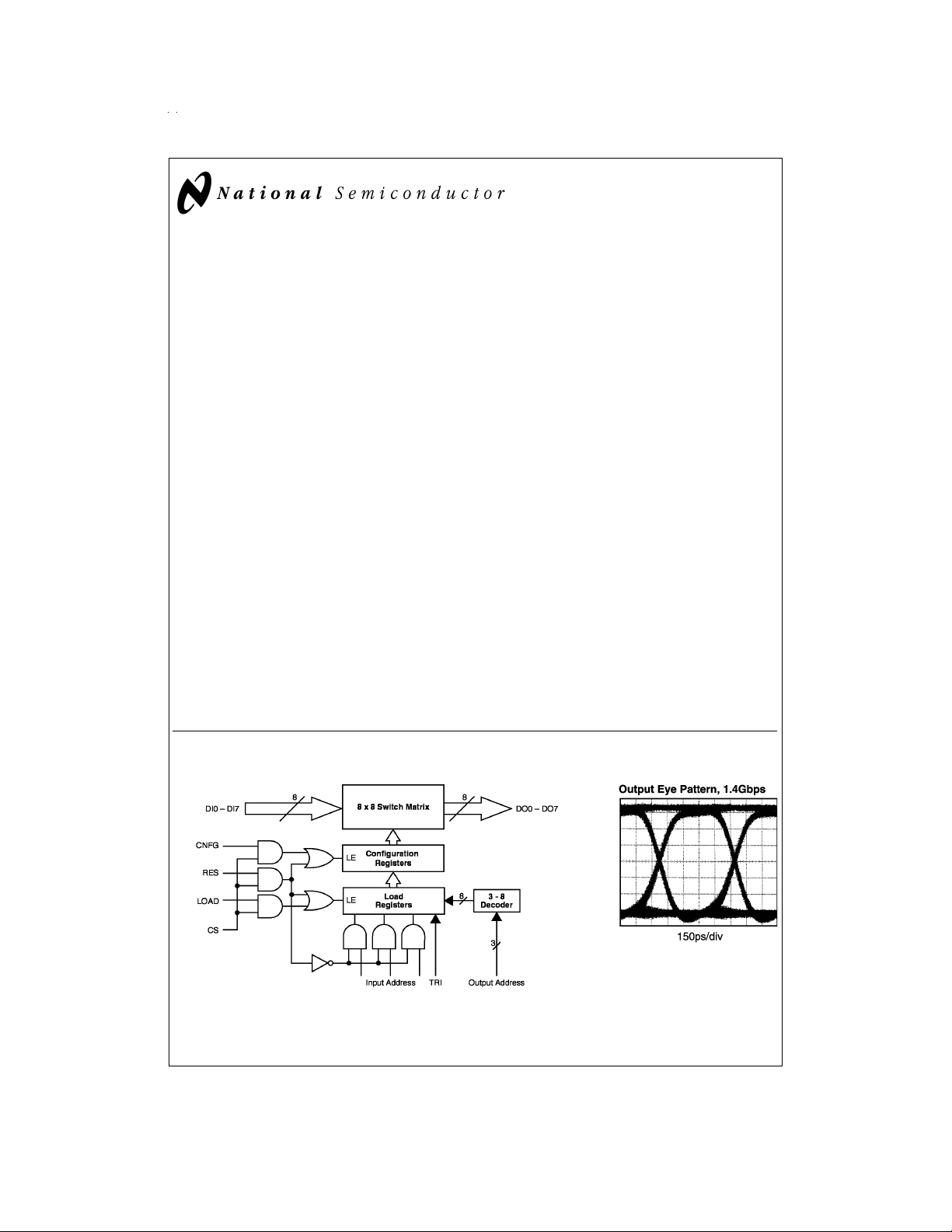
National’s Comlinear CLC018 is a fully differential 8x8 digital
crosspoint switch capable of operating at data rates exceeding 1.4 Gbps per channel. Its non-blocking architecture utilizes eight independent 8:1 multiplexers to allow each output
to be independently connected to any input and any input to
be connected to any or all outputs. Additionally, each output
can be individually disabled and set to a high-impedance
state. This TRI-STATE
larger switch array sizes.
Low channel-to-channel crosstalk allows the CLC018 to provide superior all-hostile jitter of 50ps
fidelity along with low power consumption of 850 mW make
the CLC018 ideal for digital video switching plus a variety of
data communication and telecommunication applications.
The fully differential signal path provides excellent noise immunity, and the I/Os support ECL and PECL logic levels. In
addition, the inputs may be driven single-ended or differentially and accept a wide range of common mode levels including the positive supply. Single +5V or −5V supplies or
dual +5V supplies are supported. Dual supply mode allows
the control signals to be referenced to the positive supply
(+5V) while the high-speed I/O remains ECL compatible.
The double row latch architecture utilized in the CLC018 allows switch reprogramming to occur in the background during operation.Activationofthenew configuration occurs with
a single “configure” pulse. Data integrity and jitter performance on unchanged outputs are maintained during reconfiguration. Two reset modes are provided. Broadcast reset
results in all outputs being connected to input port DI0.
TRI-STATE Reset results in all outputs being disabled.
®
feature allows flexible expansion to
. This excellent signal
PP
The CLC018 is fabricated on a high-performance BiCMOS
process and is available in a 64-lead plastic quad flat pack
(PQFP).
Features
n Fully differential signal path
n Non-Blocking
n Flexible expansion to larger array sizes with very low
power
n Single +5/−5V or dual
n TRI-STATE outputs
n Double row latch architecture
n 64-lead PQFP package
Applications
n Serial digital video routing (SMPTE 259M)
n Telecom/datacom switching
n ATM SONET
Key Specifications
n High speed:>1.4 Gbps
n Low jitter:
<
50 psPPfor rates<500 Mbps
<
100 psPPfor rates<1.4 Gbps
n Low power; 850 mW with all outputs active
n Fast output edge speeds: 250 ps
±
5V operation
CLC0188x8Digital Crosspoint Switch, 1.4 Gbps
October 1998
CLC018 Block Diagram
DS100088-1
DS100088-2
© 1998 National Semiconductor Corporation DS100088 www.national.com
Page 2
Absolute Maximum Ratings (Note 1)
If Military/Aerospace specified devices are required,
please contact the National Semiconductor Sales Office/
Distributors for availability and specifications.
Supply Voltage (V
Maximum VCC+6V
V
LL
Minimum VCC−0.5V
V
LL
CC–VEE)
Storage Temperature Range −65˚C to +150˚C
Lead Temp. (Soldering 4 sec.) +260˚C
ESD Rating TBD
Package Thermal Resistance
64-Pin PQFP 75˚C/W
θ
JA
−0.3V to +6.0V
θ
64-Pin PQFP 15˚C/W
JC
Reliability Information
Transistor Count 3000
MTTF (based on limited life test data) TBD
Recommended Operating
Conditions
Supply Voltage (VCC–VEE) 4.5V to 5.5V
Operating Temperature −40˚C to +85˚C
V
LL
VCCor VCC+5V
Electrical Characteristics
(VCC= 0V, VEE= −5V, VLL= 0V; unless otherwise specified) (Note 4).
Parameter Conditions
Typ
+25˚C
Min/Max
+25˚C
DYNAMIC PERFORMANCE
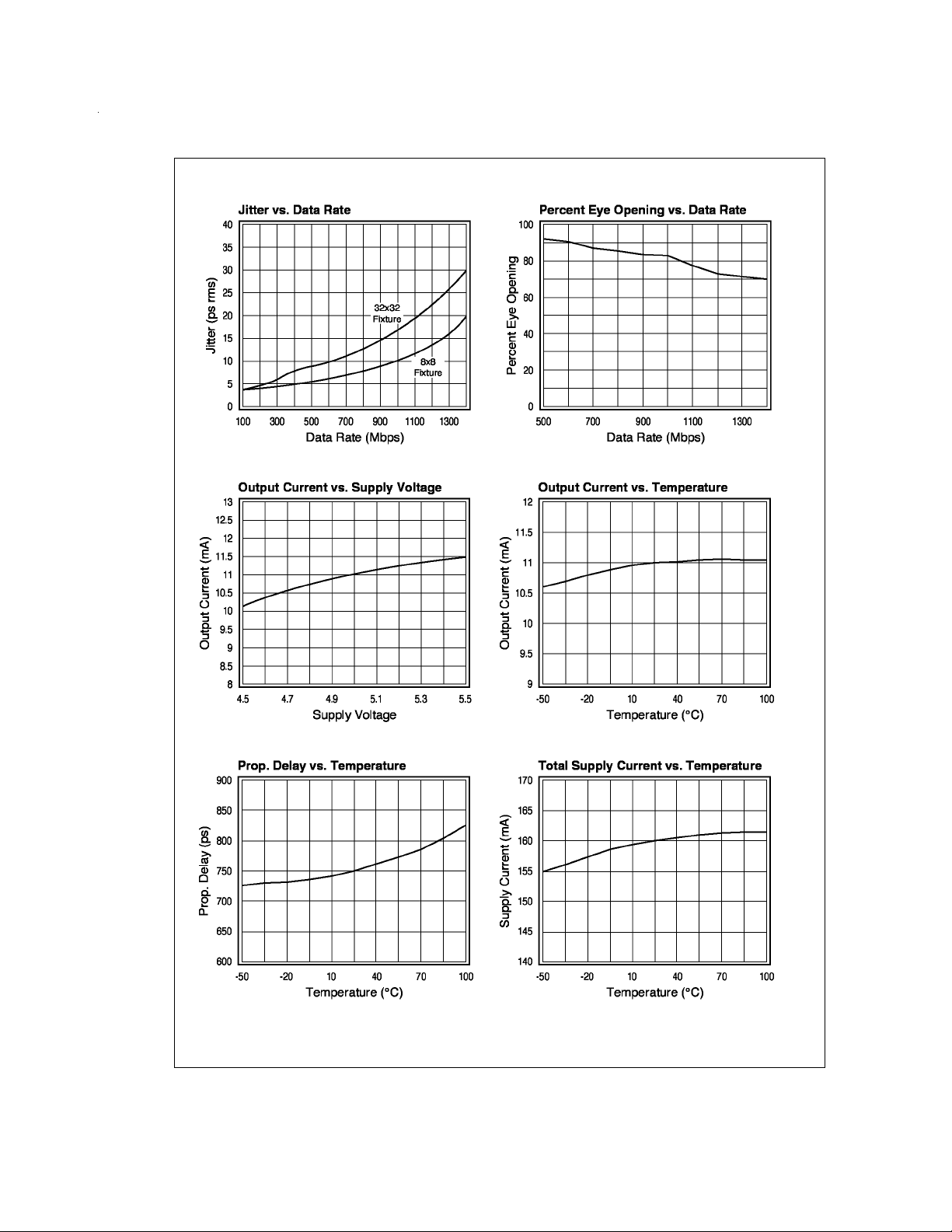
Max. Data Rate/Channel (NRZ) (Note 5) 1.4 Gbps
<
Channel Jitter Data Rate
(Note 6)
Data Rate<1.4 Gbps
(Note 6)
500 Mbps
50 ps
100 ps
Propagation Delay (input to output) 0.75 ns
Propagation Delay Match (Note 7)
±
200 ps
Output Rise/Fall Time (Note 8) 250 ps
Duty Cycle Distortion (Note 9) 10 ps
CONTROL TIMING: CONFIGURATION
OA Bus to LOAD
LOAD
to OA Bus Hold Time (T2)0ns
↓
IA Bus, TRI to LOAD
LOAD
to IA Bus, TRI Hold Time (T4)5ns
↓
Min Pulse Width: (T
Setup Time (T1)15ns
↑
Setup Time (T3)5ns
↓
)
5
LOAD 10 ns
CNFG 10 ns
LOAD
to CNFG↑Delay (T6)0ns
↑
CNFG
to Valid Delay (T7)20ns
↑
CNFG
to Output TRI-STATE Delay (T8)20ns
↑
CNFG
to Output Active Delay (T9)70ns
↑
CONTROL TIMING: RESET (Note 11)
TRI to RES
RES
Min Pulse Width: RES (T
RES
RES
Setup Time (T10)5ns
↑
to TRI Hold Time (T11)5ns
↓
)10ns
to TRI-STATE Mode Delay (T13)20ns
↑
to Broadcast Mode Delay (T14)70ns
↑
12
STATIC PERFORMANCE
Signal I/O:
Min Input Swing, Differential (Note 3) 150 200 200 mV
Input Voltage Range Lower Limit −2 V
Input Voltage Range Upper Limit 0.4 V
Input Bias Current (Notes 3, 12) 1.5 0.4/3.1 0.3/3.8 µA/output
Output Current (Note 3) 10.7 8.53/12.80 7.20/14.3 mA
Min/Max
−40˚C to
+85˚C
Units
PP
PP
PP
www.national.com 2
Page 3
Electrical Characteristics (Continued)
(VCC= 0V, VEE= −5V, VLL= 0V; unless otherwise specified) (Note 4).
Parameter Conditions
Typ
+25˚C
Min/Max
+25˚C
Signal I/O:
Output Voltage Swing R
=75Ω 800 640/960 540/1060 mV
LOAD
Output Voltage Range Lower Limit −2.5 V
Output Voltage Range Upper Limit 0 V
Control Inputs:
Input Voltage - HIGH V
Input Voltage - LOW V
Input Voltage - HIGH V
Input Voltage - LOW V
IH min
IL max
IH min
IL max
Input Current - HIGH V
Input Current - LOW V
(Note 3) −1 −0.5 −0.5 V
(Note 3) −4 −4.5 −4.5 V
VLL= +5V (Note 3) 4 4.5 4.5 V
VLL= +5V (Note 3) 1 0.5 0.5 V
(Note 3) 1 0.2/2.0 0.1/2.5 µA
IH=VLL
−5V (Note 3) −100 −200/10 −250/15 µA
IL=VLL
MISCELLANEOUS PERFORMANCE
V
Supply Current All Outputs Active
CC
Supply Current All Outputs TRI-STATE
V
CC
Supply Current VLL= 0V (Note 3) 2.5 1.7/3.3 1.5/3.5 mA
V
LL
V
Supply Current VLL= +5V (Note 3) 7 mA
LL
(Notes 3, 13, 14)
(Note 3)
157 127/202 119/217 mA
7 3/11 2/12 mA
Input Capacitance 1.5 pF
Output Capacitance 2 pF
Note 1: “Absolute Maximum Ratings” are those values beyond which the safety of the device cannot be guaranteed. They are not meant to imply that the devices
should be operated at these limits. The table of “Electrical Characteristics” specifies conditions of device operation.
Note 2: Min/max ratings are based on product characterization and simulation. Individual parameters are tested as noted. Outgoing quality levels are determined
from tested parameters.
Note 3: J-level spec. is 100%tested at +25˚C.
Note 4: V
Note 5: Bit error rate less than 10
Note 6: Measured using a pseudo-random (2
Note 7: Spread in propagation delays for all input/output combinations.
Note 8: Measured between the 20%and 80%levels of the waveform.
Note 9: Difference in propagation delay for output low-to-high vs. output high-to-low transition.
Note 10: Refer to the
Note 11: Refer to the
Note 12: The bias current for high speed data input depends on the number of data outputs that are selecting that input.
Note 13: The V
Note 14: I
and all VEEsupply pins are bypassed with 0.01 µF ceramic capacitor.
LL
supply current is a function of the number of active data outputs. I
CC
VEE=IVCC+IVLL
−9
over 50%of the bit cell interval.
23
−1 pattern) binary sequence with all other channels active with an uncorrelated signal.
Configuration Timing Diagram
Reset Timing Diagram
.
.
.
18*N+7mAwhere N is an integer from 0 to 8.
VCC
Min/Max
−40˚C to
+85˚C
Units
www.national.com3
Page 4
Typical Performance Characteristics
DS100088-3 DS100088-4
DS100088-5 DS100088-6
DS100088-7 DS100088-8
www.national.com 4
Page 5
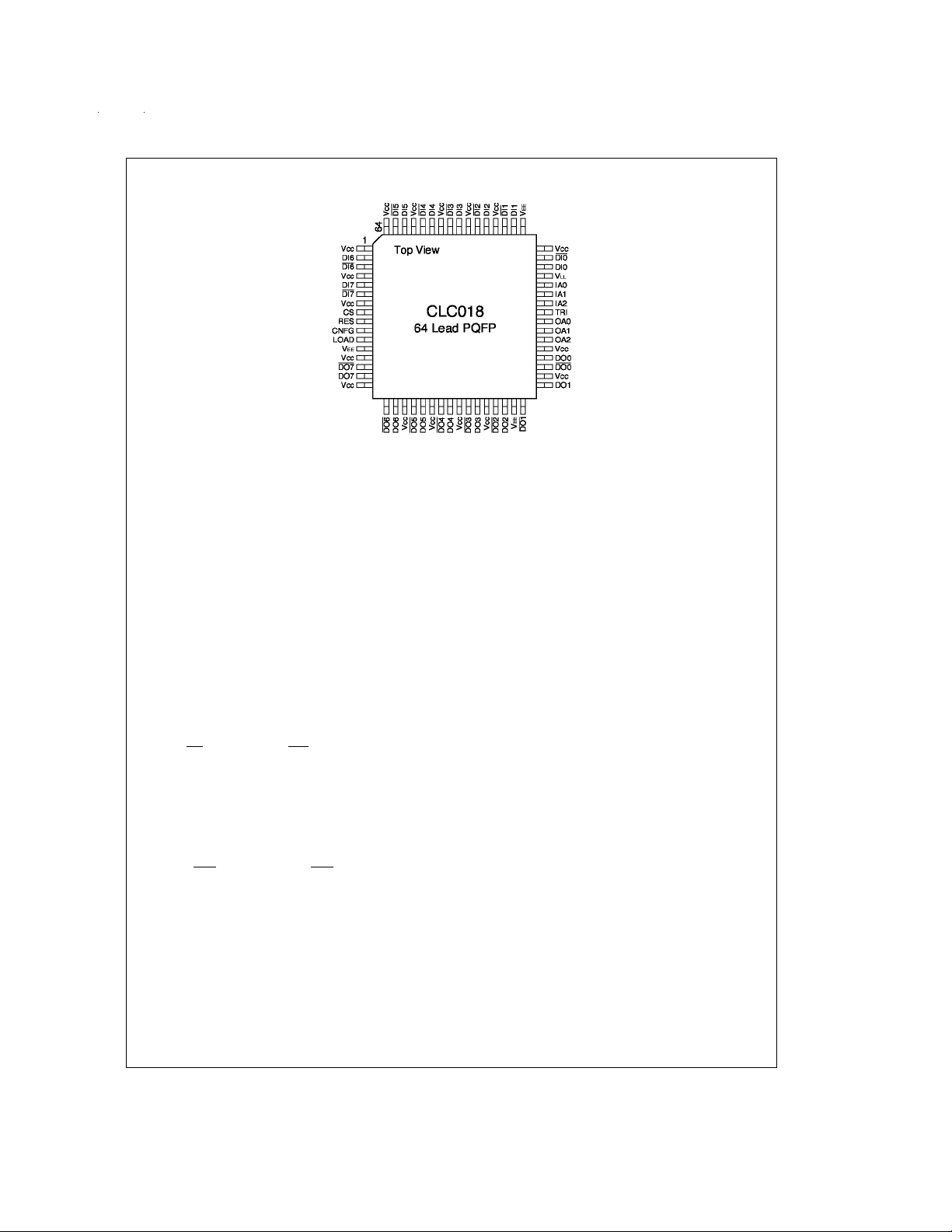
Connection Diagram
Order Number CLC018AJVJQ
See NS Package Number VJE64A
Pin Descriptions
POWER PINS
is the most positive rail for the data path. When the data
V
CC
levels are ECL compatible, then V
GND. For PECL data (+5V referenced ECL), V
nected to the +5V supply. Please refer to the device operation section in this datasheet for recommendations on the
bypassing and ground/power plane requirements of this device.
V
is the most negative rail for the data path. When the data
EE
levels are ECL compatible, then V
power supply. For PECL data (+5V referenced ECL), V
connected to GND.
V
is the logic-level power supply. If the control signals are
LL
referenced to +5V, V
trol signals are ECL compatible, V
is connected to a +5V supply. If con-
LL
DATA INPUT PINS
DI0 and DI0 through DI7 and D17 are the data input pins to
the CLC018. Depending upon how the Power pins are connected (please refer to the Power Pin section above) the
data may be either differential ECL, or differential PECL. To
drive the CLC018 inputs with a single-ended signal, please
refer to the section “Using Single-Ended Data” in the OPERATION section of this datasheet.
DATA OUTPUT PINS
DO0 and DO0 through DO7 and DO7 are the data output
pins of the CLC018. The CLC018 outputs are differential current outputs which can be converted to ECL or PECL compatible outputs through the use of load resistors. Please refer to the “Output Interfacing” paragraph in the OPERATION
section of this datasheet for more details.
should be connected to
CC
is connected to a −5.2V
EE
is connected to GND.
LL
CC
is con-
EE
DS100088-9
CONTROL PINS
IA2, IA1 and IA0 are the three bit input selection address
bus. The input port to be addressed is placed on this bus.
IA2 is the Most Significant Bit (MSB). If input port 6 is to be
addressed, IA2, IA1, IA0 should have 1, 1, 0 asserted on
them. The IA bus should be driven with CMOS levels, if V
is +5V. These levels are thus +5V referenced (standard
CMOS). If V
erenced to the −5V and GND supplies.
is connected to GND, the input levels are ref-
LL
OA2, OA1 and OA0 are the output selection address bus.
The output port selected by the OA bus is connected to the
input port selected on the IAbus when the data is loaded into
the configuration registers. OA2 is the MSB. If OA2, OA1,
is
OA0 are set to 0, 0, 1; then output port 1 will be selected.
CS is an active-high chip select input. When CS is high, the
RES, LOAD, and CNFG pins will be enabled.
LOAD is the latch control for the LOAD register. When LOAD
is high, the load register is transparent. Outputs follow the
state of the IA bus, and are presented to the inputs of the
Configuration register selected by the OA bus. When LOAD
is low, the outputs of the Load register are latched.
RES is the reset control of the configuration and load registers. A high-going pulse on the RES pin programs the switch
matrix to one of two possible states: with TRI low, all outputs
are connected to input #0; with TRI high, all outputs are put
in TRI-STATE condition.
TRI will program the selected output to be in a high impedance or TRI-STATE condition. To place an output in
TRI-STATE, assert a logic-high level on the TRI input when
the desired input and output addresses are asserted on the
respective address inputs and strobe the LOAD input as depicted in the ”Configuration Truth Table”. To enable an output, assert a logic-low level on the TRI input together with the
appropriate addresses and strobe the LOAD input as previously described.
CNFG is the configuration register latch control. When
CNFG is high the Configuration register is made transparent,
and the switch matrix is set to the state loaded into the Load
registers. When CNFG is low, the state of the switch matrix
is latched.
LL
www.national.com5
Page 6
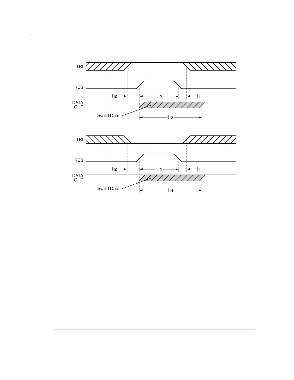
Timing Diagrams
DS100088-10
FIGURE 1. Timing Diagram —TRI-STATE Reset
DS100088-11
FIGURE 2. Timing Diagram —“Broadcast Reset”
www.national.com 6
Page 7

Timing Diagrams (Continued)
FIGURE 3. Timing Diagram —Switch Configuration
Operation
DS100088-12
INPUT INTERFACING
The inputs to the CLC018 are high impedance differential inputs (see the equivalent input circuit in
Figure 4
). The
CLC018 can be operated with either ECL or PECL (+5V referenced ECL), depending upon the power supply connections. The inputs are differential and must both be within the
range of V
–2VtoVCC+ 0.4V in order to function properly.
CC
DS100088-13
FIGURE 4. Equivalent Input Circuit
SINGLE ENDED INPUTS
Differential inputs are the preferred method of providing data
to the CLC018, however, there are times when the only signal available is single ended. To use the CLC018 with a
single ended input, the unused input pin needs to be biased
at a point higher than the low logic level, and lower than the
high logic level. For best noise performance, the middle of
www.national.com7
Page 8

Operation (Continued)
the range is best. For ECL signals this point is about 2 diode
drops below ground. It is possible to bias the unused input
with a low-pass filtered version of the data, as shown in
ure 5
. In some coding schemes there are pathological patterns that result in long sequences with no data transitions.
During these patterns, the bias on the unused input will drift
towards the other input reducing the noise immunity which
makes this scheme undesirable. The most robust solution for
single ended inputs is to place a comparator with hysteresis
in front of the CLC018. Such a part is the MC10E1652. See
Figure 6
for an example of how to hook this up.
FIGURE 5. Single Ended Input to CLC018
FIGURE 6. Single Ended Input to CLC018
OUTPUT INTERFACING
The outputs of the CLC018 are differential, current source
outputs. They can be converted to ECL compatible levels
with the use of resistive loads as shown in
Figure 7
put swings will have a similar temperature coefficient to
10KECLif a 1N4148 diode is used to set V
mercial temperature range applications, a 75Ω resistor can
be used as shown in
Figure 8
. Many circuits with differential
. For most com-
OH
inputs, such as the CLC016 Data Retimer With Automatic
Rate Selection, do not require true ECL levels, so the load
resistors can be connected directly to the positive rail as
shown in
Figure 9
.
DS100088-16
FIGURE 7. Generating 10k ECL Outputs
www.national.com 8
Fig-
DS100088-14
DS100088-15
. The out-
DS100088-17
FIGURE 8. Generating ECL Outputs
DS100088-18
FIGURE 9. Connecting the CLC018 to the CLC016
POWER SUPPLIES, GROUNDING AND BYPASSING
The CLC018 uses separate power supplies for control and
data circuitry. Data circuitry is supplied via V
circuitry via V
supply,is the common return for both. Connection details for
. Supply connection VEE, the negative-most
LL
the different powering modes is shown in
CC
Table 1
and control
.
Internal and external capacitances, normal and parasitic,
must be charged and discharged with changes in output voltage. Charging current depends upon the size of these capacitances and the rate of change of voltage. At the fast transition times of the CLC016, small amounts of stray
capacitance at outputs can produce large output and supply
transient currents. Controlling transient currents requires
particular attention to minimizing stray capacitances and to
providing effective bypassing in the design. Good and effective bypassing consisting of 0.01 µF to 0.1 µF monolithic ceramic and 4.7 µF to 10 µF, 35V tantalum capacitors. These
capacitors should be placed as close to power pins as practical and tightly connected to the power plane sandwich using multiple vias. Needless to say, multilayer board technology should be employed for the CLC018 and similar highfrequency-capability devices.
CONFIGURING THE SWITCH
The CLC018 can be configured so that any output may be independently connected to any input and any input be connected to any or all outputs. Each output may be independently enabled or placed in a high-impedance state.
Data controlling the switch matrix and output mode are
stored in two ranks of eight, 4-bit registers, one register per
output. The three most-significant bits in each register identify the input to be connected to that output. The leastsignificant bit controls whether the output is active or
TRI-STATE. A particular register in the first rank, the LOAD
REGISTERS, is selected by a 3-bit word placed on the out-
Page 9

Operation (Continued)
put address (OA) bus. Data to be written into the load register, consisting of the 3-bit address of the input to be connected to that output and the output-enable control bit, are
placed on the input address (IA) bus. Input data is stored in
the load registers at the low-to-high transition of the LOAD
input pin with chip-select (CS) high-true. The contents of the
load registers are transferred to the second rank of CONFIGURATION REGISTERS at the low-to-high transition of
the CNFG input signal (with CS high). This causes the state
of the entire switch matrix to be set to the selected configuration.
The entire crosspoint may be placed in an initializing state,
with all outputs connected to input-0 and with all outputs either enabled or TRI-STATE. To do so, hold TRI low to make
outputs active, or high to place outputs in TRI-STATE, and
apply a high-going pulse to the RES input pin (with CS high).
In summary, outputs are configured by:
a) first placing the 3-bit address of that output on the OA
bus together with
b) the 3-bit address of the input to be connected to that
output on the IA bus,
c) the output-enable (TRI-STATE) control bit for that output
on the IA bus,
d) making chip-select (CS) true, and then
e) providing a high-going pulse to the LOAD input pin.
f) Repeat these four steps for each output to be config-
ured.
The entire crosspoint matrix may now be configured with the
data held in the load registers. To implement the configuration, apply a high-going pulse to the CNFG input pin. The
contents of the load registers are transferred to the configuration registers and the new configuration of all crosspoints
is effected.
The CLC018 Configuration Truth Table is shown at the end
of the datasheet.
EXPANDING THE SWITCH SIZE
The CLC018 was designed for easy expansion to larger array sizes without paying a significant penalty in either speed
or power. The power dissipation of the expanded array will
be dominated by the number of active outputs, therefore
power will increase linearly with the array size even though
the number of components required increases as the square
of the array size. As an example, a single CLC018 can be
used for an 8x8 array, and it will dissipate about 0.85W.A 32
x 32 array will require 16 CLC018s and will consume only
about 4W.
www.national.com9
Page 10

Operation (Continued)
TABLE 1. Interfacing of the Power Supplies and Bypass Capacitors
Supply Operation Single −5V Single +5V Dual±5V
I/O Data Level ECL PECL ECL
Control Signal Low/High −5V/GND GND/+5V GND/+5V
Connection
Key Information
1. Bypass each V
with a 0.01 µF capacitor.
2. Connect V
the ground plane.
EE
and VLLto
CC
supply
3. A power plane isn’t required for V
be used.
EE
but can
EXPANDING THE NUMBER OF OUTPUT PORTS
To expand the number of output ports in a switch array, the
inputs of multiple CLC018s are connected in parallel. The
bus used to connect the input ports should be a controlled
1. Bypass each V
with a 0.01 µF capacitor.
2. Bypass the V
a 0.01 µF.
3. Connect V
plane.
EE
supply
CC
supply with
LL
to the ground
4. Use a +5V power plane for
V
.
CC
impedance transmission line as shown in
1. Bypass each V
with a 0.01 µF capacitor.
2. Bypass the V
with a 0.01 µF.
3. Connect V
ground plane.
CC
4. A power plane isn’t required for +5V (V
−5V (V
can be used.
) supplies. but
EE
Figure 10
trol the switch array, the IA, OA and TRI busses are all connected in parallel and a decoder is used to assert high the
CS of the CLC018 that is to be addressed. This is also
shown in
Figure 10
.
supply
EE
supply
LL
to the
LL
. To con-
)or
www.national.com 10
Page 11

Operation (Continued)
FIGURE 10.8x16Crosspoint Example
EXPANDING THE NUMBER OF INPUT PORTS
Expanding the number of inputs in a switch array is accomplished by wire-ORing the outputs together, and TRISTATEing the outputs of the CLC018s that do not have their
inputs selected. The output bus should be a controlled impedance transmission line with proper termination. This is
shown in
complemented outputs to control the TRI pins of the
CLC018s in the array. Thus, all CLC018s are programmed
simultaneously, and all of them, except for the one with the
selected input, are placed in the TRI-STATE mode.
Figure 11
. The circuit uses a 1-of-2 decoder with
DS100088-20
EXPANDING BOTH INPUTS AND OUTPUTS
To increase both the number of inputs and outputs in an array,apply both the input port and output port expansion techniques simultaneously. In
case of a 24 input by 32 output switch array. Note that both
input and output busses need to be controlled impedance
transmission lines. The CS pins for rows of CLC018s are
connected together and become the row select inputs,
whereas the TRI pins are connected together for the columns of CLC018s and become the column select pins.
Figure 12
, this is shown for the
www.national.com11
Page 12

Operation (Continued)
FIGURE 11. Expanded Input Ports
www.national.com 12
DS100088-21
Page 13

Operation (Continued)
FIGURE 12. 24 x 32 Output Switch Array
DS100088-22
www.national.com13
Page 14

Operation (Continued)
CALCULATING THE POWER DISSIPATION IN AN
EXPANDED ARRAY
The CLC016 dissipates about 100 mW per active output plus
about 50 mW quiescent power. With all outputs active, this is
about 850 mW. In an expanded array, all devices will dissipate quiescent power, but only those devices with active outputs will dissipate the 100 mW/output. So, an N-by-M device
array (an 8xN-input-by-8xM-output switch) with all outputs
active will dissipateNxMx50mW+8xMx100mW.A32input x 32-output (4 x 4 device) switch array dissipates4x4
x50mW+8x4x100mW=4W.
CONTROLLED IMPEDANCE TRANSMISSION LINES
AND OTHER LAYOUT TECHNIQUES
All transmission lines whose length is greater than
length of the highest frequencies present in the transmitted
signal require proper attention to impedance control to avoid
distortion of the signal. Digital signals are especially susceptible to distortion due to poorly controlled line characteristics
and reflections. With its 250 ps output transitions, which imply a bandwidth of 4 GHz or more, transmission lines driven
by the CLC018 must be carefully designed and correctly terminated. Either microstrip line, which resides on the outer
surfaces of a printed circuit board and paired with an image
ground plane, or stripline, which is sandwiched in an inner
layer between image ground planes, may be used in
CLC018 designs. With either line type, it is important to
maintain a uniform characteristic impedance over the entire
extent of the transmission line system. Likewise, the receiving end of these lines must be terminated in a resistance
equal to the characteristic impedance to preserve signal fidelity.
Figure 13
shows representative methods of interfacing
to and from the CLC018.
Often, when voltage-mode drivers, such as ECL, with low
output impedance (also called equivalent generator resis-
1
⁄4wave-
tance) are used to drive bus networks, a series resistor connects the output of the amplifier to the transmission line. This
resistor serves both as a termination for any signals travelling toward the source- end of the line and as the series leg
of a voltage divider (with the transmission line as the shunt
leg) to reduce the transmitted signal level. This resistor’s correct value is Z
be used successfully in most situations. The receiving end of
. However, a value equal to ZOmay
O−ROUT
the line is terminated in a resistance equal to the value of Z
of the receiving end of the line. A resistance equal to the
line’s Z
works in most situations. In cases where the bus is
O
heavily loaded, the receiving end termination’s value may
need to be reduced to the loaded- Z
the material on distributed loading effects on line characteristics in the
Fairchild F100K ECL 300 Series Databook and
of the line. (Please see
O
Design Guide).
Current-mode drivers, with their high equivalent generator
resistance, when used as bus drivers require a resistance
equal to Z
as appropriate for the design.
at each end of the bus to either power or ground
O
Adetailed discussion of digital transmission line design techniques is beyond the scope of this data sheet, but many
good references are available from National Semiconductor
and others. Extensive material is available in the
terface Databook
tabook and Design Guide
, the
Fairchild F100K ECL 300 Series Da-
and the
Motorola MECL System
National In-
Design Handbook.
Especially useful is the National Semiconductor
sion Line RAPIDESIGNER
905.
The RAPIDESIGNER is available by calling the Na-
r Sliderule and user manual
Transmis-
AN-
tional Semiconductor Customer Response Center in your
area and asking for either Literature Number 633200-001
(ISO Metric units) or 633201-001 (English units). The User
Manual for both versions is Literature Number 100905-002
and is available on our WEB Site at http://www.national.com
as
AN-905.
O
www.national.com 14
Page 15

Operation (Continued)
DS100088-23
FIGURE 13. Input/Output Bussing
www.national.com15
Page 16

Operation (Continued)
Configuration Truth Table
IA2 IA1 IA0 OA2 OA1 OA0 TRI RES LOAD CNFG CS Condition of Device
XXXXXXXX X X 0 NOCHANGE
XXXXXX0
XXXXXX1
XXX00010
XXX00110
XXX01010
XXXCBA 10
•••••••• • • • •
RQPCBA00
•••••••• • • • •
00000000
00000100
00001000
00001100
00010000
00010100
00011000
00011100
00100000
00100100
00101000
00101100
•••••••• • • • •
00111100
•••••••• • • • •
11111000
11111100
XXXXXXX0 0
I
I
X X 1 Load I/P 0 to All O/Ps
X X 1 TRI-STATE All O/P 0
I
I
I
I
I
0 1 TRI-STATE O/P 0
0 1 TRI-STATE O/P 1
0 1 TRI-STATE O/P 2
0 1 TRI-STATE O/P CBA
0 1 Load I/P PQR to O/P
CBA and Enable O/P
CBA
I
I
I
I
I
I
I
I
I
I
I
I
I
I
I
0 1 Load I/P 0 to O/P 0
0 1 Load I/P 0 to O/P 1
0 1 Load I/P 0 to O/P 2
0 1 Load I/P 0 to O/P 3
0 1 Load I/P 0 to O/P 4
0 1 Load I/P 0 to O/P 5
0 1 Load I/P 0 to O/P 6
0 1 Load I/P 0 to O/P 7
0 1 Load I/P 1 to O/P 0
0 1 Load I/P 1 to O/P 1
0 1 Load I/P 1 to O/P 2
0 1 Load I/P 1 to O/P 3
0 1 Load I/P 1 to O/P 7
0 1 Load I/P 7 to O/P 6
0 1 Load I/P 7 to O/P 7
I
1 Activate New
Configuration
www.national.com 16
Page 17

17
Page 18

Physical Dimensions inches (millimeters) unless otherwise noted
CLC0188x8Digital Crosspoint Switch, 1.4 Gbps
64-Lead PQFP
Order Number CLC018AJVJQ
NS Package Number VJE64A
LIFE SUPPORT POLICY
NATIONAL’S PRODUCTS ARE NOT AUTHORIZED FOR USE AS CRITICAL COMPONENTS IN LIFE SUPPORT DEVICES OR SYSTEMS WITHOUT THE EXPRESS WRITTEN APPROVAL OF THE PRESIDENT OF NATIONAL SEMICONDUCTOR CORPORATION. As used herein:
1. Life support devices or systems are devices or systems which, (a) are intended for surgical implant into
the body, or (b) support or sustain life, and whose failure to perform when properly used in accordance
2. A critical component in any component of a life support
device or system whose failure to perform can be reasonably expected to cause the failure of the life support
device or system, or to affect its safety or effectiveness.
with instructions for use provided in the labeling, can
be reasonably expected to result in a significant injury
to the user.
National Semiconductor
Corporation
Americas
Tel: 1-800-272-9959
Fax: 1-800-737-7018
Email: support@nsc.com
www.national.com
National Semiconductor
Europe
Fax: +49 (0) 1 80-530 85 86
Email: europe.support@nsc.com
Deutsch Tel: +49 (0) 1 80-530 85 85
English Tel: +49 (0) 1 80-532 78 32
Français Tel: +49 (0) 1 80-532 93 58
Italiano Tel: +49 (0) 1 80-534 16 80
National Semiconductor
Asia Pacific Customer
Response Group
Tel: 65-2544466
Fax: 65-2504466
Email: sea.support@nsc.com
National Semiconductor
Japan Ltd.
Tel: 81-3-5620-6175
Fax: 81-3-5620-6179
National does not assume any responsibility for use of any circuitry described, no circuit patent licenses are implied and National reserves the right at any time without notice to change said circuitry and specifications.
 Loading...